EP2040365A2 - Convertisseur progressif avec des redresseurs synchrones à entraînement automatique - Google Patents
Convertisseur progressif avec des redresseurs synchrones à entraînement automatique Download PDFInfo
- Publication number
- EP2040365A2 EP2040365A2 EP08162527A EP08162527A EP2040365A2 EP 2040365 A2 EP2040365 A2 EP 2040365A2 EP 08162527 A EP08162527 A EP 08162527A EP 08162527 A EP08162527 A EP 08162527A EP 2040365 A2 EP2040365 A2 EP 2040365A2
- Authority
- EP
- European Patent Office
- Prior art keywords
- terminal
- slave
- rectifier
- resistor
- bipolar transistor
- Prior art date
- Legal status (The legal status is an assumption and is not a legal conclusion. Google has not performed a legal analysis and makes no representation as to the accuracy of the status listed.)
- Granted
Links
Images







Classifications
-
- H—ELECTRICITY
- H02—GENERATION; CONVERSION OR DISTRIBUTION OF ELECTRIC POWER
- H02M—APPARATUS FOR CONVERSION BETWEEN AC AND AC, BETWEEN AC AND DC, OR BETWEEN DC AND DC, AND FOR USE WITH MAINS OR SIMILAR POWER SUPPLY SYSTEMS; CONVERSION OF DC OR AC INPUT POWER INTO SURGE OUTPUT POWER; CONTROL OR REGULATION THEREOF
- H02M3/00—Conversion of DC power input into DC power output
- H02M3/22—Conversion of DC power input into DC power output with intermediate conversion into AC
- H02M3/24—Conversion of DC power input into DC power output with intermediate conversion into AC by static converters
- H02M3/28—Conversion of DC power input into DC power output with intermediate conversion into AC by static converters using discharge tubes with control electrode or semiconductor devices with control electrode to produce the intermediate AC
- H02M3/325—Conversion of DC power input into DC power output with intermediate conversion into AC by static converters using discharge tubes with control electrode or semiconductor devices with control electrode to produce the intermediate AC using devices of a triode or a transistor type requiring continuous application of a control signal
- H02M3/335—Conversion of DC power input into DC power output with intermediate conversion into AC by static converters using discharge tubes with control electrode or semiconductor devices with control electrode to produce the intermediate AC using devices of a triode or a transistor type requiring continuous application of a control signal using semiconductor devices only
- H02M3/33569—Conversion of DC power input into DC power output with intermediate conversion into AC by static converters using discharge tubes with control electrode or semiconductor devices with control electrode to produce the intermediate AC using devices of a triode or a transistor type requiring continuous application of a control signal using semiconductor devices only having several active switching elements
- H02M3/33576—Conversion of DC power input into DC power output with intermediate conversion into AC by static converters using discharge tubes with control electrode or semiconductor devices with control electrode to produce the intermediate AC using devices of a triode or a transistor type requiring continuous application of a control signal using semiconductor devices only having several active switching elements having at least one active switching element at the secondary side of an isolation transformer
- H02M3/33592—Conversion of DC power input into DC power output with intermediate conversion into AC by static converters using discharge tubes with control electrode or semiconductor devices with control electrode to produce the intermediate AC using devices of a triode or a transistor type requiring continuous application of a control signal using semiconductor devices only having several active switching elements having at least one active switching element at the secondary side of an isolation transformer having a synchronous rectifier circuit or a synchronous freewheeling circuit at the secondary side of an isolation transformer
-
- H—ELECTRICITY
- H02—GENERATION; CONVERSION OR DISTRIBUTION OF ELECTRIC POWER
- H02M—APPARATUS FOR CONVERSION BETWEEN AC AND AC, BETWEEN AC AND DC, OR BETWEEN DC AND DC, AND FOR USE WITH MAINS OR SIMILAR POWER SUPPLY SYSTEMS; CONVERSION OF DC OR AC INPUT POWER INTO SURGE OUTPUT POWER; CONTROL OR REGULATION THEREOF
- H02M3/00—Conversion of DC power input into DC power output
- H02M3/22—Conversion of DC power input into DC power output with intermediate conversion into AC
- H02M3/24—Conversion of DC power input into DC power output with intermediate conversion into AC by static converters
- H02M3/28—Conversion of DC power input into DC power output with intermediate conversion into AC by static converters using discharge tubes with control electrode or semiconductor devices with control electrode to produce the intermediate AC
- H02M3/325—Conversion of DC power input into DC power output with intermediate conversion into AC by static converters using discharge tubes with control electrode or semiconductor devices with control electrode to produce the intermediate AC using devices of a triode or a transistor type requiring continuous application of a control signal
- H02M3/335—Conversion of DC power input into DC power output with intermediate conversion into AC by static converters using discharge tubes with control electrode or semiconductor devices with control electrode to produce the intermediate AC using devices of a triode or a transistor type requiring continuous application of a control signal using semiconductor devices only
- H02M3/33561—Conversion of DC power input into DC power output with intermediate conversion into AC by static converters using discharge tubes with control electrode or semiconductor devices with control electrode to produce the intermediate AC using devices of a triode or a transistor type requiring continuous application of a control signal using semiconductor devices only having more than one ouput with independent control
-
- Y—GENERAL TAGGING OF NEW TECHNOLOGICAL DEVELOPMENTS; GENERAL TAGGING OF CROSS-SECTIONAL TECHNOLOGIES SPANNING OVER SEVERAL SECTIONS OF THE IPC; TECHNICAL SUBJECTS COVERED BY FORMER USPC CROSS-REFERENCE ART COLLECTIONS [XRACs] AND DIGESTS
- Y02—TECHNOLOGIES OR APPLICATIONS FOR MITIGATION OR ADAPTATION AGAINST CLIMATE CHANGE
- Y02B—CLIMATE CHANGE MITIGATION TECHNOLOGIES RELATED TO BUILDINGS, e.g. HOUSING, HOUSE APPLIANCES OR RELATED END-USER APPLICATIONS
- Y02B70/00—Technologies for an efficient end-user side electric power management and consumption
- Y02B70/10—Technologies improving the efficiency by using switched-mode power supplies [SMPS], i.e. efficient power electronics conversion e.g. power factor correction or reduction of losses in power supplies or efficient standby modes
Definitions
- the present invention relates to a forward converter with self-driven synchronous rectifiers.
- a forward converter can be used to convert a high DC voltage source into multiple low DC voltage sources, where the master output is regulated by a closed-loop pulse width modulation (PWM) controller and slave outputs are regulated by secondary side post regulators (SSPR).
- PWM pulse width modulation
- SSPR secondary side post regulators
- FIG. 1 is a block diagram illustrating the master output with synchronous rectifiers.
- the secondary power loop comprises a secondary power winding T s , a forward synchronous rectifier M f , a freewheeling synchronous rectifier M w , a power inductor L 1 and a filter capacitor C 1 .
- the closed-loop PWM controller comprises three blocks: (1) an error-amplifier circuit 1 samples the output voltage V 1 through a voltage divider and compares the output voltage sample with a reference voltage to generate an amplified error signal (voltage or current); (2) a control circuit 2 converts the amplified error signal into a PWM signal and (3) a drive circuit 3 converts the PWM signal into drive signals of M f and M w .
- the block diagrams of slave outputs with diode rectifiers are shown in FIG.2a and FIG.2b .
- the secondary power loop comprises a secondary power winding T s2 , a secondary side post regulator (SSPR) S 1 , a forward diode rectifier D f , a freewheeling diode rectifier D w , a power inductor L 2 and a filter capacitor C 2 .
- S 1 can be placed at either the high-side ( FIG. 2a ) or the low-side ( FIG. 2b ).
- D f can be placed at either the high-side or the low-side, depending on the materialization of S 1 .
- S 1 can be implemented with either a magnetic amplifier (MA) or a controlled switch (CS).
- MA magnetic amplifier
- CS controlled switch
- S 1 is implemented with a MA, D f must be placed at the high-side and the switch controller 4 is a reset circuit. If S 1 is implemented with a CS, D f can be placed at either the high-side or the low-side and the switch controller 4 is a drive circuit. S 1 blanks the leading edge of the voltage waveform across T s2 so that the average value of the voltage waveform across D w equals the output voltage V 2 .
- the blanking effect of S 1 is illustrated with FIG. 3 , where V L1 is the voltage across L 1 in FIG. 1 and V L2 is the voltage across L 2 in either FIG. 2a or FIG. 2b .
- the voltage across T s is positive with respect to its reference polarity; M f is turned on but M w is turned off; V L1 is positive with respect to its reference polarity; L 1 stores electric energy through T s , M f and C 1 .
- the voltage across T s2 is positive with respect to its reference polarity; S 1 is turned off; the voltage waveform across T s2 is blanked by S 1 ; no current flows through D f ; the continuous current of L 2 forces D w to conduct; V L2 is negative with respect to its reference polarity; L 2 releases electric energy through D w and C 2 .
- the voltage across T s2 is positive with respect to its reference polarity; S 1 is turned on; the voltage waveform across T s2 is not blanked by S 1 ; the continuous current of L 2 commutates from D w to D f ; V L2 is positive with respect to its reference polarity; L 2 stores electric energy through D f , T s2 , S 1 and C 2 .
- the voltage across T s is negative with respect to its reference polarity; M f is turned off but M w is turned on; V L1 is negative with respect to its reference polarity; L 1 releases electric energy through M w and C 1 ; the voltage across T s2 is negative with respect to its reference polarity; S 1 is turned off; the continuous current of L 2 commutates D f from to D w ; V L2 is negative with respect to its reference polarity; L 2 releases electric energy through D w and C 2 .
- the voltage across T s is 0; M f is turned off but M w is still turned on; V L1 is negative with respect to its reference polarity; L 1 releases electric energy through M w and C 1 ; the voltage across T s2 is 0; S 1 is turned off; D f is turned off but D w is turned on; V L2 is negative with respect to its reference polarity; L 2 releases electric energy through D w and C 2 .
- M f and M w are referred to as IC-driven synchronous rectifiers. If it is based on a secondary driving winding, M f and M w are referred to as self-driven synchronous rectifiers.
- a drive circuit based on an IC is more complicated and expensive than a drive circuit based on a secondary driving winding.
- D f and D w in either FIG. 2a or FIG.2b suffer from higher rectifier conduction loss. Therefore, the present invention discloses a cost-effective approach to drive the self-driven synchronous rectifiers in the master output and slave outputs simultaneously.
- the present invention is directed to a multiple-output forward converter with self-driven synchronous rectifiers.
- the drive circuit comprises a secondary driving winding, a level shifter (optional) and a signal distributor.
- the secondary driving winding induces a bipolar driving voltage from the forward transformer.
- the level shifter shifts the bipolar driving voltage by a predetermined level to a shifted bipolar driving voltage.
- the signal distributor distributes the (shifted) bipolar driving voltage to the gates of the forward and freewheeling synchronous rectifiers.
- the forward synchronous rectifier can be placed at either the high-side or the low-side. If the forward synchronous rectifier is placed at the high-side, it is self-driven by an additional secondary driving winding. If the forward synchronous rectifier is placed at the low-side, it can be self-driven by either an additional secondary driving winding or the driving voltage of the master forward synchronous rectifier.
- the freewheeling synchronous rectifier is self-driven by the driving voltage of the master freewheeling synchronous rectifier.
- FIG. 4 is a block diagram illustrating a schematic circuit of the master output of a multiple-output forward converter according to the present invention.
- the forward transformer includes a primary power winding T 1 , a secondary power winding T 2 and a secondary driving winding T 3 .
- the two terminals of the primary winding T 1 are connected in series to an input voltage V i through one or two primary switches (not shown).
- the secondary power winding T 2 connecting a master power loop 21, includes a voltage output terminal (high voltage terminal) and a ground terminal (low voltage terminal) to provide a voltage V i for driving an external load circuit (not shown).
- a filter capacitor C 3 is connected between the voltage output terminal and the ground terminal.
- a power inductor L 3 is connected between the first terminal (marked with a dot) of the secondary power winding T 2 and the voltage output terminal.
- the dots of the primary and the secondary windings mean the same electric polarity.
- the master power loop 21 includes a forward synchronous rectifier 211, a freewheeling synchronous rectifier 212 and a power inductor L 3 .
- Each of the two synchronous rectifiers 211 and 212 includes a first terminal, a second terminal and a control terminal, where the control terminal receives a voltage signal to control the turn-on or turn-off of the channel between the first terminal and the second terminal.
- the first terminals of the two synchronous rectifiers 211 and 212 are respectively connected to the two terminals of the secondary power winding T 2 ; both of the second terminals of the two synchronous rectifiers 211 and 212 are connected to the common ground terminal Z M .
- a signal distributor 22 comprises a first output terminal, a second output terminal and a common connection terminal.
- the first output terminal and the second output terminal are respectively connected to the two terminals of the secondary driving winding T 3 as well as the control terminals of the two synchronous rectifiers 211 and 212.
- the common connection terminal is connected to the common ground terminal Z M .
- the first output terminal of the signal distributor 22 When the voltage across T 3 is positive with respect to its reference polarity, the first output terminal of the signal distributor 22 is connected with the common connection terminal; a positive voltage signal is distributed to the control terminal of the forward synchronous rectifier 211; the channel of the forward synchronous rectifier 211 is turned on.
- the second output terminal of the signal distributor 22 When the voltage across T 3 is negative with respect to its reference polarity, the second output terminal of the signal distributor 22 is connected with the common connection terminal; a positive voltage signal is distributed to the control terminal of the freewheeling synchronous rectifier 212; the channel of the freewheeling synchronous rectifier 212 is turned on.
- FIG. 5 illustrates a practical circuit of the master output according to the embodiment in FIG. 4 .
- two nMOSFET transistors M 1 and M 2 are respectively used as the forward synchronous rectifier 211 and the freewheeling synchronous rectifier 212 and referred to as a forward transistor M 1 and a freewheeling transistor M 2 respectively.
- gates, drains and sources of M 1 and M 2 respectively serve as the control terminals, the first terminals and the second terminals.
- the signal distributor 22 includes two diodes D 1 and D 2 .
- the anodes of D 1 and D 2 are connected to each other and the common ground terminal Z M .
- the cathodes of D 1 and D 2 respectively serve as the first output terminal and the second output terminal and are connected to the gates of M 2 and M 1 .
- FIG. 6 illustrates voltage waveforms of the secondary drive winding, the gate of the forward synchronous rectifier and the gate of the freewheeling synchronous rectifier within one switching period in the master output according to the embodiment in FIG. 5 .
- the voltage across T 3 is V s ; D 1 is turned on by a forward bias but D 2 is turned off by a reverse bias; the signal distributor 22 distributes a positive voltage V s and a zero voltage 0 to the gates of M 1 and M 2 , respectively; L 3 stores electric energy through T 2 , M 1 and C 3 .
- the voltage across T 3 is -V s ; D 2 is turned on by a forward bias but D 1 is turned off by a reverse bias; the signal distributor 22 distributes a positive voltage V s and a zero voltage 0 to the gates of M 2 and M 1 ,respectively; L 3 releases electric energy through M 2 and C 3 .
- the level shifter 23 includes a first input terminal, a second input terminal, a first output terminal and a second output terminal.
- the first input terminal and the second input terminal of the level shifter 23 are respectively connected to both terminals of T 3 .
- the first output terminal and the second output terminal of the level shifter 23 are respectively connected to the first output terminal and the second output terminal of the signal distributor 22.
- the second output terminal is identical to the second input terminal.
- FIG. 8 illustrates a preferred circuit of the master output according to the embodiment in FIG. 7 .
- the level shifter 23 comprises a second capacitor C 4 , a diode D 4 and a Zener diode ZD 4 .
- One terminal of C 4 serves as the first input terminal and the other terminal of C 4 serves as the first output terminal, which is also connected with the anode of D 4 .
- the anode of ZD 4 serves as the second input terminal as well as the second output terminal.
- the cathode of D 4 is connected with the cathode of ZD 4 .
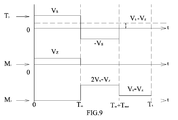
- FIG. 9 illustrates voltage waveforms of the secondary drive winding, the gate of the forward synchronous rectifier and the gate of the freewheeling synchronous rectifier within one switching period in the master output according to the embodiment in FIG. 8 .
- the dashed line marks the output voltage waveform of the level shifter.
- the voltage across T 3 is V s ; D 4 is turned on by a forward bias; ZD 4 breaks down; C 4 is recharged to a voltage V r ; D 1 is turned on by a forward bias but D 2 is turned off by a reverse bias; the signal distributor 22 distributes a positive voltage V z and a zero voltage to the gates of M 1 and M 2 , respectively; L 3 stores electric energy through T 2 , M 1 and C 3 .
- the voltage across T 3 is -V s ; both D 4 and ZD 4 are turned off; D 2 is turned on by a forward bias but D 1 is turned off by a reverse bias; the signal distributor 22 distributes a positive voltage 2V s -V z and a zero voltage to the gates of M 2 and M 1 , respectively; L 3 releases electric energy through M 2 and C 3 .
- the voltage across T 3 is 0; both D 4 and ZD 4 are turned off; D 2 is turned on by a forward bias but D 1 is turned off by a reverse bias; the signal distributor 22 distributes a positive voltage V s -V z and a zero voltage to the gates of M 2 and M 1 , respectively; L 3 releases electric energy through M 2 and C 3 .
- Table 1 lists the comparison between FIG. 6 and FIG. 9 : Table 1 on-interval reset-interval dead-interval without level shifter with level shifter without level shifter with level shifter without level shifter with level shifter M 1 V s V z 0 0 0 0 M 2 0 0 V s 2V s -V z 0 V s -V z
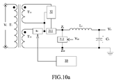
- FIG. 10a and FIG. 10b illustrate two alternative schematic circuits of slave outputs of multiple-output forward converter with self-driven synchronous rectifiers according to an embodiment of the present invention, wherein the SSPRs S 2 can be placed at high-side or low-side, and the SSPR S 2 can be implemented with either a magnetic amplifier (MA) driven by a reset circuit or a controlled switch (CS) driven by an integrated circuit (IC) driver.
- MA magnetic amplifier
- CS controlled switch
- IC integrated circuit
- S 2 is implemented with a MA
- the forward synchronous rectifier 311 is emphatically placed at the high-side and self-driven by an additional drive circuit 32 based on an additional secondary driving winding T 13 , and the switch controller 33 is a reset circuit.
- the forward synchronous rectifier 311 can be placed at the low-side or high-side and self-driven by the additional drive circuit 32, and the switch controller 33 is an IC driver. Moreover, the slave forward synchronous rectifier 311 can be driven by the driving voltage of the master forward synchronous rectifier shown as FIG. 16 .
- the slave power loop includes a forward rectifier 311, a freewheeling rectifier 312, a power inductor L 5 , a SSPR S 2 and a slave filter capacitor C 5 .
- the slave forward rectifier 311, the slave freewheeling rectifier 312 and the power inductor L 5 are connected at the common point Z s .
- the other terminal of the power inductor L 5 connected to an auxiliary voltage output terminal.
- the slave filter capacitor C 5 is connected between the auxiliary voltage output terminal and the ground terminal of the slave power loop for providing a slave output voltage V 2 .
- the slave forward rectifier 311 and the slave freewheeling rectifier 312 is connected at the common ground terminal, same as the common ground terminal Z m of the master power loop.
- an additional secondary driving winding T 13 is used to drive the additional drive circuit 32.
- FIG. 11a , FIG. 12a and FIG. 13a are three alternative circuit diagrams of slave outputs according to the example of high-side SSPR S 2 shown in FIG. 10a
- FIG. 11b , FIG. 12b and FIG. 13b are three alternative circuit diagrams of slave outputs according to the example of low-side SSPR S 2 shown FIG 10b
- the slave forward rectifier 311 and the slave freewheeling rectifier is implemented, but not limited, by nMOSFET transistors, noted a synchronous forward transistor M 7 and a synchronous freewheeling transistor M 8 .
- the drains, sources and gates of the forward transistor M 7 and the freewheeling transistor M 8 serve as the first terminals, second terminals and the control terminals of the slave forward rectifiers 311 and the freewheeling rectifiers 312 respectively, and the drains are connected at the common point Z s .
- the examples respectively shown in FIG.11a , FIG. 11b , FIG.12a and FIG. 12b are unipolar driving mode, which means the driving voltage is always the same (direct).
- the examples respectively shown in FIG. 13a and FIG. 13b are bipolar driving mode, which means the driving voltage is alternative.
- the drive circuit 32 includes a diode D 7 and an interlocked switch circuit.
- the interlocked switch circuit includes an NPN bipolar transistor Q 1 , a PNP bipolar transistor Q 2 , and two resistors R 1 and R 2 . Emitters of the transistors Q 1 and Q 2 are connected at a connection point, and the connection point is connected to the gate of the forward transistor M 7 . Bases of the two transistors Q 1 and Q 2 are connected at another point and the point is connected to the collectors of the transistors Q 1 and Q 2 through the resistors R 1 and R 2 , respectively.
- the collectors of the transistors Q 1 and Q 2 are connected to a cathode of the diode D 7 and the second terminal of the secondary driving winding T 13 respectively, and then the anode of the diode D 7 is connected to the first terminal of the secondary driving winding T 13 .
- the drive circuit 32 includes two resistors R 3 , R 4 and an interlocked switch circuit.
- the interlocked switch circuit includes a diode D s and a PNP bipolar transistor Q 3 , wherein the anode and the cathode of the diode D s are connected to the base and emitter of Q 3 .
- the base of Q 3 is connected to the dotted terminal (first terminal) of the slave secondary driving winding T 13 .
- the collector and the emitter of Q 3 are connected to the second terminal of the slave secondary driving winding T 13 and the gate of the slave forward transistor M 7 .
- the resistor R 4 is connected between the collector and the emitter of the Q 3 .
- Table 2 lists the polarities of the voltage across T 13 and the gate voltage of M 7 within one switching period according to the embodiments in FIG. 11a , FIG.11b , FIG.12a and FIG. 12b : Table 2 on-interval reset-interval dead-interval T 13 M 7 T 13 M 7 T 13 M 7 + + - 0 0 0
- the drive circuit 32 merely includes two resistors R 1 and R 2 connected with each other, which are respectively connected to the first terminal and the second terminal of the secondary driving winding T 13 .
- the connection point of the resistors R 1 and R 2 is connected to the gate of the forward transistor M 7 , and the resistor R 2 is connected between the gate and the source of the forward transistor M 7 .
- Table 3 lists the polarities of the voltage across T 13 and the gate voltage of M 7 within one switching period according to the embodiments in FIG. 13a and FIG. 13b : Table 3 on-interval reset-interval dead-interval T 13 M 7 T 13 M 7 T 13 M 7 + + - - 0 0
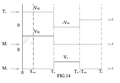
- FIG. 14 illustrates the time sequence of the voltage waveforms of the secondary drive winding T 13 , the gate of the synchronous forward transistor M 7 and the gate of the synchronous freewheeling transistor M 8 of the slave outputs of the examples shown in FIG. 11a , FIG. 11b , FIG. 12a and FIG. 12b accompanying with the master output of the example shown in FIG. 5 within one switching period.
- the voltage across T 13 is V s2 ; M 7 is turned on by a positive driving voltage V s2 but M 8 is turned off by a zero driving voltage.
- the voltage across T 14 is positive with respect to its reference polarity; S 2 is turned off; the voltage waveform across T 14 is blanked by S 2 ; no current flows through the channel or body diode of M 7 ; the continuous current of L 5 forces the body diode of M 8 to conduct; L 5 releases electric energy through the body diode of M 8 and C 5 .
- FIG. 15 illustrates the time sequence of the voltage waveforms of the secondary drive winding T 13 , the gate of the synchronous forward transistor M 7 and the gate of the synchronous freewheeling transistor M 8 of the slave outputs of the examples shown in FIG. 11a , FIG. 11b , FIG. 12a and FIG. 12b accompanying with the master output of the example shown in FIG. 8 within one switching period.
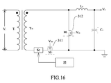
- FIG. 16 illustrates a circuit of slave outputs with a low-side SSPR S 2 and a low-side slave synchronous forward transistor M7 , and the SSPR S 2 is a controlled switch. As shown, the example does not need a slave drive circuit.
- the slave synchronous forward transistor M 7 and the slave synchronous freewheeling transistor M 8 are driven by the driving voltages of the master synchronous forward transistor and the master synchronous freewheeling transistor.
- FIG. 17a and FIG. 17b illustrate the time sequence of the voltage waveforms of the gate of the slave synchronous forward transistor M 7 and the gate of the slave synchronous freewheeling transistor M 8 of the example shown in FIG. 16 accompanying with the master output shown in FIG.5 and FIG. 8 respectively within one switching period.
- M 7 is turned on by positive driving voltages V s ( FIG. 17a ) and V z ( FIG. 17b ) but M 8 is turned off by a zero driving voltage.
- M 7 is turned off by a zero driving voltage but M 8 is turned on by positive driving voltages V s ( FIG.
- the forward transistor and the freewheeling transistor may be but not limited to an N-channel metal-oxide semiconductor field-effect transistor (N-channel MOSFET), a P metal-oxide semiconductor field-effect transistor (P-channel MOSFET), an N-channel junction field effect transistor (N-channel JFET) or a P-channel junction field effect transistor (P-channel JFET).
- N-channel MOSFET N-channel metal-oxide semiconductor field-effect transistor
- P-channel MOSFET P metal-oxide semiconductor field-effect transistor
- N-channel JFET N-channel junction field effect transistor
- P-channel JFET P-channel junction field effect transistor
Landscapes
- Engineering & Computer Science (AREA)
- Power Engineering (AREA)
- Dc-Dc Converters (AREA)
- Rectifiers (AREA)
Applications Claiming Priority (1)
| Application Number | Priority Date | Filing Date | Title |
|---|---|---|---|
| TW096135431A TWI363477B (en) | 2007-09-21 | 2007-09-21 | Forward converter with self-driven synchronous rectifier |
Publications (3)
| Publication Number | Publication Date |
|---|---|
| EP2040365A2 true EP2040365A2 (fr) | 2009-03-25 |
| EP2040365A3 EP2040365A3 (fr) | 2009-11-25 |
| EP2040365B1 EP2040365B1 (fr) | 2011-12-28 |
Family
ID=40219433
Family Applications (1)
| Application Number | Title | Priority Date | Filing Date |
|---|---|---|---|
| EP08162527A Not-in-force EP2040365B1 (fr) | 2007-09-21 | 2008-08-18 | Convertisseur progressif avec des redresseurs synchrones à entraînement automatique |
Country Status (5)
| Country | Link |
|---|---|
| US (1) | US7885086B2 (fr) |
| EP (1) | EP2040365B1 (fr) |
| JP (1) | JP2009077623A (fr) |
| AT (1) | ATE539480T1 (fr) |
| TW (1) | TWI363477B (fr) |
Cited By (1)
| Publication number | Priority date | Publication date | Assignee | Title |
|---|---|---|---|---|
| CN112448600A (zh) * | 2019-09-03 | 2021-03-05 | 西安航兴海拓电子科技有限公司 | 一种综合电源 |
Families Citing this family (9)
| Publication number | Priority date | Publication date | Assignee | Title |
|---|---|---|---|---|
| TWI429195B (zh) * | 2010-12-08 | 2014-03-01 | Ind Tech Res Inst | 功率電路及其直流對直流轉換器 |
| US8908393B2 (en) * | 2011-09-14 | 2014-12-09 | Futurewei Technologies, Inc. | Soft transition apparatus and method for switching power converters |
| CN103051214B (zh) | 2011-10-13 | 2016-03-02 | 通用电气公司 | 同步整流器驱动电路、其操作方法和并入其的功率转换器 |
| US9577546B2 (en) | 2013-03-15 | 2017-02-21 | Pai Capital Llc | Power converter with self-driven synchronous rectifier control circuitry |
| JP6188487B2 (ja) * | 2013-08-26 | 2017-08-30 | ローム株式会社 | Dc/dcコンバータおよびその動作方法、および電子機器 |
| US9293999B1 (en) * | 2015-07-17 | 2016-03-22 | Crane Electronics, Inc. | Automatic enhanced self-driven synchronous rectification for power converters |
| CN107276434B (zh) * | 2016-04-18 | 2019-08-13 | 南京矽力杰半导体技术有限公司 | 同步整流电路及其控制方法 |
| CN107017789A (zh) * | 2017-05-05 | 2017-08-04 | 苏州纽克斯电源技术股份有限公司 | 整流输出电路及其控制方法 |
| CN107317482B (zh) * | 2017-08-29 | 2024-03-12 | 广州市爱浦电子科技有限公司 | 一种自驱同步整流电路及其开关电源 |
Family Cites Families (19)
| Publication number | Priority date | Publication date | Assignee | Title |
|---|---|---|---|---|
| JPH08223906A (ja) * | 1995-02-10 | 1996-08-30 | Fujitsu Ltd | 同期整流型スイッチングレギュレータ |
| JP2927734B2 (ja) * | 1996-07-31 | 1999-07-28 | 株式会社電設 | 低損失出力回路 |
| US6456106B1 (en) * | 1997-12-08 | 2002-09-24 | Srmos, Inc. | Method and circuit for detection of primary switches status in isolated DC/DC converters |
| US6111769A (en) * | 1999-09-24 | 2000-08-29 | Ericsson, Inc. | External driving circuit for bridge type synchronous rectification |
| US6104623A (en) * | 1999-10-21 | 2000-08-15 | Lucent Technologies, Inc. | Multiple output converter having secondary regulator using self-driven synchronous rectifiers |
| US6188592B1 (en) * | 1999-11-05 | 2001-02-13 | Ericsson Inc. | Externally-driven scheme for synchronous rectification |
| US6538905B2 (en) * | 2000-04-04 | 2003-03-25 | Artesyn Technologies, Inc. | DC-to-DC power converter including at least two cascaded power conversion stages |
| US6570268B1 (en) * | 2000-11-20 | 2003-05-27 | Artesyn Technologies, Inc. | Synchronous rectifier drive circuit and power supply including same |
| TW548892B (en) * | 2000-11-30 | 2003-08-21 | Delta Electronics Inc | Synchronous rectification circuit |
| US7102898B2 (en) * | 2001-02-01 | 2006-09-05 | Di/Dt, Inc. | Isolated drive circuitry used in switch-mode power converters |
| US6545883B2 (en) * | 2001-05-07 | 2003-04-08 | Artesyn Technologies, Inc. | Integrated boost-asymmetrical half-bridge converter |
| US6642630B2 (en) * | 2001-05-30 | 2003-11-04 | Nec Communication Systems, Ltd. | Multi-output switching power source circuit |
| US6445597B1 (en) * | 2001-06-28 | 2002-09-03 | Tyco Electronics Logistics Ag | Local loop control system for a multiple output power converter |
| US6473317B1 (en) * | 2001-08-27 | 2002-10-29 | Anastasios A. Simopoulos | Forward DC/DC converter with semi-synchronous rectification and improved efficiency |
| JP4270820B2 (ja) * | 2002-08-19 | 2009-06-03 | 富士通テレコムネットワークス株式会社 | 多出力dc−dcコンバータ |
| JP4322654B2 (ja) * | 2003-12-11 | 2009-09-02 | Tdkラムダ株式会社 | コンバータ |
| US7679937B2 (en) * | 2007-04-10 | 2010-03-16 | Ciena Corporation | Flyback converter providing simplified control of rectifier MOSFETS when utilizing both stacked secondary windings and synchronous rectification |
| US20090257250A1 (en) * | 2008-04-15 | 2009-10-15 | Green Mark Technology Inc. | Synchronous rectifier dc/dc converters using a controlled-coupling sense winding |
| US7751213B2 (en) * | 2008-05-20 | 2010-07-06 | Harris Corporation | Self-driven synchronous rectifier |
-
2007
- 2007-09-21 TW TW096135431A patent/TWI363477B/zh not_active IP Right Cessation
-
2008
- 2008-08-18 EP EP08162527A patent/EP2040365B1/fr not_active Not-in-force
- 2008-08-18 AT AT08162527T patent/ATE539480T1/de active
- 2008-08-28 US US12/199,860 patent/US7885086B2/en not_active Expired - Fee Related
- 2008-09-04 JP JP2008226672A patent/JP2009077623A/ja active Pending
Non-Patent Citations (1)
| Title |
|---|
| None |
Cited By (1)
| Publication number | Priority date | Publication date | Assignee | Title |
|---|---|---|---|---|
| CN112448600A (zh) * | 2019-09-03 | 2021-03-05 | 西安航兴海拓电子科技有限公司 | 一种综合电源 |
Also Published As
| Publication number | Publication date |
|---|---|
| TW200915707A (en) | 2009-04-01 |
| TWI363477B (en) | 2012-05-01 |
| US20090080223A1 (en) | 2009-03-26 |
| EP2040365A3 (fr) | 2009-11-25 |
| ATE539480T1 (de) | 2012-01-15 |
| EP2040365B1 (fr) | 2011-12-28 |
| JP2009077623A (ja) | 2009-04-09 |
| US7885086B2 (en) | 2011-02-08 |
Similar Documents
| Publication | Publication Date | Title |
|---|---|---|
| EP2040365B1 (fr) | Convertisseur progressif avec des redresseurs synchrones à entraînement automatique | |
| US6831847B2 (en) | Synchronous rectifier drive circuit and power supply including same | |
| US6570268B1 (en) | Synchronous rectifier drive circuit and power supply including same | |
| USRE37510E1 (en) | Self-synchronized drive circuit for a synchronized rectifier in a clamped-mode power converter | |
| US9917584B2 (en) | Voltage converter integrated circuit with an integrated bootstrap capacitor | |
| EP2107674B1 (fr) | Convertisseur résonant LLC à demi-pont doté de redresseurs synchrones avec entraînement extérieur | |
| US7193396B2 (en) | DC converters having buck or boost configurations | |
| US11695321B2 (en) | Gate drive adapter | |
| EP3790194A1 (fr) | Conducteur à base de transformateur pour commutateurs de puissance | |
| EP3509203A1 (fr) | Convertisseur à commutation à tension nulle | |
| US10256736B2 (en) | DC-DC converter with polarity reversal protection | |
| US6104623A (en) | Multiple output converter having secondary regulator using self-driven synchronous rectifiers | |
| US6459595B2 (en) | Method and arrangement for regulating low output voltages in multiple output flyback DC/DC converters | |
| US11973419B2 (en) | Inverter circuit and method, for example for use in power factor correction | |
| US20110013424A1 (en) | Forward converter with secondary side post-regulation and zero voltage switching | |
| US6859372B2 (en) | Bridge-buck converter with self-driven synchronous rectifiers | |
| US7148668B1 (en) | Completely isolated synchronous boost DC-to-DC switching regulator | |
| US7196920B2 (en) | Synchronous rectifier drive circuit for low output voltage active clamp forward converter | |
| EP1475881A2 (fr) | Convertisseur de puissance | |
| KR101197078B1 (ko) | 능동 스위칭 소자를 구비한 영전압 방전회로 장치 | |
| CN101399502B (zh) | 具有自驱式同步整流器的顺向式转换器 | |
| CN116345874A (zh) | 一种高电压输入大功率输出的开关电源及方法 | |
| JPS63249470A (ja) | 多チヤンネルインバ−タ回路 | |
| CN101425759B (zh) | 具有自驱式同步整流器的顺向式转换器 | |
| JP4717621B2 (ja) | 電源回路 |
Legal Events
| Date | Code | Title | Description |
|---|---|---|---|
| PUAI | Public reference made under article 153(3) epc to a published international application that has entered the european phase |
Free format text: ORIGINAL CODE: 0009012 |
|
| 17P | Request for examination filed |
Effective date: 20080929 |
|
| AK | Designated contracting states |
Kind code of ref document: A2 Designated state(s): AT BE BG CH CY CZ DE DK EE ES FI FR GB GR HR HU IE IS IT LI LT LU LV MC MT NL NO PL PT RO SE SI SK TR |
|
| AX | Request for extension of the european patent |
Extension state: AL BA MK RS |
|
| PUAL | Search report despatched |
Free format text: ORIGINAL CODE: 0009013 |
|
| AK | Designated contracting states |
Kind code of ref document: A3 Designated state(s): AT BE BG CH CY CZ DE DK EE ES FI FR GB GR HR HU IE IS IT LI LT LU LV MC MT NL NO PL PT RO SE SI SK TR |
|
| AX | Request for extension of the european patent |
Extension state: AL BA MK RS |
|
| 17Q | First examination report despatched |
Effective date: 20100211 |
|
| AKX | Designation fees paid |
Designated state(s): AT BE BG CH CY CZ DE DK EE ES FI FR GB GR HR HU IE IS IT LI LT LU LV MC MT NL NO PL PT RO SE SI SK TR |
|
| GRAP | Despatch of communication of intention to grant a patent |
Free format text: ORIGINAL CODE: EPIDOSNIGR1 |
|
| GRAS | Grant fee paid |
Free format text: ORIGINAL CODE: EPIDOSNIGR3 |
|
| GRAA | (expected) grant |
Free format text: ORIGINAL CODE: 0009210 |
|
| AK | Designated contracting states |
Kind code of ref document: B1 Designated state(s): AT BE BG CH CY CZ DE DK EE ES FI FR GB GR HR HU IE IS IT LI LT LU LV MC MT NL NO PL PT RO SE SI SK TR |
|
| REG | Reference to a national code |
Ref country code: GB Ref legal event code: FG4D |
|
| REG | Reference to a national code |
Ref country code: CH Ref legal event code: EP |
|
| REG | Reference to a national code |
Ref country code: AT Ref legal event code: REF Ref document number: 539480 Country of ref document: AT Kind code of ref document: T Effective date: 20120115 |
|
| REG | Reference to a national code |
Ref country code: IE Ref legal event code: FG4D |
|
| REG | Reference to a national code |
Ref country code: DE Ref legal event code: R096 Ref document number: 602008012300 Country of ref document: DE Effective date: 20120308 |
|
| REG | Reference to a national code |
Ref country code: NL Ref legal event code: VDEP Effective date: 20111228 |
|
| PG25 | Lapsed in a contracting state [announced via postgrant information from national office to epo] |
Ref country code: LT Free format text: LAPSE BECAUSE OF FAILURE TO SUBMIT A TRANSLATION OF THE DESCRIPTION OR TO PAY THE FEE WITHIN THE PRESCRIBED TIME-LIMIT Effective date: 20111228 Ref country code: NO Free format text: LAPSE BECAUSE OF FAILURE TO SUBMIT A TRANSLATION OF THE DESCRIPTION OR TO PAY THE FEE WITHIN THE PRESCRIBED TIME-LIMIT Effective date: 20120328 |
|
| LTIE | Lt: invalidation of european patent or patent extension |
Effective date: 20111228 |
|
| PG25 | Lapsed in a contracting state [announced via postgrant information from national office to epo] |
Ref country code: HR Free format text: LAPSE BECAUSE OF FAILURE TO SUBMIT A TRANSLATION OF THE DESCRIPTION OR TO PAY THE FEE WITHIN THE PRESCRIBED TIME-LIMIT Effective date: 20111228 Ref country code: SE Free format text: LAPSE BECAUSE OF FAILURE TO SUBMIT A TRANSLATION OF THE DESCRIPTION OR TO PAY THE FEE WITHIN THE PRESCRIBED TIME-LIMIT Effective date: 20111228 Ref country code: SI Free format text: LAPSE BECAUSE OF FAILURE TO SUBMIT A TRANSLATION OF THE DESCRIPTION OR TO PAY THE FEE WITHIN THE PRESCRIBED TIME-LIMIT Effective date: 20111228 Ref country code: LV Free format text: LAPSE BECAUSE OF FAILURE TO SUBMIT A TRANSLATION OF THE DESCRIPTION OR TO PAY THE FEE WITHIN THE PRESCRIBED TIME-LIMIT Effective date: 20111228 |
|
| PG25 | Lapsed in a contracting state [announced via postgrant information from national office to epo] |
Ref country code: CY Free format text: LAPSE BECAUSE OF FAILURE TO SUBMIT A TRANSLATION OF THE DESCRIPTION OR TO PAY THE FEE WITHIN THE PRESCRIBED TIME-LIMIT Effective date: 20111228 Ref country code: BE Free format text: LAPSE BECAUSE OF FAILURE TO SUBMIT A TRANSLATION OF THE DESCRIPTION OR TO PAY THE FEE WITHIN THE PRESCRIBED TIME-LIMIT Effective date: 20111228 |
|
| PG25 | Lapsed in a contracting state [announced via postgrant information from national office to epo] |
Ref country code: IS Free format text: LAPSE BECAUSE OF FAILURE TO SUBMIT A TRANSLATION OF THE DESCRIPTION OR TO PAY THE FEE WITHIN THE PRESCRIBED TIME-LIMIT Effective date: 20120428 Ref country code: EE Free format text: LAPSE BECAUSE OF FAILURE TO SUBMIT A TRANSLATION OF THE DESCRIPTION OR TO PAY THE FEE WITHIN THE PRESCRIBED TIME-LIMIT Effective date: 20111228 Ref country code: BG Free format text: LAPSE BECAUSE OF FAILURE TO SUBMIT A TRANSLATION OF THE DESCRIPTION OR TO PAY THE FEE WITHIN THE PRESCRIBED TIME-LIMIT Effective date: 20120328 Ref country code: SK Free format text: LAPSE BECAUSE OF FAILURE TO SUBMIT A TRANSLATION OF THE DESCRIPTION OR TO PAY THE FEE WITHIN THE PRESCRIBED TIME-LIMIT Effective date: 20111228 Ref country code: CZ Free format text: LAPSE BECAUSE OF FAILURE TO SUBMIT A TRANSLATION OF THE DESCRIPTION OR TO PAY THE FEE WITHIN THE PRESCRIBED TIME-LIMIT Effective date: 20111228 Ref country code: NL Free format text: LAPSE BECAUSE OF FAILURE TO SUBMIT A TRANSLATION OF THE DESCRIPTION OR TO PAY THE FEE WITHIN THE PRESCRIBED TIME-LIMIT Effective date: 20111228 |
|
| PG25 | Lapsed in a contracting state [announced via postgrant information from national office to epo] |
Ref country code: PT Free format text: LAPSE BECAUSE OF FAILURE TO SUBMIT A TRANSLATION OF THE DESCRIPTION OR TO PAY THE FEE WITHIN THE PRESCRIBED TIME-LIMIT Effective date: 20120430 Ref country code: RO Free format text: LAPSE BECAUSE OF FAILURE TO SUBMIT A TRANSLATION OF THE DESCRIPTION OR TO PAY THE FEE WITHIN THE PRESCRIBED TIME-LIMIT Effective date: 20111228 Ref country code: PL Free format text: LAPSE BECAUSE OF FAILURE TO SUBMIT A TRANSLATION OF THE DESCRIPTION OR TO PAY THE FEE WITHIN THE PRESCRIBED TIME-LIMIT Effective date: 20111228 |
|
| REG | Reference to a national code |
Ref country code: AT Ref legal event code: MK05 Ref document number: 539480 Country of ref document: AT Kind code of ref document: T Effective date: 20111228 |
|
| PG25 | Lapsed in a contracting state [announced via postgrant information from national office to epo] |
Ref country code: DK Free format text: LAPSE BECAUSE OF FAILURE TO SUBMIT A TRANSLATION OF THE DESCRIPTION OR TO PAY THE FEE WITHIN THE PRESCRIBED TIME-LIMIT Effective date: 20111228 |
|
| PLBE | No opposition filed within time limit |
Free format text: ORIGINAL CODE: 0009261 |
|
| STAA | Information on the status of an ep patent application or granted ep patent |
Free format text: STATUS: NO OPPOSITION FILED WITHIN TIME LIMIT |
|
| PG25 | Lapsed in a contracting state [announced via postgrant information from national office to epo] |
Ref country code: IT Free format text: LAPSE BECAUSE OF FAILURE TO SUBMIT A TRANSLATION OF THE DESCRIPTION OR TO PAY THE FEE WITHIN THE PRESCRIBED TIME-LIMIT Effective date: 20111228 |
|
| 26N | No opposition filed |
Effective date: 20121001 |
|
| REG | Reference to a national code |
Ref country code: DE Ref legal event code: R097 Ref document number: 602008012300 Country of ref document: DE Effective date: 20121001 |
|
| PG25 | Lapsed in a contracting state [announced via postgrant information from national office to epo] |
Ref country code: AT Free format text: LAPSE BECAUSE OF FAILURE TO SUBMIT A TRANSLATION OF THE DESCRIPTION OR TO PAY THE FEE WITHIN THE PRESCRIBED TIME-LIMIT Effective date: 20111228 |
|
| REG | Reference to a national code |
Ref country code: CH Ref legal event code: PL |
|
| PG25 | Lapsed in a contracting state [announced via postgrant information from national office to epo] |
Ref country code: MC Free format text: LAPSE BECAUSE OF NON-PAYMENT OF DUE FEES Effective date: 20120831 |
|
| GBPC | Gb: european patent ceased through non-payment of renewal fee |
Effective date: 20120818 |
|
| PG25 | Lapsed in a contracting state [announced via postgrant information from national office to epo] |
Ref country code: ES Free format text: LAPSE BECAUSE OF FAILURE TO SUBMIT A TRANSLATION OF THE DESCRIPTION OR TO PAY THE FEE WITHIN THE PRESCRIBED TIME-LIMIT Effective date: 20120408 Ref country code: LI Free format text: LAPSE BECAUSE OF NON-PAYMENT OF DUE FEES Effective date: 20120831 Ref country code: CH Free format text: LAPSE BECAUSE OF NON-PAYMENT OF DUE FEES Effective date: 20120831 |
|
| REG | Reference to a national code |
Ref country code: FR Ref legal event code: ST Effective date: 20130430 |
|
| REG | Reference to a national code |
Ref country code: IE Ref legal event code: MM4A |
|
| PG25 | Lapsed in a contracting state [announced via postgrant information from national office to epo] |
Ref country code: FI Free format text: LAPSE BECAUSE OF FAILURE TO SUBMIT A TRANSLATION OF THE DESCRIPTION OR TO PAY THE FEE WITHIN THE PRESCRIBED TIME-LIMIT Effective date: 20111228 |
|
| PG25 | Lapsed in a contracting state [announced via postgrant information from national office to epo] |
Ref country code: IE Free format text: LAPSE BECAUSE OF NON-PAYMENT OF DUE FEES Effective date: 20120818 Ref country code: GB Free format text: LAPSE BECAUSE OF NON-PAYMENT OF DUE FEES Effective date: 20120818 |
|
| PG25 | Lapsed in a contracting state [announced via postgrant information from national office to epo] |
Ref country code: FR Free format text: LAPSE BECAUSE OF NON-PAYMENT OF DUE FEES Effective date: 20120831 |
|
| PGFP | Annual fee paid to national office [announced via postgrant information from national office to epo] |
Ref country code: DE Payment date: 20130821 Year of fee payment: 6 |
|
| PG25 | Lapsed in a contracting state [announced via postgrant information from national office to epo] |
Ref country code: MT Free format text: LAPSE BECAUSE OF FAILURE TO SUBMIT A TRANSLATION OF THE DESCRIPTION OR TO PAY THE FEE WITHIN THE PRESCRIBED TIME-LIMIT Effective date: 20111228 |
|
| PG25 | Lapsed in a contracting state [announced via postgrant information from national office to epo] |
Ref country code: TR Free format text: LAPSE BECAUSE OF FAILURE TO SUBMIT A TRANSLATION OF THE DESCRIPTION OR TO PAY THE FEE WITHIN THE PRESCRIBED TIME-LIMIT Effective date: 20111228 |
|
| PG25 | Lapsed in a contracting state [announced via postgrant information from national office to epo] |
Ref country code: LU Free format text: LAPSE BECAUSE OF NON-PAYMENT OF DUE FEES Effective date: 20120818 |
|
| PG25 | Lapsed in a contracting state [announced via postgrant information from national office to epo] |
Ref country code: HU Free format text: LAPSE BECAUSE OF FAILURE TO SUBMIT A TRANSLATION OF THE DESCRIPTION OR TO PAY THE FEE WITHIN THE PRESCRIBED TIME-LIMIT Effective date: 20080818 |
|
| PG25 | Lapsed in a contracting state [announced via postgrant information from national office to epo] |
Ref country code: GR Free format text: LAPSE BECAUSE OF FAILURE TO SUBMIT A TRANSLATION OF THE DESCRIPTION OR TO PAY THE FEE WITHIN THE PRESCRIBED TIME-LIMIT Effective date: 20111228 |
|
| REG | Reference to a national code |
Ref country code: DE Ref legal event code: R119 Ref document number: 602008012300 Country of ref document: DE |
|
| REG | Reference to a national code |
Ref country code: DE Ref legal event code: R119 Ref document number: 602008012300 Country of ref document: DE Effective date: 20150303 |
|
| PG25 | Lapsed in a contracting state [announced via postgrant information from national office to epo] |
Ref country code: DE Free format text: LAPSE BECAUSE OF NON-PAYMENT OF DUE FEES Effective date: 20150303 |