EP2040410A1 - Procédé et système de transmission de données - Google Patents
Procédé et système de transmission de données Download PDFInfo
- Publication number
- EP2040410A1 EP2040410A1 EP08164520A EP08164520A EP2040410A1 EP 2040410 A1 EP2040410 A1 EP 2040410A1 EP 08164520 A EP08164520 A EP 08164520A EP 08164520 A EP08164520 A EP 08164520A EP 2040410 A1 EP2040410 A1 EP 2040410A1
- Authority
- EP
- European Patent Office
- Prior art keywords
- data
- segment
- signal
- mode
- transmission mode
- Prior art date
- Legal status (The legal status is an assumption and is not a legal conclusion. Google has not performed a legal analysis and makes no representation as to the accuracy of the status listed.)
- Granted
Links
Images


Classifications
-
- H—ELECTRICITY
- H04—ELECTRIC COMMUNICATION TECHNIQUE
- H04L—TRANSMISSION OF DIGITAL INFORMATION, e.g. TELEGRAPHIC COMMUNICATION
- H04L7/00—Arrangements for synchronising receiver with transmitter
- H04L7/02—Speed or phase control by the received code signals, the signals containing no special synchronisation information
-
- H—ELECTRICITY
- H04—ELECTRIC COMMUNICATION TECHNIQUE
- H04L—TRANSMISSION OF DIGITAL INFORMATION, e.g. TELEGRAPHIC COMMUNICATION
- H04L7/00—Arrangements for synchronising receiver with transmitter
- H04L7/02—Speed or phase control by the received code signals, the signals containing no special synchronisation information
- H04L7/033—Speed or phase control by the received code signals, the signals containing no special synchronisation information using the transitions of the received signal to control the phase of the synchronising-signal-generating means, e.g. using a phase-locked loop
Definitions
- the invention relates to a data transmission method, and more particularly to a serial data transmission method.
- the data transmission method comprises a parallel data transmission method and a serial data transmission method.
- the advantage of the parallel data transmission method is that bandwidth is wider, but the disadvantage is that the quality of high frequency data transmission is poor.
- the advantage of the serial data transmission method is that in the quality of high frequency data transmission is relatively better, but the disadvantage is that the bandwidth is limited.
- the conventional parallel data transmission method provides a wider range, however, data transmission errors increase due to higher speeds.
- the conventional serial data transmission method utilizes a time division multiplexing mechanism to increase data transmission rates, wherein the signal lines for the time division multiplexing mechanism is relatively less costly and easier to implement.
- An embodiment of a data transmission method for a data transmission system including a first device and a second device comprises the steps of transmitting a clock signal to synchronize the first device and the second device; transmitting a mode signal from the first device to the second device, wherein the mode signal indicates a transmission mode between the first device and the second device; transmitting a serial data between the first device and the second device based on the clock signal, wherein the length of the serial data is determined based on the transmission mode.
- An embodiment of a data transmission system comprises a first device, a second device including a buffer and a memory and a data line.
- the data line transmits a bitstream between the first device and the second device, wherein the bitstream comprises a first segment, a second segment and a data segment.
- the first segment includes at least one bit for indicating a transmission mode between the first device and the second device.
- the second segment includes at least one bit, wherein when the transmission mode is a first transmission mode, the second segment comprises m bits for indicating an address in the memory, and when the transmission mode is a second transmission mode, the second segment comprises n bits for indicating whether the buffer is full, and m is larger than n.
- the data segment is arranged after the first segment for transmitting a serial data to the first device or the second device.
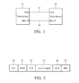
- Fig. 1 is a schematic diagram of an embodiment of a serial data transmission system according to the invention.
- Fig. 2 is a schematic diagram of a data format for the transmission system according to an embodiment of the invention.
- Fig. 3 is a schematic diagram of another embodiment of the data transmission system according to the invention.
- Fig. 4 shows two data formats of two different transmission modes according to an embodiment of the invention.
- Fig. 1 is a schematic diagram of an embodiment of a serial data transmission system according to the invention.
- the serial data transmission system comprises a first device such as a host device 11, a second device such as a slave device 12, a clock signal line 13 and a data line 14.
- the clock signal line 13 is coupled to the clock output terminal SCK of the host device 11 and the clock input terminal CLK of the slave device 12.
- the data line 14 is coupled to the data transmission terminal data_M of the host device 11 and the data transmission terminal data_S of the slave device 12.
- the host device 11 transmits a clock signal to the slave device 12 via the clock signal line 13 such that the host device 11 and the slave device 12 can be synchronized to transmit data therebetween.
- a bitstream can be transmitted via the data line 14 between the host device 11 and the slave device 12.
- the bitstream comprises a plurality of segments, such as a first segment, a second segment and a data segment.
- the first segment can be sent by the host device 11 and comprises at least one bit for indicating a transmission mode and thus representing a mode signal.
- the second segment can also be sent by the host device 11 and comprises at least one bit for indicating the data in the data segment is to be written to the slave device 12 or read from the slave device 12. For example, one bit can be used for indicating a writing operation or a reading operation. If the value of the bit is 0, the data in the data segment is to be written to the slave device 12.
- the bitstream can further comprise a third segment including at least one bit for indicating the state of a storage device, such as a memory, or a writing buffer in the slave device 12.
- the host device 11 can determine, based on the state, whether to write data to the slave device 12.
- the third segment can indicate an address or a state of a storage device in the host device 11 or in the slave device 12, or indicate an instruction.
- the third segment comprises an address for indicating an memory address of a storage device, to which the data to be written into the slave device 12 from the host device 11 will be sent and stored, in the slave device 12, or indicating an memory address of the storage device, at which the data to be written into the slave device 12 from the host device 11 is located, in the host device 11.
- the host device 11 performs a writing operation to the slave device 12
- the data segment is output by the host device 11 and then written to the slave device 12.
- the host device 11 performs a reading operation to the slave device 12
- the data segment is output by the slave device 12 and then written to the host device 11.
- the data segment is arranged after the third segment, and the format of the data in the data segment can be determined based on the first segment.
- Fig. 2 is a schematic diagram of a data format for the transmission system according to an embodiment of the invention.
- the data format includes a first segment 21, a second segment 22, a third segment 23, a fourth segment 24, a fifth segment 25 and a sixth segment 26.
- the first segment 21 comprises at least one bit, which can be sent by a first device, in particular a host device, for indicating a transmission mode and thus representing a mode signal.
- the second segment 22 comprises at least one bit, which represents a read/write signal, for indicating that the host device performs a reading operation or a writing operation to the second device, namely the slave device.
- the second segment 22 can also include a plurality of bits for indicating different writing operations or reading operations.
- the third segment 23 comprises at least one bit for representing a control signal.
- control signal may be only one bit for indicating the state of a storage device, such as a memory, in the host device or the slave device.
- control signal comprises a plurality of bits for indicating different instructions of the host device, and the slave device executes data transmissions or other operations based on the instructions.
- control signal may includes a plurality of bits for representing a start memory address of the storage device, to which the data to be written into the slave device from the host device will be sent and stored, in the slave device, or representing an memory address of the storage device, at which the data to be written into the slave device from the host device is located, in the host device.
- the fourth segment 24 comprises at least one bit, which is sent by the slave device and represents an acknowledge signal.
- the slave device When the slave device receives the control signal from the host device, the slave device sends the acknowledge signal to the host device to inform that the control signal has been received.
- the value of the bit of the acknowledge signal may be "1" or "0".
- the slave device can combine other signal with the acknowledge signal and transmit the combined signal to the host device, wherein the other signal may indicate the state of the storage device of the slave device.
- the fifth segment 25 comprises a plurality of bits for representing a serial data signal and the format of the serial data signal is determined based on the transmission mode of the first segment 21 representing a mode signal. In another embodiment, the format of the serial data signal is further determined based on the control signal of the third segment 23.
- a sixth segment 26 is added.
- the sixth segment 26 comprises at least one bit to represent an interrupt signal INT sent by the slave device.
- the slave device After the host device receives the interrupt signal INT, the slave device operates at an active mode and the data transmission is controlled by the slave device rather than the host device. If the host device does not receive the interrupt signal, the host device operates at an active mode and the control of the data transmission is switched to the host device.
- the host device is an electronic device with a data processing or computing capabilities.
- the host device can be a personal computer, laptop or a personal digital assistant (PDA) and the slave device can be a data access device, such as a digital camera, webcam, ip cam, heartbeat rate monitor, personal pulse indicator or hard disc.
- PDA personal digital assistant
- the electronic device When the electronic device is electrically connected to the data access device, the electronic device first detects whether the data access device outputs an interrupt signal INT. If not, the data access device is controlled by the electronic device. When there is no data to be transmitted between the electronic device and the data access device, the electronic device outputs a control signal to control the data access device to enter a sleep mode so as to save power consumption. When the electronic device detects the interrupt signal INT sent by the data access device, the control of the data transmission between the electronic device and the data access device is switched to the data access device. In this embodiment, the electronic device may operate at a sleep mode or idle mode, and the data access device can transmit a control signal to wake up the electronic device from the sleep mode or the idle mode. In another embodiment, the data access device can wake up the electronic device via internet by a remote control function.
- Fig. 3 is a schematic diagram of another embodiment of the data transmission system according to the invention.
- the data transmission system comprises a first device such as a host device 31, a second device such as a slave device 32, a clock signal line 33 and a data line 34.
- the data lines 33 is coupled between the clock output terminal SCK of the host device 31 and the clock input terminal CLK of the slave device 32.
- the data line 34 is coupled between the data transmission terminal data_M of the host device 31 and the data transmission terminal data_S of the slave device 32.
- the host device 31 transmits a clock signal to the slave device 32 via the clock signal line 33 such that the host device 31 and the slave device 32 can be synchronized to transmit data therebetween.
- a bitstream can be transmitted via the data line 34 between the host device 31 and the slave device 32.
- the host device 31 comprises a first element 37 and a reading buffer 35.
- the slave device 32 comprises a second element 38 and a writing buffer 36.
- the data transmission between the host device 31 and the slave device 32 can be performed under two modes.
- the first mode is a mode for normal data transmission
- the second mode is a mode for rapid data transmission.
- the bitstream 41 When the data transmission between the host device 31 and the slave device 32 is performed under the first mode, the bitstream 41 is applied.
- the bitstream 41 includes a first segment 43a, a second segment 44a, a third segment 45a, a fourth segment 46a and a fifth segment 47a.
- the first segment 43a comprises one bit.
- the value of the bit is 0, the data transmission between the host device 31 and the slave device 32 is performed under the first mode.
- the value of the bit When the value of the bit is 1, the data transmission between the host device 31 and the slave device 32 is performed under the second mode.
- the second segment 44a comprises a read/write (R/W) bit for indicating that the host device 31 performs a reading operation or a writing operation to the slave device 32.
- the host device 31 When the value of the R/W bit is 1, the host device 31 performs the reading operation to read data from the slave device 32. When the value of the R/W bit is 0, the host device 31 performs the writing operation to write data to the slave device 32.
- the third segment 45a indicates a register address, which is sent by the host device 31.
- the host device 31 When the host device 31 writes data to the slave device 32, the host device 31 first writes data to the writing buffer 36 and then sends the register address to the slave device 32. Afterwards, the slave device 32 reads data from the writing buffer 36 and then writes the read data to a register of the second element 38 according to the register address.
- the second element 38 is an LED and the host device 31 writes data to a register of the LED to control the operation of the LED.
- the fourth segment 46a comprises at least one bit which represents an acknowledge signal ACK.
- the slave device 32 receives the address sent by the host device 31, the slave device 32 generates the acknowledge signal ACK for responding to the host device 31.
- the fifth segment 47a comprises a plurality of bits for representing a serial data signal and the format of the serial data signal is determined based on the transmission mode of the first segment 43a.
- the bitstream 42 When the data transmission between the host device 31 and the slave device 32 is performed under the second mode, the bitstream 42 is applied.
- the bitstream 42 includes a first segment 43b, a second segment 44b, a third segment 45b, a fourth segment 46b and a fifth segment 47b.
- the first segment 43b comprises one bit.
- the second segment 44b comprises a read/write (R/W) bit for indicating that the host device 31 performs a reading operation or a writing operation to the slave device 32.
- R/W read/write
- the third segment 45b comprises a state bit for indicating whether the reading buffer 35 or the writing buffer 36 is full.
- the state bit is set to 1
- the host device 31 keeps writing data to the writing buffer 36 until the state bit is set to 1; meanwhile, the slave device 32 reads the data from the writing buffer 36 and writes the read data to the second element 38.
- the writing buffer 36 clears the transmitted data so as to release the memory space for receiving data from the host device 31.
- the host device 31 performs a fast reading operation to the slave device 32 and detects that the value of the state bit is 1, the slave device 32 keeps writing data to the reading buffer 35 until the state bit is set to 0; meanwhile, the host device 31 reads the data from the reading buffer 35 and writes the read data to the first element 37.
- the reading buffer 35 clears the transmitted data so as to release the memory space for receiving data from the slave device 32.
- the fourth segment 46b comprises at least one bit for representing an acknowledge signal ACK.
- the slave device 32 When the slave device 32 receives the state bit sent by the host device 31, the slave device 32 generates the acknowledge signal ACK for responding to the host device 31.
- the fifth segment 47b comprises a plurality of bits for representing a serial data signal and the format of the serial data signal is determined based on the transmission mode of the first segment 43b.
- the slave device 32 responds with an acknowledge signal ACK to the host device 31 after completely receiving a data from the host device 31, and the host device 31 begins to send the next data to the slave device 32 after receiving the acknowledge signal ACK.
- the host device 31 can write data to the writing buffer 36 or read data from the reading buffer 35 without receiving any acknowledge signal ACK for each written or read data so as to increase the data transmission speed.
Landscapes
- Engineering & Computer Science (AREA)
- Computer Networks & Wireless Communication (AREA)
- Signal Processing (AREA)
- Information Transfer Systems (AREA)
Applications Claiming Priority (1)
| Application Number | Priority Date | Filing Date | Title |
|---|---|---|---|
| TW096135054A TWI350457B (en) | 2007-09-19 | 2007-09-19 | Data transmission method and system |
Publications (2)
| Publication Number | Publication Date |
|---|---|
| EP2040410A1 true EP2040410A1 (fr) | 2009-03-25 |
| EP2040410B1 EP2040410B1 (fr) | 2012-02-01 |
Family
ID=40095512
Family Applications (1)
| Application Number | Title | Priority Date | Filing Date |
|---|---|---|---|
| EP08164520A Ceased EP2040410B1 (fr) | 2007-09-19 | 2008-09-17 | Procédé et système de transmission de données |
Country Status (3)
| Country | Link |
|---|---|
| US (1) | US9621334B2 (fr) |
| EP (1) | EP2040410B1 (fr) |
| TW (1) | TWI350457B (fr) |
Families Citing this family (2)
| Publication number | Priority date | Publication date | Assignee | Title |
|---|---|---|---|---|
| JP5840088B2 (ja) * | 2012-07-20 | 2016-01-06 | 株式会社日立ハイテクノロジーズ | 端末通信装置および分散制御システム |
| JP2025538149A (ja) * | 2022-11-07 | 2025-11-26 | キョーセラ・エーブイエックス・コンポーネンツ・(サン・ディエゴ)・インコーポレイテッド | モーダルアンテナを肯定応答で制御するための方法およびシステム |
Citations (6)
| Publication number | Priority date | Publication date | Assignee | Title |
|---|---|---|---|---|
| EP0280391A2 (fr) | 1987-02-24 | 1988-08-31 | Hewlett-Packard Company | Appareil et procédé de transfert d'information |
| EP0377136A2 (fr) * | 1989-01-05 | 1990-07-11 | International Business Machines Corporation | Protocole adaptatif pour liaison de données |
| EP1061453A1 (fr) | 1999-06-15 | 2000-12-20 | Koninklijke Philips Electronics N.V. | Système de transmission et dispositif d'interface entre un système de bus parallèle avec un émetteur récepteur |
| WO2001091407A1 (fr) | 2000-05-25 | 2001-11-29 | Soma Networks, Inc. | Voie de communication de donnees dependante de la qualite |
| US20070064735A1 (en) | 2005-09-02 | 2007-03-22 | Broadcom Corporation, A California Corporation | Robust high-throughput frame for low-quality wireless channel conditions |
| EP1860815A1 (fr) * | 2006-05-24 | 2007-11-28 | High Tech Computer Corp. | Procédé de transmission de données et son circuit de transmission |
Family Cites Families (20)
| Publication number | Priority date | Publication date | Assignee | Title |
|---|---|---|---|---|
| US5255376A (en) * | 1992-01-14 | 1993-10-19 | Sun Microsystems, Inc. | Method and apparatus for supporting a dual bit length protocol for data transfers |
| KR970006027B1 (ko) * | 1992-08-17 | 1997-04-23 | 마쯔시다 덴기 산교 가부시끼가이샤 | 데이터전송장치 및 멀티프로세서시스템 |
| US5686913A (en) * | 1995-10-06 | 1997-11-11 | Analog Devices, Inc. | Serial data interface apparatus and method for detecting an input word length and selecting an operating mode accordingly |
| CN1155628C (zh) | 1995-12-01 | 2004-06-30 | 智索股份有限公司 | 树脂制品 |
| JP2000285069A (ja) | 1999-03-31 | 2000-10-13 | Copyer Co Ltd | 同期式シリアル通信方法及び同期式シリアル通信システム |
| DE19917576A1 (de) | 1999-04-19 | 2000-10-26 | Moeller Gmbh | Datenübertragungseinrichtung |
| US6553336B1 (en) * | 1999-06-25 | 2003-04-22 | Telemonitor, Inc. | Smart remote monitoring system and method |
| US6765969B1 (en) * | 1999-09-01 | 2004-07-20 | Motorola, Inc. | Method and device for multi-user channel estimation |
| US6362781B1 (en) * | 2000-06-30 | 2002-03-26 | Motorola, Inc. | Method and device for adaptive antenna combining weights |
| US6778622B2 (en) * | 2000-12-18 | 2004-08-17 | Schlumberger Technology Corporation | Estimating timing error in samples of a discrete multitone modulated signal |
| US6799235B2 (en) * | 2002-01-02 | 2004-09-28 | Intel Corporation | Daisy chain latency reduction |
| US7139340B2 (en) * | 2002-06-28 | 2006-11-21 | Hitachi, Ltd. | Robust OFDM carrier recovery methods and apparatus |
| TWI236264B (en) * | 2002-09-05 | 2005-07-11 | Winbond Electronics Corp | Single wire serial communication protocol method and circuit |
| US7379517B1 (en) * | 2003-05-23 | 2008-05-27 | Xilinx, Inc | Method and apparatus for signaling characteristics of a transmitted signal |
| US20050083930A1 (en) * | 2003-10-20 | 2005-04-21 | Jen-Kai Chen | Method of early buffer release and associated MAC controller |
| US20050163263A1 (en) * | 2004-01-28 | 2005-07-28 | Gupta Alok K. | Systems and methods for frequency acquisition in a wireless communication network |
| WO2005101773A1 (fr) * | 2004-04-16 | 2005-10-27 | Thine Electronics, Inc. | Circuit emetteur, circuit recepteur, circuit d'extraction d'horloge, procede de transmission de donnees et systeme de transmission de donnees |
| KR20050103099A (ko) * | 2004-04-24 | 2005-10-27 | 삼성전자주식회사 | 이동통신 시스템에서 방송 서비스 제공 장치 및 방법 |
| US20060025079A1 (en) * | 2004-08-02 | 2006-02-02 | Ilan Sutskover | Channel estimation for a wireless communication system |
| US8730877B2 (en) * | 2005-06-16 | 2014-05-20 | Qualcomm Incorporated | Pilot and data transmission in a quasi-orthogonal single-carrier frequency division multiple access system |
-
2007
- 2007-09-19 TW TW096135054A patent/TWI350457B/zh not_active IP Right Cessation
-
2008
- 2008-09-17 EP EP08164520A patent/EP2040410B1/fr not_active Ceased
- 2008-09-17 US US12/212,418 patent/US9621334B2/en not_active Expired - Fee Related
Patent Citations (6)
| Publication number | Priority date | Publication date | Assignee | Title |
|---|---|---|---|---|
| EP0280391A2 (fr) | 1987-02-24 | 1988-08-31 | Hewlett-Packard Company | Appareil et procédé de transfert d'information |
| EP0377136A2 (fr) * | 1989-01-05 | 1990-07-11 | International Business Machines Corporation | Protocole adaptatif pour liaison de données |
| EP1061453A1 (fr) | 1999-06-15 | 2000-12-20 | Koninklijke Philips Electronics N.V. | Système de transmission et dispositif d'interface entre un système de bus parallèle avec un émetteur récepteur |
| WO2001091407A1 (fr) | 2000-05-25 | 2001-11-29 | Soma Networks, Inc. | Voie de communication de donnees dependante de la qualite |
| US20070064735A1 (en) | 2005-09-02 | 2007-03-22 | Broadcom Corporation, A California Corporation | Robust high-throughput frame for low-quality wireless channel conditions |
| EP1860815A1 (fr) * | 2006-05-24 | 2007-11-28 | High Tech Computer Corp. | Procédé de transmission de données et son circuit de transmission |
Also Published As
| Publication number | Publication date |
|---|---|
| US9621334B2 (en) | 2017-04-11 |
| EP2040410B1 (fr) | 2012-02-01 |
| TW200915086A (en) | 2009-04-01 |
| US20090074122A1 (en) | 2009-03-19 |
| TWI350457B (en) | 2011-10-11 |
Similar Documents
| Publication | Publication Date | Title |
|---|---|---|
| US7328399B2 (en) | Synchronous serial data communication bus | |
| TWI417703B (zh) | 相容於通用序列匯流排協定之時脈同步方法 | |
| US8285557B2 (en) | Apparatus, system and method for buffering audio data to allow low power states in a processing system during audio playback | |
| US20110208913A1 (en) | Storage device and storage system | |
| EP2857930A2 (fr) | Techniques de transmission de commandes vers un dispositif cible | |
| US8494010B2 (en) | Data transfer device, data transmitting device, data receiving device, and data transfer method | |
| EP2207101A1 (fr) | Procédé et dispositif pour une interface parallèle | |
| US7779194B2 (en) | Data modification module | |
| JP4186940B2 (ja) | データ転送制御装置及び電子機器 | |
| JP3780419B2 (ja) | データ転送制御装置及び電子機器 | |
| EP2040410B1 (fr) | Procédé et système de transmission de données | |
| EP1160671A2 (fr) | Circuit d'interface d'ordinateur central | |
| JP2008117157A (ja) | 半導体メモリカード、ホスト装置、及びデータ転送方法 | |
| CN101436172B (zh) | 数据传输方法与系统 | |
| EP0382342B1 (fr) | Transmission DMA pour système ordinateur | |
| CN114564441B (zh) | 片上系统、数据处理方法及计算机设备 | |
| JP2008041022A (ja) | I/o装置、通信装置、サーボモータ制御装置、制御システムおよびロボットシステム | |
| Lawrence | MIPI high speed serial interface standard for mobile displays | |
| JP2000276435A (ja) | データ転送装置及びデータ転送方法 | |
| KR101345437B1 (ko) | 칩들간의 통신을 위한 인터페이스 장치 및 방법 | |
| US20220309009A1 (en) | Methods of controlling power consumption, boards, electronic devices and storage media | |
| US20070005834A1 (en) | Memory chips with buffer circuitry | |
| CN114880270A (zh) | Spi设备及其数据传输方法 | |
| KR100265056B1 (ko) | 프로세서와직렬입/출력제어기간의인터페이스장치및그방법 | |
| CN101211328B (zh) | 高性能可编程逻辑系统接口及芯片 |
Legal Events
| Date | Code | Title | Description |
|---|---|---|---|
| PUAI | Public reference made under article 153(3) epc to a published international application that has entered the european phase |
Free format text: ORIGINAL CODE: 0009012 |
|
| AK | Designated contracting states |
Kind code of ref document: A1 Designated state(s): AT BE BG CH CY CZ DE DK EE ES FI FR GB GR HR HU IE IS IT LI LT LU LV MC MT NL NO PL PT RO SE SI SK TR |
|
| AX | Request for extension of the european patent |
Extension state: AL BA MK RS |
|
| 17P | Request for examination filed |
Effective date: 20090922 |
|
| 17Q | First examination report despatched |
Effective date: 20091016 |
|
| AKX | Designation fees paid |
Designated state(s): DE FR GB NL |
|
| RAP1 | Party data changed (applicant data changed or rights of an application transferred) |
Owner name: HTC CORPORATION |
|
| GRAP | Despatch of communication of intention to grant a patent |
Free format text: ORIGINAL CODE: EPIDOSNIGR1 |
|
| GRAS | Grant fee paid |
Free format text: ORIGINAL CODE: EPIDOSNIGR3 |
|
| GRAA | (expected) grant |
Free format text: ORIGINAL CODE: 0009210 |
|
| AK | Designated contracting states |
Kind code of ref document: B1 Designated state(s): DE FR GB NL |
|
| REG | Reference to a national code |
Ref country code: GB Ref legal event code: FG4D |
|
| REG | Reference to a national code |
Ref country code: NL Ref legal event code: T3 |
|
| REG | Reference to a national code |
Ref country code: DE Ref legal event code: R096 Ref document number: 602008013037 Country of ref document: DE Effective date: 20120329 |
|
| PLBE | No opposition filed within time limit |
Free format text: ORIGINAL CODE: 0009261 |
|
| STAA | Information on the status of an ep patent application or granted ep patent |
Free format text: STATUS: NO OPPOSITION FILED WITHIN TIME LIMIT |
|
| 26N | No opposition filed |
Effective date: 20121105 |
|
| REG | Reference to a national code |
Ref country code: DE Ref legal event code: R097 Ref document number: 602008013037 Country of ref document: DE Effective date: 20121105 |
|
| REG | Reference to a national code |
Ref country code: FR Ref legal event code: PLFP Year of fee payment: 9 |
|
| REG | Reference to a national code |
Ref country code: FR Ref legal event code: PLFP Year of fee payment: 10 |
|
| REG | Reference to a national code |
Ref country code: FR Ref legal event code: PLFP Year of fee payment: 11 |
|
| PGFP | Annual fee paid to national office [announced via postgrant information from national office to epo] |
Ref country code: FR Payment date: 20180813 Year of fee payment: 11 Ref country code: DE Payment date: 20180904 Year of fee payment: 11 |
|
| PGFP | Annual fee paid to national office [announced via postgrant information from national office to epo] |
Ref country code: NL Payment date: 20180912 Year of fee payment: 11 Ref country code: GB Payment date: 20180912 Year of fee payment: 11 |
|
| REG | Reference to a national code |
Ref country code: DE Ref legal event code: R119 Ref document number: 602008013037 Country of ref document: DE |
|
| REG | Reference to a national code |
Ref country code: NL Ref legal event code: MM Effective date: 20191001 |
|
| PG25 | Lapsed in a contracting state [announced via postgrant information from national office to epo] |
Ref country code: DE Free format text: LAPSE BECAUSE OF NON-PAYMENT OF DUE FEES Effective date: 20200401 Ref country code: NL Free format text: LAPSE BECAUSE OF NON-PAYMENT OF DUE FEES Effective date: 20191001 |
|
| GBPC | Gb: european patent ceased through non-payment of renewal fee |
Effective date: 20190917 |
|
| PG25 | Lapsed in a contracting state [announced via postgrant information from national office to epo] |
Ref country code: FR Free format text: LAPSE BECAUSE OF NON-PAYMENT OF DUE FEES Effective date: 20190930 Ref country code: GB Free format text: LAPSE BECAUSE OF NON-PAYMENT OF DUE FEES Effective date: 20190917 |