EP2040457A2 - Bolometerartiger ungekühlter Infrarotstrahlsensor und Ansteuerungsverfahren dafür - Google Patents
Bolometerartiger ungekühlter Infrarotstrahlsensor und Ansteuerungsverfahren dafür Download PDFInfo
- Publication number
- EP2040457A2 EP2040457A2 EP08015926A EP08015926A EP2040457A2 EP 2040457 A2 EP2040457 A2 EP 2040457A2 EP 08015926 A EP08015926 A EP 08015926A EP 08015926 A EP08015926 A EP 08015926A EP 2040457 A2 EP2040457 A2 EP 2040457A2
- Authority
- EP
- European Patent Office
- Prior art keywords
- image pickup
- voltage
- pickup region
- row selection
- signal
- Prior art date
- Legal status (The legal status is an assumption and is not a legal conclusion. Google has not performed a legal analysis and makes no representation as to the accuracy of the status listed.)
- Withdrawn
Links
Images





Classifications
-
- G—PHYSICS
- G01—MEASURING; TESTING
- G01J—MEASUREMENT OF INTENSITY, VELOCITY, SPECTRAL CONTENT, POLARISATION, PHASE OR PULSE CHARACTERISTICS OF INFRARED, VISIBLE OR ULTRAVIOLET LIGHT; COLORIMETRY; RADIATION PYROMETRY
- G01J5/00—Radiation pyrometry, e.g. infrared or optical thermometry
- G01J5/10—Radiation pyrometry, e.g. infrared or optical thermometry using electric radiation detectors
- G01J5/20—Radiation pyrometry, e.g. infrared or optical thermometry using electric radiation detectors using resistors, thermistors or semiconductors sensitive to radiation, e.g. photoconductive devices
-
- G—PHYSICS
- G01—MEASURING; TESTING
- G01J—MEASUREMENT OF INTENSITY, VELOCITY, SPECTRAL CONTENT, POLARISATION, PHASE OR PULSE CHARACTERISTICS OF INFRARED, VISIBLE OR ULTRAVIOLET LIGHT; COLORIMETRY; RADIATION PYROMETRY
- G01J5/00—Radiation pyrometry, e.g. infrared or optical thermometry
- G01J5/10—Radiation pyrometry, e.g. infrared or optical thermometry using electric radiation detectors
- G01J5/20—Radiation pyrometry, e.g. infrared or optical thermometry using electric radiation detectors using resistors, thermistors or semiconductors sensitive to radiation, e.g. photoconductive devices
- G01J5/22—Electrical features thereof
-
- G—PHYSICS
- G01—MEASURING; TESTING
- G01J—MEASUREMENT OF INTENSITY, VELOCITY, SPECTRAL CONTENT, POLARISATION, PHASE OR PULSE CHARACTERISTICS OF INFRARED, VISIBLE OR ULTRAVIOLET LIGHT; COLORIMETRY; RADIATION PYROMETRY
- G01J5/00—Radiation pyrometry, e.g. infrared or optical thermometry
- G01J5/80—Calibration
-
- H—ELECTRICITY
- H04—ELECTRIC COMMUNICATION TECHNIQUE
- H04N—PICTORIAL COMMUNICATION, e.g. TELEVISION
- H04N25/00—Circuitry of solid-state image sensors [SSIS]; Control thereof
- H04N25/60—Noise processing, e.g. detecting, correcting, reducing or removing noise
- H04N25/616—Noise processing, e.g. detecting, correcting, reducing or removing noise involving a correlated sampling function, e.g. correlated double sampling [CDS] or triple sampling
-
- H—ELECTRICITY
- H04—ELECTRIC COMMUNICATION TECHNIQUE
- H04N—PICTORIAL COMMUNICATION, e.g. TELEVISION
- H04N25/00—Circuitry of solid-state image sensors [SSIS]; Control thereof
- H04N25/60—Noise processing, e.g. detecting, correcting, reducing or removing noise
- H04N25/65—Noise processing, e.g. detecting, correcting, reducing or removing noise applied to reset noise, e.g. KTC noise related to CMOS structures by techniques other than CDS
-
- H—ELECTRICITY
- H04—ELECTRIC COMMUNICATION TECHNIQUE
- H04N—PICTORIAL COMMUNICATION, e.g. TELEVISION
- H04N25/00—Circuitry of solid-state image sensors [SSIS]; Control thereof
- H04N25/60—Noise processing, e.g. detecting, correcting, reducing or removing noise
- H04N25/67—Noise processing, e.g. detecting, correcting, reducing or removing noise applied to fixed-pattern noise, e.g. non-uniformity of response
-
- H—ELECTRICITY
- H04—ELECTRIC COMMUNICATION TECHNIQUE
- H04N—PICTORIAL COMMUNICATION, e.g. TELEVISION
- H04N25/00—Circuitry of solid-state image sensors [SSIS]; Control thereof
- H04N25/60—Noise processing, e.g. detecting, correcting, reducing or removing noise
- H04N25/67—Noise processing, e.g. detecting, correcting, reducing or removing noise applied to fixed-pattern noise, e.g. non-uniformity of response
- H04N25/671—Noise processing, e.g. detecting, correcting, reducing or removing noise applied to fixed-pattern noise, e.g. non-uniformity of response for non-uniformity detection or correction
Definitions
- the present invention relates to a bolometer type uncooled infrared ray sensor and its driving method.
- Image sensors utilizing infrared rays have features that they can pick up images night and day and the infrared rays are higher in permeability through smoke or fog than visible light.
- the image sensors utilizing infrared rays have a feature that temperature information of a subject can also be obtained. Therefore, the image sensors utilizing infrared rays have a wide application range as surveillance cameras and fire sensing cameras not to speak of the defense field.
- a greatest drawback of quantum type infrared ray solid image pickup devices which are conventional mainstream devices is that a cooling mechanism for low temperature operation is needed.
- uncooled infrared ray image sensors which do not need such a cooling mechanism have been developed (see, for example, Japanese Patent No. 3793033 ).
- the infrared ray image sensors are insufficient in sensitivity and dynamic range as compared with image sensors utilizing visible rays.
- sensors having a NETD (Noise Equivalent Temperature Difference) of approximately 0.1 K and a dynamic range of approximately 30 K are needed. Development of a sensor having enhanced output linearity, a higher sensitivity and a wider dynamic range is anticipated.
- noise generated in image sensors can be broadly classified into random noise and fixed pattern noise.
- the random noise there are 1/f noise having a power spectrum which is in inverse proportion to the frequency f and kTC noise which is thermal noise caused by capacitance.
- the fixed pattern noise is caused mainly by characteristic variations of diodes and threshold variations of transistors.
- the noise can be canceled in principle by finding a difference between a signal voltage and a reference signal before and after resetting.
- a correlated double sampling (CDS) circuit with an electrical reset switch is typically used in visible region image sensors using photodiodes.
- CDS correlated double sampling
- thermal sensors using a bolometer a thermal reset mechanism must be fabricated, making the CDS circuit unpractical.
- the present invention has been made in view of these circumstances, and an object of thereof is to provide a bolometer type uncooled infrared ray sensor and its driving method capable of reducing the fixed pattern noise and 1/f noise without fabricating a thermal reset mechanism.
- a bolometer type uncooled infrared ray sensor including: an image pickup region having detection pixels arranged in a matrix form on a semiconductor substrate to detect incident infrared rays, each of the detection pixels being formed of one or more diodes connected in series; a plurality of row selection lines provided in the image pickup region so as to respectively correspond to rows of the detection pixels and connected to anodes of the diodes in the respectively corresponding rows; current sources capable of letting constant currents flow through the respective row selection lines; a plurality of signal lines provided in the image pickup region so as to respectively correspond to columns of the detection pixels and connected to cathodes of the diodes in the respectively corresponding columns; voltage readout circuits provided so as to respectively correspond to the signal lines to read out signal voltages generated on the respectively corresponding signal lines; coupling capacitances respectively provided between the respective signal lines and the corresponding voltage readout circuits; and a calculator which calculates a difference between two signal voltages read out by the voltage
- a bolometer type uncooled infrared ray sensor including: an image pickup region having detection pixels arranged in a matrix form on a semiconductor substrate to detect incident infrared rays, each of the detection pixels being formed of one or more diodes connected in series; a plurality of row selection lines provided in the image pickup region so as to respectively correspond to rows of the detection pixels and connected to anodes of the diodes in the respectively corresponding rows; current sources capable of letting constant currents flow through the respective row selection lines; a plurality of signal lines provided in the image pickup region so as to respectively correspond to columns of the detection pixels and connected to cathodes of the diodes in the respectively corresponding columns; one row of non-sensitivity pixels having no infrared ray sensitivity disposed in the image pickup region in a direction of the rows; and voltage readout circuits provided so as to respectively correspond to the signal lines to read out a difference between signal voltages generated on the respectively corresponding signal lines and output of the non-sensitivity
- a drive method for a bolometer type uncooled infrared ray sensor including an image pickup region having detection pixels arranged in a matrix form on a semiconductor substrate to detect incident infrared rays, each of the detection pixels being formed of one or more diodes connected in series; a plurality of row selection lines provided in the image pickup region so as to respectively correspond to rows of the detection pixels and connected to anodes of the diodes in the respectively corresponding rows; current sources capable of letting constant currents flow through the respective row selection lines; and a plurality of signal lines provided in the image pickup region so as to respectively correspond to columns of the detection pixels and connected to cathodes of the diodes in the respectively corresponding columns, the drive method comprising: selecting one row selection line from the row selection lines; letting flow a first bias current through the diodes connected to the selected row selection line; reading out and retaining a first voltage generated on the corresponding signal
- Infrared rays emitted from an object are focused by an optical lens disposed in front of a sensor to raise the temperature of a diode formed of silicon installed in a hollow region so as to prevent heat from escaping to the outside.
- a Ge lens having a transmittance of 90% in a wavelength region of 8 to 12 ⁇ m and an F value of 1.0 is used, a temperature rise of the diode per 1 K of the object becomes approximately 1 mK.
- a constant current I s is let flow through the diode by a constant current source 8.
- Equation (1) I s ⁇ exp qV / kT
- I s A ⁇ exp - E g / kT
- Equation (3) is a band gap of silicon (approximately 1.11 eV).
- I A ⁇ exp - E g / kT ⁇ exp qV / kT is obtained.
- FIG. 5 shows a graph of the temperature coefficient of the diode.
- the temperature coefficient becomes equal to approximately -1.5 mV/K.
- the temperature coefficient becomes approximately -2 mV/K.
- Equation (10) the present inventors have found the following fact. If readout is conducted a plurality of times for current values differing in operating point, it becomes possible to cancel the bias component and self heating component contained in V d and only a signal component can be extracted. As a result, it becomes possible to remove fixed pattern noise, 1/f noise and reset noise caused by variations of the diode.
- FIG. 1 A circuit of a bolometer type uncooled infrared ray sensor according to a first embodiment of the present invention is shown in FIG. 1 .
- a 2 by 2 pixel configuration having two rows by two columns is shown to simplify the description.
- the circuit can be applied to an m by n pixel configuration having more rows by more columns.
- a plurality of row selection lines 4 1 and 4 2 and a plurality of vertical signal lines 5 1 and 5 2 are disposed.
- a row selection circuit 40 and a horizontal selection circuit 6 are disposed in the row direction and the column direction of the image pickup region, respectively.
- the row selection lines 4 1 and 4 2 are connected to the row selection circuit 40, and horizontal selection lines 7 1 and 7 2 are connected to the horizontal selection circuit 6.
- load MOS transistors 8 1 and 8 2 are connected to the vertical signal lines 5 of respective columns.
- a substrate voltage GL1_V ss is applied to sources of the load MOS transistors 8 1 and 8 2
- a gate control voltage GL1 is applied to gates of the load MOS transistors 8 1 and 8 2 .
- a power supply voltage V 1 is applied to a row selection line (for example, 4 1 ) selected by the row selection circuit 40, whereas V 2 is applied to a row selection line (for example, 4 2 ) which is not selected by the row selection circuit 40.
- V 1 is applied to a row selection line (for example, 4 1 ) selected by the row selection circuit 40
- V 2 is applied to a row selection line (for example, 4 2 ) which is not selected by the row selection circuit 40.
- 5 ⁇ 10 -3 is supposed.
- This noise value is as low as approximately 1/80 of noise of a CMOS sensor which is a visible ray image sensor of MOS type.
- a reset signal VRST is applied to the reset transistor 13 j at its gate, and a voltage VRS is applied to the reset transistor 13 j at its source.
- An output reset transistor 33 is connected at its drain to the output signal line 24.
- a control signal HRST is applied to the output reset transistor 33 at its gate.
- a control signal HRS is applied to the output reset transistor 33 at its source.
- a memory 50 and a difference calculator 60 are connected to the output signal line 24.
- the gate and drain of the amplifying transistor 10 j are made to have the same potential by turning on the sample transistor 15 j .
- one diode is connected.
- the sensitivity to the incident infrared rays can be increased by connecting a plurality of diodes.
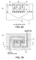
- FIGS. 2A and 2B respectively show a section structure and a plan structure of the infrared ray detection pixel in the infrared ray sensor according to the present embodiment.
- a sensor part 16 including a pn junction for thermoelectric conversion includes an infrared ray absorption layer 22, a pn junction within a SOI layer 19 formed for thermoelectric conversion, and a silicon oxide film layer 20 supporting the SOI layer 19, which are formed on a hollow structure 18 formed within a single crystal silicon supporting substrate 17.
- a supporting part 21 is provided to support the sensor part 16 on the hollow structure 18 and output an electric signal supplied from the sensor part 16.
- a connection part (not illustrated) is provided to connect the sensor part 16 to the vertical signal lines 5 1 and 5 2 and the row selection lines 4 1 and 4 2 .
- FIGS. 2A and 2B show a structure in the case where two pn junctions are connected in series.
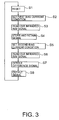
- FIG. 3 shows a procedure of the drive method for the infrared ray sensor according to the present embodiment.
- FIG. 4 shows its timing chart.
- readout is conducted a plurality of times for current values differing in operating point.
- step S1 in FIG. 3 reset is conducted as represented in step S1 in FIG. 3 .
- a row selection line (for example, the row selection line 4 1 ) is selected by the row selection circuit 40, and a first bias current condition is set on the selected row selection line (step S2).
- the source voltage and the gate voltage Vg of the amplifying transistor 10 j are set equal to V hamp and V hamp + V th , respectively.
- V hamp is a voltage of the control signal HAMP
- V th is a threshold voltage of the amplifying transistor 10 j .
- infrared ray signal readout is conducted, and the signal thus read out is stored and retained (steps S3 and S4).
- a constant current I flows through the diodes by suitably choosing the value of the gate voltage of the load transistor 8 j .
- the quantity of charge can be controlled by suitably setting the voltage V hamp of the control signal HAMP.
- a second bias current condition which differs in operating point from the first bias current condition is set on the selected row selection line (step S5).
- Infrared ray signal readout is conducted in the same way as the foregoing description (see a readout time period 102 shown in FIG. 4 ).
- the potential V out ' of the storage capacitance 12 j caused by a change ⁇ V d ' of voltage drop across the diodes is read (step S6).
- the difference calculator 60 finds a difference between the potential V out ' and the potential V out at the operating point under the first bias current condition stored in the memory 50 (step S7). As a result, an infrared ray signal having little noise can be obtained (step S8).
- the process of the steps 1 to 8 is conducted for respective selected row lines successively.
- a control voltage Vs1 is an output voltage of the diodes.
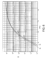
- Results obtained by conducting simulation on operating points under the first and second bias current conditions are shown in FIG. 6 .
- the axis of abscissas indicates a voltage VF between the anode and cathode of the diodes, and the axis of ordinates indicates a current I which flows through the diodes.
- a graph g 1 indicates I-V characteristics of a diode at a room temperature 300 K.
- a graph g 2 indicates I-V characteristics of the diode at 310 K. The change ⁇ V d of voltage drop across the diode at the operating point under the first bias current condition and the change ⁇ V d ' of the voltage drop across the diode at the operating point under the second bias current condition are exhibited.
- FIG. 7 A resultant waveform diagram is shown in FIG. 7 .
- readout time periods 100 and 102 are time periods for conducting readout from reference cells 2 (see FIG. 9 ) whereas readout time periods 101 and 103 are time periods for conducting readout from pixel cells 1. Readout from reference cells 2 and readout from pixel cells 1 are conducted alternately.
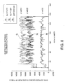
- An infrared ray sensor which includes twelve pixels in each row is created. Signals and a difference between them which are obtained by experimentally finding data (gradient after A/D transformation) of corresponding to one row of pixels (corresponding to 12 bits) with respect to two bias current values of the infrared ray sensor are shown in FIG. 8 .
- a graph g 3 is a signal waveform diagram indicating the difference between them. Values of standard deviation ⁇ indicating variations of the graphs g 1 and g 2 are 951 and 905, respectively. A value of standard deviation ⁇ indicating variations of the graph g 3 is 450. It is appreciated from this that the variations can be suppressed to approximately half by obtaining the difference between the signals.
- the fixed pattern noise and 1/f noise can be reduced without fabricating the thermal reset mechanism as heretofore described.
- FIG. 9 A circuit of a bolometer type uncooled infrared ray sensor according to a second embodiment of the present invention is shown in FIG. 9 .
- differential amplifiers (operational amplifiers) 41 j (j 1, 2) instead, disposing one row of reference cells each formed of a non-sensitivity pixel 2 having no infrared ray sensitivity in the image pickup region 3, disposing a reference vertical signal line 5 0 connected to those reference cells, and a load MOS transistor 8 0 connected to the reference vertical signal line 5 0 .
- a substrate voltage GL1_V SS is applied to the load MOS transistor 8 0 at its source, and a gate control voltage GL1 is applied to the load MOS transistors 8 0 at its gate.
- the fixed pattern noise and 1/f noise can be reduced without fabricating the thermal reset mechanism in the same way as the first embodiment.
- control signals can be reduced remarkably as compared with the first embodiment because differential amplifiers 41 are used instead of the amplifying readout circuits each including a plurality of transistors.
- a bolometer type uncooled infrared ray sensor with the fixed pattern noise and 1/f noise reduced without fabricating the thermal reset mechanism can be provided as heretofore described.
Landscapes
- Engineering & Computer Science (AREA)
- Multimedia (AREA)
- Signal Processing (AREA)
- Physics & Mathematics (AREA)
- General Physics & Mathematics (AREA)
- Spectroscopy & Molecular Physics (AREA)
- Photometry And Measurement Of Optical Pulse Characteristics (AREA)
- Transforming Light Signals Into Electric Signals (AREA)
Applications Claiming Priority (1)
| Application Number | Priority Date | Filing Date | Title |
|---|---|---|---|
| JP2007243632A JP2009074898A (ja) | 2007-09-20 | 2007-09-20 | ボロメータ型非冷却赤外線センサおよびその駆動方法 |
Publications (2)
| Publication Number | Publication Date |
|---|---|
| EP2040457A2 true EP2040457A2 (de) | 2009-03-25 |
| EP2040457A3 EP2040457A3 (de) | 2010-09-29 |
Family
ID=40134938
Family Applications (1)
| Application Number | Title | Priority Date | Filing Date |
|---|---|---|---|
| EP08015926A Withdrawn EP2040457A3 (de) | 2007-09-20 | 2008-09-10 | Bolometerartiger ungekühlter Infrarotstrahlsensor und Ansteuerungsverfahren dafür |
Country Status (3)
| Country | Link |
|---|---|
| US (1) | US7737400B2 (de) |
| EP (1) | EP2040457A3 (de) |
| JP (1) | JP2009074898A (de) |
Cited By (1)
| Publication number | Priority date | Publication date | Assignee | Title |
|---|---|---|---|---|
| MD340Z (ro) * | 2010-04-23 | 2011-09-30 | Институт Электронной Инженерии И Промышленных Технологий | Bolometru |
Families Citing this family (4)
| Publication number | Priority date | Publication date | Assignee | Title |
|---|---|---|---|---|
| JP2011187594A (ja) * | 2010-03-08 | 2011-09-22 | Hitachi Displays Ltd | フォトセンサ装置 |
| JP5143176B2 (ja) * | 2010-03-31 | 2013-02-13 | 株式会社東芝 | 赤外線撮像素子およびその製造方法 |
| KR101195390B1 (ko) * | 2010-11-12 | 2012-10-30 | 에스케이하이닉스 주식회사 | 적외선 신호 검출 회로 및 적외선 신호 검출 방법 |
| FR3009388B1 (fr) * | 2013-07-30 | 2015-07-17 | Ulis | Diagnostic de l'etat defectueux d'une matrice de detection bolometrique |
Citations (1)
| Publication number | Priority date | Publication date | Assignee | Title |
|---|---|---|---|---|
| JP3793033B2 (ja) | 2001-03-29 | 2006-07-05 | 株式会社東芝 | 赤外線センサ及びその駆動方法 |
Family Cites Families (9)
| Publication number | Priority date | Publication date | Assignee | Title |
|---|---|---|---|---|
| JPH04175622A (ja) * | 1990-11-08 | 1992-06-23 | Mitsubishi Electric Corp | 温度検出回路 |
| US5419637A (en) * | 1993-11-03 | 1995-05-30 | Santa Barbara Research Center | Method and apparatus for measuring temperature using an inherently calibrated p-n junction-type temperature sensor |
| JP2001215152A (ja) * | 2000-02-03 | 2001-08-10 | Mitsubishi Electric Corp | 赤外線固体撮像素子 |
| JP3497797B2 (ja) * | 2000-03-30 | 2004-02-16 | 株式会社東芝 | 赤外線センサの製造方法 |
| US6759657B2 (en) * | 2001-03-27 | 2004-07-06 | Kabushiki Kaisha Toshiba | Infrared sensor |
| JP3866069B2 (ja) * | 2001-09-26 | 2007-01-10 | 株式会社東芝 | 赤外線固体撮像装置 |
| JP3616622B2 (ja) * | 2002-08-26 | 2005-02-02 | 株式会社東芝 | 赤外線撮像装置 |
| JP4257994B2 (ja) * | 2004-12-15 | 2009-04-30 | 三菱電機株式会社 | 赤外線撮像素子と赤外線センサ |
| JP5127278B2 (ja) * | 2007-04-05 | 2013-01-23 | 三菱電機株式会社 | 熱型赤外線固体撮像素子及び赤外線カメラ |
-
2007
- 2007-09-20 JP JP2007243632A patent/JP2009074898A/ja active Pending
-
2008
- 2008-09-08 US US12/206,234 patent/US7737400B2/en not_active Expired - Fee Related
- 2008-09-10 EP EP08015926A patent/EP2040457A3/de not_active Withdrawn
Patent Citations (1)
| Publication number | Priority date | Publication date | Assignee | Title |
|---|---|---|---|---|
| JP3793033B2 (ja) | 2001-03-29 | 2006-07-05 | 株式会社東芝 | 赤外線センサ及びその駆動方法 |
Cited By (1)
| Publication number | Priority date | Publication date | Assignee | Title |
|---|---|---|---|---|
| MD340Z (ro) * | 2010-04-23 | 2011-09-30 | Институт Электронной Инженерии И Промышленных Технологий | Bolometru |
Also Published As
| Publication number | Publication date |
|---|---|
| US20090095909A1 (en) | 2009-04-16 |
| EP2040457A3 (de) | 2010-09-29 |
| JP2009074898A (ja) | 2009-04-09 |
| US7737400B2 (en) | 2010-06-15 |
Similar Documents
| Publication | Publication Date | Title |
|---|---|---|
| US6770881B2 (en) | Infrared sensor | |
| JP5127278B2 (ja) | 熱型赤外線固体撮像素子及び赤外線カメラ | |
| US7943905B2 (en) | Infrared solid-state image sensor | |
| US6809320B2 (en) | Solid-state infrared imager | |
| US8344321B2 (en) | Infrared imaging device | |
| US7361899B2 (en) | Infrared sensor, infrared camera, method of driving infrared sensor, and method of driving infrared camera | |
| US7535003B2 (en) | Solid-state imaging device and driving method thereof | |
| JP2993557B2 (ja) | 熱型赤外線撮像装置およびその駆動方法 | |
| JP5685927B2 (ja) | 赤外線検出回路、センサーデバイス及び電子機器 | |
| EP2642261A1 (de) | Ungekühlte Infrarotabbildungsvorrichtung | |
| US7737400B2 (en) | Bolometer type uncooled infrared ray sensor and method for driving the same | |
| US9222838B2 (en) | Detection device, sensor device, and electronic device | |
| JP6701881B2 (ja) | 撮像装置、赤外線検出装置、及び赤外線検出器の暗電流の補正方法 | |
| JP4153861B2 (ja) | 赤外線センサ | |
| JP4343144B2 (ja) | 赤外線センサ | |
| JP3657885B2 (ja) | 赤外線センサ装置およびその駆動方法 | |
| JP3648506B2 (ja) | 赤外線撮像装置 | |
| JP4331160B2 (ja) | 赤外線センサおよびその駆動方法 |
Legal Events
| Date | Code | Title | Description |
|---|---|---|---|
| PUAI | Public reference made under article 153(3) epc to a published international application that has entered the european phase |
Free format text: ORIGINAL CODE: 0009012 |
|
| 17P | Request for examination filed |
Effective date: 20080910 |
|
| AK | Designated contracting states |
Kind code of ref document: A2 Designated state(s): AT BE BG CH CY CZ DE DK EE ES FI FR GB GR HR HU IE IS IT LI LT LU LV MC MT NL NO PL PT RO SE SI SK TR |
|
| AX | Request for extension of the european patent |
Extension state: AL BA MK RS |
|
| PUAL | Search report despatched |
Free format text: ORIGINAL CODE: 0009013 |
|
| AK | Designated contracting states |
Kind code of ref document: A3 Designated state(s): AT BE BG CH CY CZ DE DK EE ES FI FR GB GR HR HU IE IS IT LI LT LU LV MC MT NL NO PL PT RO SE SI SK TR |
|
| AX | Request for extension of the european patent |
Extension state: AL BA MK RS |
|
| RIC1 | Information provided on ipc code assigned before grant |
Ipc: G01J 5/00 20060101ALN20100820BHEP Ipc: G01J 5/22 20060101ALI20100820BHEP Ipc: G01J 5/20 20060101ALI20100820BHEP Ipc: H04N 5/33 20060101ALI20100820BHEP Ipc: H04N 3/15 20060101AFI20081229BHEP |
|
| AKX | Designation fees paid |
Designated state(s): DE FR IT |
|
| STAA | Information on the status of an ep patent application or granted ep patent |
Free format text: STATUS: THE APPLICATION HAS BEEN WITHDRAWN |
|
| 18W | Application withdrawn |
Effective date: 20160127 |