EP2040458A2 - Capteur d'images - Google Patents
Capteur d'images Download PDFInfo
- Publication number
- EP2040458A2 EP2040458A2 EP08016805A EP08016805A EP2040458A2 EP 2040458 A2 EP2040458 A2 EP 2040458A2 EP 08016805 A EP08016805 A EP 08016805A EP 08016805 A EP08016805 A EP 08016805A EP 2040458 A2 EP2040458 A2 EP 2040458A2
- Authority
- EP
- European Patent Office
- Prior art keywords
- image sensor
- charge
- detector element
- sensor according
- value
- Prior art date
- Legal status (The legal status is an assumption and is not a legal conclusion. Google has not performed a legal analysis and makes no representation as to the accuracy of the status listed.)
- Granted
Links
Images



Classifications
-
- H—ELECTRICITY
- H04—ELECTRIC COMMUNICATION TECHNIQUE
- H04N—PICTORIAL COMMUNICATION, e.g. TELEVISION
- H04N25/00—Circuitry of solid-state image sensors [SSIS]; Control thereof
- H04N25/50—Control of the SSIS exposure
- H04N25/57—Control of the dynamic range
- H04N25/571—Control of the dynamic range involving a non-linear response
- H04N25/575—Control of the dynamic range involving a non-linear response with a response composed of multiple slopes
-
- H—ELECTRICITY
- H04—ELECTRIC COMMUNICATION TECHNIQUE
- H04N—PICTORIAL COMMUNICATION, e.g. TELEVISION
- H04N25/00—Circuitry of solid-state image sensors [SSIS]; Control thereof
- H04N25/50—Control of the SSIS exposure
- H04N25/57—Control of the dynamic range
- H04N25/58—Control of the dynamic range involving two or more exposures
- H04N25/581—Control of the dynamic range involving two or more exposures acquired simultaneously
-
- H—ELECTRICITY
- H04—ELECTRIC COMMUNICATION TECHNIQUE
- H04N—PICTORIAL COMMUNICATION, e.g. TELEVISION
- H04N25/00—Circuitry of solid-state image sensors [SSIS]; Control thereof
- H04N25/50—Control of the SSIS exposure
- H04N25/57—Control of the dynamic range
- H04N25/58—Control of the dynamic range involving two or more exposures
- H04N25/581—Control of the dynamic range involving two or more exposures acquired simultaneously
- H04N25/583—Control of the dynamic range involving two or more exposures acquired simultaneously with different integration times
-
- H—ELECTRICITY
- H04—ELECTRIC COMMUNICATION TECHNIQUE
- H04N—PICTORIAL COMMUNICATION, e.g. TELEVISION
- H04N25/00—Circuitry of solid-state image sensors [SSIS]; Control thereof
- H04N25/70—SSIS architectures; Circuits associated therewith
- H04N25/76—Addressed sensors, e.g. MOS or CMOS sensors
- H04N25/77—Pixel circuitry, e.g. memories, A/D converters, pixel amplifiers, shared circuits or shared components
-
- H—ELECTRICITY
- H04—ELECTRIC COMMUNICATION TECHNIQUE
- H04N—PICTORIAL COMMUNICATION, e.g. TELEVISION
- H04N25/00—Circuitry of solid-state image sensors [SSIS]; Control thereof
- H04N25/70—SSIS architectures; Circuits associated therewith
- H04N25/76—Addressed sensors, e.g. MOS or CMOS sensors
- H04N25/78—Readout circuits for addressed sensors, e.g. output amplifiers or A/D converters
Definitions
- the present invention relates to an image sensor, in particular CMOS image sensor, for electronic cameras.
- the image sensor comprises a plurality of pixels arranged in rows and columns.
- the pixels each comprise a photosensitive detector element for generating electrical charge from incident light, a transfer gate, a readout node which is charge coupled to the detector element via the transfer gate, a converter circuit for generating a measurement signal corresponding to one in the Readout node is proportional to existing charge, and a reset means to reset a charge present in the readout node to a reference value.
- the image sensor further comprises a control device for controlling the transfer gate and the resetting device of the respective pixel.
- the present invention further relates to a method for reading an image sensor, in particular a CMOS image sensor, for electronic cameras.
- an electronic camera is used to digitally record image sequences that are later presented in a movie theater. It is advantageous if such a camera has a high photosensitivity and at the same time a high dynamic range. These two qualities are essential to the quality of the recording, and they help, for example, to reduce the cost of lighting the scene.
- the image sensor of such a camera converts light falling through the lens of the camera into electrical signals.
- the image sensor comprises a plurality of photosensitive elements, the so-called pixels.
- the incident light is converted into electrical charge.
- the pixels are addressed in turn and a voltage proportional to the charge of the respective pixel is generated and passed to an output of the image sensor.
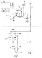
- An image sensor of the type mentioned can, for example, as in Fig. 1 can be constructed shown in the representative only a single pixel 11 is shown.
- the illustrated pixel 11 comprises a photosensitive detector element in the form of a so-called pinned diode (PD) 15, which is charge-coupled via a transfer gate 39 to a read-out node 41, which is designed as a so-called floating diffusion (FD).
- the readout node 41 is connected to the gate of a source follower converter field effect transistor (FET) 43, which is a charge-to-voltage converter circuit.
- FET field effect transistor
- the readout node 41 is connected to a positive power supply 51 via a reset FET 45.
- One of the two channel terminals of the converter FET 43 is also connected to the positive supply 51, whereas the other of the two channel terminals of the converter FET 43 can be connected to the column line 17 associated with the illustrated pixel via a selection FET 47 which acts as a row selection switch is.
- the column line 17 is intended to connect the pixels arranged in the associated column, in particular pixel 11, to a common column amplifier circuit 113.
- the column amplifier circuit 113 comprises a first capacitor 127, which is connected to one terminal to ground and to the other terminal via a Switch 149E is selectively connectable to the column line 17.
- the column amplifier circuit 113 further comprises a second capacitor 133, which is also connected to ground with one terminal and also connectable to the other terminal via a further switch 149D also optionally with the column line 17.
- the column amplifier circuit 113 comprises an amplifier 131, to whose negative input 137 the voltage applied to the first capacitor 127 voltage and at its positive input 135, the voltage applied to the second capacitor 133 voltage is input.
- the transfer gate 39 is connected via a control line TRF, the reset FET 45 is via a control line RES, the select FET 47 is connected via a control line SEL, the switch 149E is via a control line S 1 and the switch 149D is via a control line S2 controllable by a common control device 153 of the image sensor.
- the incident light during an exposure process is converted into electrical charge by the pinned diode 15, so that the pinned diode 15 fills with electrons.
- the control lines TRF, RES and SEL are each held at 0V, i. the thus controlled switches 39, 45, 47 are open.
- a voltage of 3.3 V is briefly applied to the control line RES in order to remove charge formed by leakage currents and / or scattered light from the readout node 41.
- a voltage of 3.3V is applied to the control line SEL (closing of the switch 47), and the switch 149E is closed.
- the voltage level of the readout node 41 is switched to the column line 17 via the converter FET 43 and the selection FET 47, and thus to the capacitor 127.
- the capacitor 127 is disconnected from the pixel 11 by opening the switch 149E.
- a voltage of 3.3V is briefly applied, so that the electrons can flow from the pinned diode 15 to the readout node 41.
- a fourth step (reading the signal)
- the switch 149D is closed.
- the voltage level of the readout node 41 is switched to the column line 17 via the converter FET 43 and the selection FET 47, and thus led to the capacitor 133.
- the capacitor 133 is disconnected from the pixel 11 again by opening the switch 149D, and the control line SEL is reset to 0V.
- a voltage of 3.3V is applied to remove the charge from the readout node 41 and any residual charges from the pinned diode 15 so that the next exposure process again with a can start completely "empty" pixels.
- Fig. 1 It is necessary that the charges produced by the incident light in the pinned diode 15 at the gate of the converter FET 43 cause a high voltage. This is achieved by keeping the capacity of the readout node 41 small. For example, with a capacitance of 2fF, each electron will cause a voltage change of 80 ⁇ V. If the camera has a noise level of, for example, 240 ⁇ V, then 3 electrons or 3 photons can already be detected.
- Fig. 1 Although described image sensor thus has a high photosensitivity, but only a small dynamic range. With the aforementioned capacitance of 2fF, the readout node 41 is already completely filled with 12000 electrons. 12,000 electrons cause a voltage of about 1V, which reaches the limit of the electrical range that can be passed to the outputs.
- the invention has for its object to provide a way to ensure a high dynamic range in an image sensor or a method of the type mentioned in addition to a high sensitivity to light.
- an image sensor having the features of claim 1, and in particular by the control device being designed such that the charge generated in a single exposure process in the respective detector element is transferred in multiple portions from the detector element to the readout node.
- this object is achieved by a method having the features of claim 17, and in particular by the fact that the charge generated during a single exposure operation in the respective detector element is transferred in a plurality of portions from the detector element to the readout node.
- the stepwise readout can increase the dynamics of the image sensor by a factor that corresponds to the number of charge transfers compared with the dynamics known from the prior art. If the charge generated in the detector element is read, for example, based on three charge transfers, the dynamics can be increased by a factor of three. If, for example, the read-out node has a saturation limit of 12,000 electrons and the detector element has a saturation limit of 36,000 electrons, a dynamics of 12,000: 1 is achieved for a noise level of three electrons. If the detector element has an even higher saturation limit, the dynamics can be characterized by a more than triply divided readout be further increased. In this case, since the capacity of the readout node may be made small (in proportion to the capacity of the detector element), high photosensitivity is maintained.
- Switchable capacitances for the pixels can thus be dispensed with in the case of the image sensor according to the invention and the method according to the invention. Although such switchable capacitances increase the dynamic range, they reduce the photosensitivity, since the space required by the respective capacitance, a respective additional transistor for the capacitance and an additional drive line is no longer available for the respective detector element. In addition, unwanted calibrations are required with such switchable capacitors.
- the charge is divided into a plurality of partial charges (or partial value measurement signals) which has been generated in the respective detector element due to a single exposure process, wherein, for example, a mechanical or an electronic shutter initiates or terminates the exposure process ,
- the image sensor is particularly suitable for recording moving subjects. Namely, the output signal of the image sensor is not generated from a plurality of partial value measuring signals corresponding to different exposure times, which could lead to a "smearing" of the image information.
- charge coupling is to be understood as meaning that a charge present in the detector element can be displaced into the readout node.
- the charge present in the readout node may in particular be a zero charge, ie after the reset by the reset device is then no more charge in the readout node available. This applies in particular to the reference value mentioned.
- the control device is designed in such a way that at least two successive transfer control signals are applied to the transfer gate in order to read out the charge generated in the respective detector element during a single exposure process, so that a respective charge transfer from the detector element to the readout node is enabled to generate by means of the converter circuit for each charge transfer, a separate partial value measurement signal which is proportional to the charge present in the readout node due to the respective charge transfer.
- the reset device is activated between the respective successive transfer control signals.
- the transfer control signals have different control values.
- the absolute value of the control value of the later of the two transfer control signals may be greater than the absolute value of the control value of the earlier of the two transfer control signals.
- the at least two transfer control signals may have different control voltage values. This means in particular that not every one of the control voltage values must correspond to the full operating voltage underlying the respective technology generation. As a result, the power consumption of the image sensor can be reduced.
- a transfer control signal whose magnitude control value is larger than the magnitude control value of another transfer control signal, the transfer of those charges which are not (yet) transferable by the other (smaller amount) transfer control signal is enabled. By grading the control values of the transfer control signals If the detector element is not saturated, it is also possible to generate partial value measuring signals which correspond to a zero charge.
- the detector element may comprise exactly two terminals, one terminal being coupled to a predetermined reference potential (e.g., ground) and the other terminal being coupled only to the transfer gate, i. the charge generated in the detector element can be transferred (via the transfer gate) directly to the readout node without a further switch or bias of the detector element.
- a predetermined reference potential e.g., ground
- the detector element may be formed as a photodiode, preferably as a pinned diode whose potential level is fixed.
- the readout node may be formed as a floating diffusion region whose potential level varies with the amount of charge present in the charge node.
- the pixels arranged in a respective column are connected, via a common column line, to a column amplifier circuit controllable by the control device, which comprises an amplifier and a number of subvalue signal memories corresponding to the number of successive transfer control signals, the control device being such is designed such that each of the partial value measuring signals corresponding to the charge transfer is transmitted to its own one of the partial value signal memories.
- the partial value measuring signals are preferably combined after their storage in the partial value signal memories and digitized together.
- the combined signal or total value measurement signal can then - because when reading all partial value signal memory to a common input of the relevant amplifier or A / D converter to be added (adding up the capacities of the partial value latch) - also be less than one or more of the partial value measuring signals.
- each of the partial value measurement signals it is also possible for each of the partial value measurement signals to be digitized individually first and stored as a digital value in the respective partial value signal memory, with the digital values subsequently being combined.
- the partial value signal stores can have identical capacities and / or be integrated.
- the respective column amplifier circuit comprises first switching means, wherein the partial value signal memories are connectable via the first switching means simultaneously with a first input of the amplifier.
- control device can be designed such that by means of the converter circuit, after activation of the reset device, a reference value measurement signal corresponding to the reference value of the charge is generated and transmitted to a reference value latch of the respective column amplifier circuit, the reference value latch having a second input of the amplifier connected or connectable.
- the reference value measurement signal corresponds to a defined charge in the readout node, in particular a zero charge.
- the reference value measuring signal can basically be generated before or after the generation of any of the partial value measuring signals.
- the respective column amplifier circuit comprises an additional amplifier and a residual signal latch, wherein the control device is designed such that one of the charge transfer corresponding partial value measurement signals is transmitted simultaneously to the associated partial value latch and the residual signal latch.
- the partial value measurement signal present in the residual value latch can then be compared with the total value measurement signal described above. Depending on the result of this comparison, the partial value measurement signal present in the residual value latch, the total value measurement signal or a combination of these two signals can be used to determine the charge generated in the detector element.
- the aforementioned at least one partial value measuring signal is, in particular, that measuring signal which corresponds to the last charge transfer. If it is determined that only charge was actually transferred from the detector element to the read-out node only in the last charge transfer, the partial value measurement signal stored in the residual value store alone can be used to determine the charge generated in the detector element, whereby the signal-to-noise ratio Ratio is improved over the use of the total value measurement signal described above.
- the respective residual value latch is connected or connectable to a first input of the additional amplifier and / or the reference value latch described above is connected or connectable to a second input of the additional amplifier.
- the additional amplifier (assigned to the residual value latch) has a higher amplification factor than the named amplifier (assigned to the partial value signal memories), wherein a suitably adapted transition can be provided in order to determine the charge generated in the detector element to use the partial value measurement signal present in the residual value latch, the total value measurement signal or a combination of these two signals.
- the signal path with the lower amplification factor (for the total value measurement signal) in this case allows the full modulation, while for the signal path with the higher amplification factor (for the signal of the remainder latch) with respect to the noise and the disturbances of all stages, after the relevant Gain provided an improved signal / noise ratio. Through a combination of these two channels thus an even higher dynamics is achieved.
- the respective column amplifier circuit includes second switch means.
- a separate switch is provided between the column line and each of the latches.
- the latches i. the divided-value latches, the above-described reference-value latches, and the residual-value latches are each formed as a capacitor.
- the image sensor is embodied such that the partial value measurement signals corresponding to the charge transfers of a single exposure process are individually digitized and the digitized partial value measurement signals are subsequently combined to form a digital total value measurement signal.
- the partial value measurement signals corresponding to the charge transfers of a single exposure process are individually digitized and the digitized partial value measurement signals are subsequently combined to form a digital total value measurement signal.
- each column should be provided with its own A / D converter or, for several or all columns, a common A / D converter.
- exactly one analog signal memory can be provided for each column, wherein the control device is designed such that each of the charge transfer corresponding partial value measurement signals or additionally at least one reference value measurement signal is transmitted to the analog signal memory to be digitized thereafter.
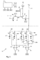
- the in Fig. 2 illustrated image sensor according to the invention comprises a pixel 11 and a column line 17, which is the in Fig. 1 the prior art described pixel 11 or the in Fig. 1 corresponds to column line 17 described in the prior art.
- the image sensor includes according to Fig. 2 an amplifier circuit 13 which outputs an amplifier 131 Fig.1 corresponding amplifier 31 (with a positive input 35 and a negative input 37), which is referred to as additional amplifier 31 hereinafter, a capacitor 133 from Fig. 1 corresponding residual capacitor 33, a capacitor 127 from Fig. 1 corresponding reference value capacitor 27, one of the switch 149E Fig. 1 corresponding switch 49E and one the switch 149D Fig. 1 corresponding switch 49D includes.
- the above components are interconnected in the same way as the corresponding components Fig. 1 , The preceding remarks to Fig. 1 are therefore part of the disclosure of the invention.
- the image sensor according to Fig. 2 further comprises three parallel to each other and each connected to ground part value capacitors 21A, 21B, 21C, which are identical and each with its own switch 49A, 49B, 49C, which are hereinafter referred to as the second switch 49A, 49B, 49C, with the column line 17 are connectable.
- each divider capacitor 21A, 21B, 21C is provided with a further switch 23A, 23B, 23C, the further switches 23A, 23B, 23C being referred to below as respective first switches 23A, 23B, 23C.
- the three divisional capacitors 21A, 21B, 21C are connected to one another via the first switches 23A, 23B, 23C and at the same time to the positive input 25 of an amplifier 19.
- the negative input 29 of the amplifier 19 is connected to the reference value capacitor 27.
- one of the control device 153 from Fig.1 corresponding control device 53 in addition to the already Fig. 1 also controls the first switches 23A, 23B, 23C and the second switches 49A, 49B, 49C (via the control lines S3, S4, S5, S6, S7, S8).
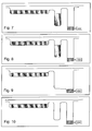
- Fig. 3 shows a semiconductor substrate in which the pinned diode 15 is provided, which is charge coupled via a transfer gate 39 with the trained as a "floating diffusion" readout node 41. Via the reset FET 45, the readout node 41 is connectable to a diffused channel terminal to which the positive supply 51 is applied.
- the pinned diode 15 or its potential well is filled with charge, as in Fig. 4 (after exposure, immediately before reading) is shown.
- the Readout node 41 or its potential well also contains a small amount of charge that was generated by leakage currents and / or stray light.
- a voltage of 3.3V is first applied to the control line RES. This can, as in Fig. 5 (Reset 1) is shown, the charge generated in the pinned diode 15 from the readout node 41 to the positive supply voltage 51 flow.
- the control line RES is then reset to 0V ( Fig. 6 , End reset 1). This ensures that the readout node 41 does not already contain charge prior to a first charge transfer, as described below.
- Fig. 7 (Transfer 1) is then applied by means of a first transfer control signal to the control line TRF a mean voltage of 2.5V, so that a first part of the charge generated in the pinned diode 15 can flow into the readout node 41. Subsequently, the control line TRF is again set to 0V, so that the readout node 41 now contains the first part of the charge ( Fig. 8 , End transfer 1).
- control line SEL is set to a voltage of 3.3V and the second switch 49A is closed.
- the voltage level generated by the charge in the readout node 41 via the converter FET 43 is switched to the column line 17 via the select FET 47 and thus fed to the divisor capacitor 21A (read signal 1).
- the divisional capacitor 21A is again disconnected from the pixel 11 by opening the second switch 49A, so that in the partial value capacitor 21A, in the form of a corresponding charge, an analog first divisional voltage signal is stored after the first charge transfer in the readout node 41 present charge is proportional.
- control line RES is set to a voltage of 3.3V, so that the charge can flow out of the readout node 41 to the positive supply 51 ( Fig. 9 , Reset 2).
- the control line RES is then reset to 0V ( Fig. 10 , End reset 2). This in turn ensures that the readout node 41 does not already contain charge prior to a second charge transfer as described below.
- Fig. 11 (Transfer 2) is applied by means of a second transfer control signal, the control line TRF to a slightly higher voltage of 2.8V, so that a second part of the charge generated in the pinned diode 15 can flow into the readout node 41. Subsequently, the control line TRF is again set to 0V, so that the read-out node 41 now contains the second part of the charge ( Fig. 12 , End transfer 2).
- the second switch 49B is closed. Thereby, the voltage level of the readout node 41 caused by the second charge transfer is conducted via the converter FET 43 and the select FET 47 to the column line 17 and thus to the divisor capacitor 21B (read signal 2).
- the capacitor 21B is again disconnected from the pixel 11 by opening the second switch 49B, so that an analog second divisional voltage signal is stored in the divisional capacitor 21B, that after the second charge transfer in the readout node 41 existing charge is proportional.
- control line RES is set to a voltage of 3.3V, so that the charge can flow from the readout node 41 to the positive supply 51 ( Fig. 13 , Reset 3).
- the control line RES is then reset to 0V ( Fig. 14 , End reset 2). This will ensure the readout node 41 does not already contain charge prior to the generation of a reference voltage signal, as will be described below.
- the second switch 49E is closed. Thereby, the voltage level of the readout node 41 is switched to the column line 17 via the converter FET 43 and the select FET 47, and thus to the reference value capacitor 27 (read reference). After the system is settled, the reference value capacitor 27 is disconnected from the pixel 11 by opening the second switch 49E.
- control line TRF is set to the full voltage of 3.3V by means of a third transfer control signal.
- the control line TRF is again set to 0V, so that the read-out node 41 now contains the third part of the charge ( Fig. 16 , End transfer 3).
- the second switches 49C, 49D are then closed. Thereby, the voltage level of the readout node 41 caused by the third charge transfer is switched to the column line 17 via the converter FET 43 and the select FET 47, and thus led to both the fractional value capacitor 21C and the residual value capacitor 33.
- the divisional capacitor 21C and the residual capacitor 33 are separated again from the pixel 11 by opening the second switches 49C, 49D, so that in the divisional capacitor 21C and the residual capacitor in each case an analog third partial value voltage signal is stored which is proportional to the charge present in the read-out node 41 after the third charge transfer.
- control line SEL is reset to 0V.
- the control lines RES and TRF are connected to a voltage of 3.3V ( Fig. 17 , Reset 4). This will remove the charge in the readout node 41 (and any residual charges present in the pinned diode 15). Then the control lines RES and TRF are reset to 0V ( Fig. 18 , End reset 4). The pixel is "empty" and the next exposure process can begin.
- the voltages LOW and HIGH, which are now applied to the amplifiers 19, 31, are fed to a common A / D converter or to separate A / D converters and digitized.
- the reference value voltage signal i. of the voltage signal of the empty readout node 41, the total value voltage signal (at the amplifier 19) and the sub-value voltage signal of the third charge transfer (at the additional amplifier 31)
- the voltage values of the transfer control signals are adapted to the depth of the potential well of the pinned diode 15.
- the first both read operations do not transfer charges from the pinned diode 15 to the readout node 41.
- the two divisional capacitors 21A, 21B thus each contain the divisional voltage signal of the "empty" readout node 41, i. the reference value voltage signal which is also stored in the reference value capacitor 27.
- the voltage HIGH at the output of the amplifier 19 is therefore exactly a fraction equal to one third of the voltage LOW at the output of the additional amplifier 31. In this case, the voltage LOW is used to determine the charge generated in the pinned diode 15 and HIGH ignored.
- the aforementioned fraction (here: one-third) is precisely known without calibrating the column amplifier circuit 13, since due to the integrated design of the capacitors 21A, 21B, 21C and 33 they can be provided with identical respective capacitance.
- the pinned diode 15 If the pinned diode 15 is filled more than the above-mentioned level, charges are transmitted from the pinned diode 15 to the readout node 41 in at least two, in particular the three read operations.
- the capacitors 21B, 21C and 21A, 21B, 21C thus contain the corresponding divisional voltage signals of the respective filled readout node 41.
- the voltage LOW at the output of the additional amplifier 31 is invalid in this case and is ignored because it does not cover the entire in the Pinned diode 15 represents generated charge. For determination Consequently, only the voltage HIGH is used in this case in the case of the charge generated in the pinned diode 15.
- either the signal HIGH or the signal LOW is selected for each pixel 11 taking into account the ratio of the total capacitance of the capacitors 21A, 21B and 21C to the capacitance of the capacitor 33 (signal HIGH corresponds to one third of the signal LOW for identical capacitances).
- both signals may also be considered, i. with each other (e.g., for a charge of 10,000 to 12,000 electrons in the pinned diode 15).
- the signals selected for the individual pixels 11 are finally assembled into a common image.
- the dynamic range of the image sensor with respect to an image sensor that provides only the signal LOW can be increased.
- This increases the linear dynamics.
- the two amplifiers 19, 31 with the different amplification factors are arranged at the beginning of the signal path, ie the different amplification of the relevant partial value measuring signals takes place very early in the signal processing path.
- the billing of the two signals takes place with each other as late as possible in the signal processing path, and there are separate A / D converter are provided.
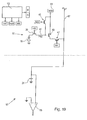
- Fig. 19 shows a further embodiment of the invention with respect to the embodiment according to Fig. 2 simplified column amplifier circuit 13.
- the reading of the pinned diode 15 is basically analogous as in connection with Fig. 3 to 18 That is, the charge generated in a pinned diode 15 during a single exposure process is transferred in multiple portions to the readout node 41.
- the image sensor according to Fig. 19 it is designed in such a way that the partial value measurement signals corresponding to the charge transfer of a single exposure process are individually digitized and the digitized partial value measurement signals are subsequently combined to form a digital total value measurement signal.
- only a single analog signal memory 21 is used, in which the partial value measurement signals and the reference value measurement signal are sequentially stored before each digitized by an A / D converter, not shown, which is connected downstream of the amplifier 19 ,
- the signal memory 21 can also be omitted if the respective measurement signal is digitized directly.
Landscapes
- Engineering & Computer Science (AREA)
- Multimedia (AREA)
- Signal Processing (AREA)
- Physics & Mathematics (AREA)
- Nonlinear Science (AREA)
- Transforming Light Signals Into Electric Signals (AREA)
- Solid State Image Pick-Up Elements (AREA)
Applications Claiming Priority (1)
| Application Number | Priority Date | Filing Date | Title |
|---|---|---|---|
| DE102007045448.3A DE102007045448B4 (de) | 2007-09-24 | 2007-09-24 | Bildsensor |
Publications (3)
| Publication Number | Publication Date |
|---|---|
| EP2040458A2 true EP2040458A2 (fr) | 2009-03-25 |
| EP2040458A3 EP2040458A3 (fr) | 2012-10-17 |
| EP2040458B1 EP2040458B1 (fr) | 2018-11-07 |
Family
ID=40120101
Family Applications (1)
| Application Number | Title | Priority Date | Filing Date |
|---|---|---|---|
| EP08016805.7A Active EP2040458B1 (fr) | 2007-09-24 | 2008-09-24 | Capteur d'images |
Country Status (3)
| Country | Link |
|---|---|
| US (1) | US7952629B2 (fr) |
| EP (1) | EP2040458B1 (fr) |
| DE (1) | DE102007045448B4 (fr) |
Cited By (3)
| Publication number | Priority date | Publication date | Assignee | Title |
|---|---|---|---|---|
| EP2369834A3 (fr) * | 2009-11-13 | 2012-05-30 | Arnold & Richter Cine Technik GmbH & Co. Betriebs KG | Capteur d'image |
| EP2424230A3 (fr) * | 2010-08-30 | 2012-10-24 | Arnold & Richter Cine Technik GmbH & Co. Betriebs KG | Capteur d'image et procédé de lecture d'un capteur d'image |
| EP2456194A3 (fr) * | 2010-11-19 | 2013-02-13 | Arnold&Richter Cine Technik GmbH&Co. Betriebs KG | Capteur d'images |
Families Citing this family (17)
| Publication number | Priority date | Publication date | Assignee | Title |
|---|---|---|---|---|
| JP5055469B2 (ja) * | 2006-08-04 | 2012-10-24 | 新世代株式会社 | イメージセンサ及びイメージセンサシステム |
| US8233070B2 (en) * | 2009-03-27 | 2012-07-31 | International Business Machines Corporation | Variable dynamic range pixel sensor cell, design structure and method |
| GB201012631D0 (en) * | 2010-07-28 | 2010-09-15 | Isis Innovation | Image sensor and method of sensing |
| DE102010051440A1 (de) * | 2010-11-15 | 2012-05-16 | Arnold & Richter Cine Technik Gmbh & Co. Betriebs Kg | Bildsensor |
| DE102010051438B4 (de) * | 2010-11-15 | 2024-03-14 | Arnold & Richter Cine Technik Gmbh & Co. Betriebs Kg | Bildsensor |
| DE102011004578A1 (de) | 2011-02-23 | 2012-08-23 | Robert Bosch Gmbh | Kameraanordnung sowie Verfahren zum Betreiben |
| DE102011101835A1 (de) | 2011-05-16 | 2012-11-22 | Arnold & Richter Cine Technik Gmbh & Co. Betriebs Kg | Bildsensor |
| US8569806B2 (en) | 2011-09-02 | 2013-10-29 | Hoon Kim | Unit pixel of image sensor and photo detector thereof |
| US8610234B2 (en) | 2011-09-02 | 2013-12-17 | Hoon Kim | Unit pixel of image sensor and photo detector thereof |
| DE102011120099B4 (de) | 2011-12-02 | 2024-05-29 | Arnold & Richter Cine Technik Gmbh & Co. Betriebs Kg | Bildsensor und Verfahren zum Auslesen eines Bildsensors |
| JP6192390B2 (ja) * | 2013-07-05 | 2017-09-06 | キヤノン株式会社 | 光電変換装置、光電変換システム |
| DE102013209164B4 (de) | 2013-05-17 | 2023-01-19 | Arnold & Richter Cine Technik Gmbh & Co. Betriebs Kg | Digitale Filmkamera |
| JP6188433B2 (ja) * | 2013-06-07 | 2017-08-30 | 浜松ホトニクス株式会社 | 固体撮像装置 |
| JP6370044B2 (ja) * | 2013-12-25 | 2018-08-08 | キヤノン株式会社 | 撮像装置、撮像システム、撮像装置の駆動方法 |
| US9735188B2 (en) | 2015-01-15 | 2017-08-15 | Hoon Kim | Image sensor with solar cell function |
| US9743027B2 (en) * | 2015-06-24 | 2017-08-22 | Semiconductor Components Industries, Llc | Image sensor with high dynamic range and method |
| US12289549B2 (en) | 2022-11-09 | 2025-04-29 | Fairchild Imaging, Inc | Image sensor with charge transfer between pixels |
Family Cites Families (38)
| Publication number | Priority date | Publication date | Assignee | Title |
|---|---|---|---|---|
| US3983395A (en) | 1974-11-29 | 1976-09-28 | General Electric Company | MIS structures for background rejection in infrared imaging devices |
| JPH01251756A (ja) | 1988-03-31 | 1989-10-06 | Toshiba Corp | 電荷結合装置 |
| JPH02122668A (ja) | 1988-11-01 | 1990-05-10 | Nec Corp | 固体撮像装置 |
| JP2641802B2 (ja) | 1990-12-27 | 1997-08-20 | 富士通株式会社 | 撮像装置 |
| US5309243A (en) | 1992-06-10 | 1994-05-03 | Eastman Kodak Company | Method and apparatus for extending the dynamic range of an electronic imaging system |
| JPH07327130A (ja) | 1994-06-01 | 1995-12-12 | Fuji Photo Film Co Ltd | 画像読取装置 |
| DE69628187D1 (de) | 1995-11-07 | 2003-06-18 | California Inst Of Techn | Bildsensor mit linearem ausgang mit grossem dynamikbereich |
| EP0903935A1 (fr) | 1997-09-22 | 1999-03-24 | Interuniversitair Micro-Elektronica Centrum Vzw | Méthode pour obtenir un signal de lecture d'une structure de pixel basée sur le CMOS et une telle structure de pixel basée sur le CMOS |
| US6078037A (en) | 1998-04-16 | 2000-06-20 | Intel Corporation | Active pixel CMOS sensor with multiple storage capacitors |
| KR100291179B1 (ko) | 1998-06-29 | 2001-07-12 | 박종섭 | 자기정렬된실리사이드층을갖는씨모스이미지센서및그제조방법 |
| US6133862A (en) | 1998-07-31 | 2000-10-17 | Intel Corporation | Method and apparatus to reduce row reset noise in photodiode |
| KR100297714B1 (ko) | 1998-09-01 | 2001-08-07 | 윤종용 | 넓은동적범위를갖는영상장치및이의영상신호처리방법 |
| US6850278B1 (en) | 1998-11-27 | 2005-02-01 | Canon Kabushiki Kaisha | Solid-state image pickup apparatus |
| DE19907971A1 (de) | 1999-02-24 | 2000-08-31 | Bosch Gmbh Robert | Bildsensor und Verfahren zum Betreiben eines Bildsensors |
| WO2000078034A2 (fr) * | 1999-06-15 | 2000-12-21 | Photobit Corporation | Capteur d'image a double sensibilite |
| JP3667220B2 (ja) | 1999-10-05 | 2005-07-06 | キヤノン株式会社 | 固体撮像装置、撮像システム及び固体撮像装置の駆動方法 |
| US7324144B1 (en) * | 1999-10-05 | 2008-01-29 | Canon Kabushiki Kaisha | Solid image pickup device, image pickup system and method of driving solid image pickup device |
| US6710804B1 (en) | 2000-01-18 | 2004-03-23 | Eastman Kodak Company | CMOS active pixel image sensor with extended dynamic range and sensitivity |
| JP3558589B2 (ja) | 2000-06-14 | 2004-08-25 | Necエレクトロニクス株式会社 | Mos型イメージセンサ及びその駆動方法 |
| US6580106B2 (en) | 2001-01-12 | 2003-06-17 | Isetex. Inc | CMOS image sensor with complete pixel reset without kTC noise generation |
| JP4154157B2 (ja) | 2002-02-25 | 2008-09-24 | 株式会社東芝 | 撮像装置 |
| JP2003319250A (ja) | 2002-04-22 | 2003-11-07 | Toshiba Lsi System Support Kk | 撮像装置および撮像方法 |
| JP2004229257A (ja) | 2003-01-22 | 2004-08-12 | Honda Motor Co Ltd | イメージセンサ |
| JP2004254151A (ja) | 2003-02-21 | 2004-09-09 | Fuji Film Microdevices Co Ltd | 撮像装置及び撮像方法 |
| US20050083421A1 (en) * | 2003-10-16 | 2005-04-21 | Vladimir Berezin | Dynamic range enlargement in CMOS image sensors |
| JP4421353B2 (ja) | 2004-04-01 | 2010-02-24 | 浜松ホトニクス株式会社 | 固体撮像装置 |
| JP4416668B2 (ja) | 2005-01-14 | 2010-02-17 | キヤノン株式会社 | 固体撮像装置、その制御方法及びカメラ |
| JP4459064B2 (ja) * | 2005-01-14 | 2010-04-28 | キヤノン株式会社 | 固体撮像装置、その制御方法及びカメラ |
| EP1689164B1 (fr) | 2005-02-03 | 2007-12-19 | Sony Ericsson Mobile Communications AB | Procédé et appareil de création d'images améliorées à l'aide de plusieurs expositions consécutives |
| US7616256B2 (en) | 2005-03-21 | 2009-11-10 | Dolby Laboratories Licensing Corporation | Multiple exposure methods and apparatus for electronic cameras |
| CA2511220C (fr) | 2005-03-21 | 2012-08-14 | Sunnybrook Technologies Inc. | Methodes et appareil d'exposition multiple pour appareils photos electroniques |
| US7541628B2 (en) | 2005-07-09 | 2009-06-02 | Samsung Electronics Co., Ltd. | Image sensors including active pixel sensor arrays |
| US20090040364A1 (en) | 2005-08-08 | 2009-02-12 | Joseph Rubner | Adaptive Exposure Control |
| US7829832B2 (en) | 2005-08-30 | 2010-11-09 | Aptina Imaging Corporation | Method for operating a pixel cell using multiple pulses to a transistor transfer gate |
| EP1929769A1 (fr) | 2005-09-19 | 2008-06-11 | Robert Bosch Gmbh | Appareil de prise de vues |
| JP4862473B2 (ja) * | 2005-10-28 | 2012-01-25 | ソニー株式会社 | 固体撮像装置、固体撮像装置の駆動方法および撮像装置 |
| KR100737916B1 (ko) | 2005-12-19 | 2007-07-10 | 삼성전자주식회사 | 이미지 센서 그리고 그것을 위한 테스트 시스템 및 테스트방법 |
| US7667183B2 (en) | 2006-03-10 | 2010-02-23 | Samsung Electronics Co., Ltd. | Image sensor with high fill factor pixels and method for forming an image sensor |
-
2007
- 2007-09-24 DE DE102007045448.3A patent/DE102007045448B4/de active Active
-
2008
- 2008-09-23 US US12/235,808 patent/US7952629B2/en active Active
- 2008-09-24 EP EP08016805.7A patent/EP2040458B1/fr active Active
Non-Patent Citations (1)
| Title |
|---|
| None |
Cited By (4)
| Publication number | Priority date | Publication date | Assignee | Title |
|---|---|---|---|---|
| EP2369834A3 (fr) * | 2009-11-13 | 2012-05-30 | Arnold & Richter Cine Technik GmbH & Co. Betriebs KG | Capteur d'image |
| US8582010B2 (en) | 2009-11-13 | 2013-11-12 | Arnold & Richter Cine Technik Gmbh & Co. Betriebs Kg | Image sensor |
| EP2424230A3 (fr) * | 2010-08-30 | 2012-10-24 | Arnold & Richter Cine Technik GmbH & Co. Betriebs KG | Capteur d'image et procédé de lecture d'un capteur d'image |
| EP2456194A3 (fr) * | 2010-11-19 | 2013-02-13 | Arnold&Richter Cine Technik GmbH&Co. Betriebs KG | Capteur d'images |
Also Published As
| Publication number | Publication date |
|---|---|
| US7952629B2 (en) | 2011-05-31 |
| DE102007045448B4 (de) | 2025-01-30 |
| EP2040458B1 (fr) | 2018-11-07 |
| DE102007045448A1 (de) | 2009-04-02 |
| US20100073538A1 (en) | 2010-03-25 |
| EP2040458A3 (fr) | 2012-10-17 |
Similar Documents
| Publication | Publication Date | Title |
|---|---|---|
| EP2040458B1 (fr) | Capteur d'images | |
| DE69606147T2 (de) | Schaltung, Bildelement, Vorrichtung und Verfahren zur Verminderung des Rauschens örtlich unveränderlicher Muster in Festkörperbildaufnahmevorrichtungen | |
| DE102009053281B4 (de) | Bildsensor | |
| DE69831071T2 (de) | Cmos bildsensor mit verbessertem füllfaktor | |
| DE60030802T2 (de) | Bildsensor mit Messsung der Sättigungszeitmessung zur Erweiterung des Dynamikbereichs | |
| EP0878091B1 (fr) | Capteur d'image couleur pour exposition de courte duree | |
| DE60105393T2 (de) | X-Y-Adressen-Festkörperbildaufnehmer | |
| AT505513B1 (de) | Bildsensor, verfahren zum betreiben eines bildsensors und computerprogramm | |
| DE112022002176T5 (de) | Pixelanordnung, Bildsensor und Verfahren zum Betrieb einer Pixelanordnung | |
| DE60030959T2 (de) | Photodetektorvorrichtung | |
| DE102011120099B4 (de) | Bildsensor und Verfahren zum Auslesen eines Bildsensors | |
| DE69935895T2 (de) | Architektur eines aktiven pixelsensors mit drei transistoren und korrelierter doppelabtastung | |
| DE2912884A1 (de) | Photomessfuehlereinrichtung und diese verwendendes bildabtastsystem | |
| DE102010035811B4 (de) | Bildsensor und Verfahren zum Auslesen eines Bildsensors | |
| DE102010051986B4 (de) | Bildsensor | |
| WO2004040904A1 (fr) | Capteur optoelectronique | |
| DE69910838T2 (de) | Reduzierung von streifenförmigen Störungen in CMOS Bildsensoren | |
| DE10065887A1 (de) | Photosensorschaltung | |
| DE19533061C2 (de) | Photoelektrische Halbleiter-Lichterfassungseinrichtung mit programmierbarem Offset-Strom und Bildsensor mit einer solchen Einrichtung | |
| DE102009019034A1 (de) | Bildsensor | |
| EP4175312B1 (fr) | Capteur d'image | |
| EP3985965B1 (fr) | Convertisseur d'image | |
| DE102021108693B4 (de) | Vorrichtung und Verfahren zur Ermittlung von mindestens zwei referenzwertbezogenen Pixel-Signalwerten eines oder mehrerer LOFIC Pixel per korrelierter Doppelabtastung | |
| EP0934649A1 (fr) | Procede de detection d'un signal d'image | |
| DE102020111562A1 (de) | Bildsensor |
Legal Events
| Date | Code | Title | Description |
|---|---|---|---|
| PUAI | Public reference made under article 153(3) epc to a published international application that has entered the european phase |
Free format text: ORIGINAL CODE: 0009012 |
|
| AK | Designated contracting states |
Kind code of ref document: A2 Designated state(s): AT BE BG CH CY CZ DE DK EE ES FI FR GB GR HR HU IE IS IT LI LT LU LV MC MT NL NO PL PT RO SE SI SK TR |
|
| AX | Request for extension of the european patent |
Extension state: AL BA MK RS |
|
| PUAL | Search report despatched |
Free format text: ORIGINAL CODE: 0009013 |
|
| AK | Designated contracting states |
Kind code of ref document: A3 Designated state(s): AT BE BG CH CY CZ DE DK EE ES FI FR GB GR HR HU IE IS IT LI LT LU LV MC MT NL NO PL PT RO SE SI SK TR |
|
| AX | Request for extension of the european patent |
Extension state: AL BA MK RS |
|
| RIC1 | Information provided on ipc code assigned before grant |
Ipc: H04N 5/374 20110101ALI20120910BHEP Ipc: H04N 5/355 20110101AFI20120910BHEP |
|
| 17P | Request for examination filed |
Effective date: 20130417 |
|
| AKX | Designation fees paid |
Designated state(s): AT BE BG CH CY CZ DE DK EE ES FI FR GB GR HR HU IE IS IT LI LT LU LV MC MT NL NO PL PT RO SE SI SK TR |
|
| 17Q | First examination report despatched |
Effective date: 20140317 |
|
| STAA | Information on the status of an ep patent application or granted ep patent |
Free format text: STATUS: EXAMINATION IS IN PROGRESS |
|
| REG | Reference to a national code |
Ref country code: DE Ref legal event code: R079 Ref document number: 502008016436 Country of ref document: DE Free format text: PREVIOUS MAIN CLASS: H04N0003150000 Ipc: H04N0005355000 |
|
| GRAP | Despatch of communication of intention to grant a patent |
Free format text: ORIGINAL CODE: EPIDOSNIGR1 |
|
| STAA | Information on the status of an ep patent application or granted ep patent |
Free format text: STATUS: GRANT OF PATENT IS INTENDED |
|
| INTG | Intention to grant announced |
Effective date: 20180409 |
|
| RIC1 | Information provided on ipc code assigned before grant |
Ipc: H04N 5/378 20110101ALI20180323BHEP Ipc: H04N 5/3745 20110101ALI20180323BHEP Ipc: H04N 5/355 20110101AFI20180323BHEP |
|
| GRAS | Grant fee paid |
Free format text: ORIGINAL CODE: EPIDOSNIGR3 |
|
| GRAA | (expected) grant |
Free format text: ORIGINAL CODE: 0009210 |
|
| STAA | Information on the status of an ep patent application or granted ep patent |
Free format text: STATUS: THE PATENT HAS BEEN GRANTED |
|
| AK | Designated contracting states |
Kind code of ref document: B1 Designated state(s): AT BE BG CH CY CZ DE DK EE ES FI FR GB GR HR HU IE IS IT LI LT LU LV MC MT NL NO PL PT RO SE SI SK TR |
|
| REG | Reference to a national code |
Ref country code: GB Ref legal event code: FG4D Free format text: NOT ENGLISH |
|
| REG | Reference to a national code |
Ref country code: CH Ref legal event code: EP Ref country code: AT Ref legal event code: REF Ref document number: 1063496 Country of ref document: AT Kind code of ref document: T Effective date: 20181115 |
|
| REG | Reference to a national code |
Ref country code: IE Ref legal event code: FG4D Free format text: LANGUAGE OF EP DOCUMENT: GERMAN |
|
| REG | Reference to a national code |
Ref country code: DE Ref legal event code: R096 Ref document number: 502008016436 Country of ref document: DE |
|
| REG | Reference to a national code |
Ref country code: NL Ref legal event code: FP |
|
| REG | Reference to a national code |
Ref country code: LT Ref legal event code: MG4D |
|
| PG25 | Lapsed in a contracting state [announced via postgrant information from national office to epo] |
Ref country code: HR Free format text: LAPSE BECAUSE OF FAILURE TO SUBMIT A TRANSLATION OF THE DESCRIPTION OR TO PAY THE FEE WITHIN THE PRESCRIBED TIME-LIMIT Effective date: 20181107 Ref country code: ES Free format text: LAPSE BECAUSE OF FAILURE TO SUBMIT A TRANSLATION OF THE DESCRIPTION OR TO PAY THE FEE WITHIN THE PRESCRIBED TIME-LIMIT Effective date: 20181107 Ref country code: LT Free format text: LAPSE BECAUSE OF FAILURE TO SUBMIT A TRANSLATION OF THE DESCRIPTION OR TO PAY THE FEE WITHIN THE PRESCRIBED TIME-LIMIT Effective date: 20181107 Ref country code: IS Free format text: LAPSE BECAUSE OF FAILURE TO SUBMIT A TRANSLATION OF THE DESCRIPTION OR TO PAY THE FEE WITHIN THE PRESCRIBED TIME-LIMIT Effective date: 20190307 Ref country code: NO Free format text: LAPSE BECAUSE OF FAILURE TO SUBMIT A TRANSLATION OF THE DESCRIPTION OR TO PAY THE FEE WITHIN THE PRESCRIBED TIME-LIMIT Effective date: 20190207 Ref country code: FI Free format text: LAPSE BECAUSE OF FAILURE TO SUBMIT A TRANSLATION OF THE DESCRIPTION OR TO PAY THE FEE WITHIN THE PRESCRIBED TIME-LIMIT Effective date: 20181107 Ref country code: BG Free format text: LAPSE BECAUSE OF FAILURE TO SUBMIT A TRANSLATION OF THE DESCRIPTION OR TO PAY THE FEE WITHIN THE PRESCRIBED TIME-LIMIT Effective date: 20190207 Ref country code: LV Free format text: LAPSE BECAUSE OF FAILURE TO SUBMIT A TRANSLATION OF THE DESCRIPTION OR TO PAY THE FEE WITHIN THE PRESCRIBED TIME-LIMIT Effective date: 20181107 |
|
| PG25 | Lapsed in a contracting state [announced via postgrant information from national office to epo] |
Ref country code: SE Free format text: LAPSE BECAUSE OF FAILURE TO SUBMIT A TRANSLATION OF THE DESCRIPTION OR TO PAY THE FEE WITHIN THE PRESCRIBED TIME-LIMIT Effective date: 20181107 Ref country code: PT Free format text: LAPSE BECAUSE OF FAILURE TO SUBMIT A TRANSLATION OF THE DESCRIPTION OR TO PAY THE FEE WITHIN THE PRESCRIBED TIME-LIMIT Effective date: 20190307 Ref country code: GR Free format text: LAPSE BECAUSE OF FAILURE TO SUBMIT A TRANSLATION OF THE DESCRIPTION OR TO PAY THE FEE WITHIN THE PRESCRIBED TIME-LIMIT Effective date: 20190208 |
|
| PG25 | Lapsed in a contracting state [announced via postgrant information from national office to epo] |
Ref country code: DK Free format text: LAPSE BECAUSE OF FAILURE TO SUBMIT A TRANSLATION OF THE DESCRIPTION OR TO PAY THE FEE WITHIN THE PRESCRIBED TIME-LIMIT Effective date: 20181107 Ref country code: PL Free format text: LAPSE BECAUSE OF FAILURE TO SUBMIT A TRANSLATION OF THE DESCRIPTION OR TO PAY THE FEE WITHIN THE PRESCRIBED TIME-LIMIT Effective date: 20181107 Ref country code: CZ Free format text: LAPSE BECAUSE OF FAILURE TO SUBMIT A TRANSLATION OF THE DESCRIPTION OR TO PAY THE FEE WITHIN THE PRESCRIBED TIME-LIMIT Effective date: 20181107 Ref country code: IT Free format text: LAPSE BECAUSE OF FAILURE TO SUBMIT A TRANSLATION OF THE DESCRIPTION OR TO PAY THE FEE WITHIN THE PRESCRIBED TIME-LIMIT Effective date: 20181107 |
|
| REG | Reference to a national code |
Ref country code: DE Ref legal event code: R097 Ref document number: 502008016436 Country of ref document: DE |
|
| PG25 | Lapsed in a contracting state [announced via postgrant information from national office to epo] |
Ref country code: RO Free format text: LAPSE BECAUSE OF FAILURE TO SUBMIT A TRANSLATION OF THE DESCRIPTION OR TO PAY THE FEE WITHIN THE PRESCRIBED TIME-LIMIT Effective date: 20181107 Ref country code: EE Free format text: LAPSE BECAUSE OF FAILURE TO SUBMIT A TRANSLATION OF THE DESCRIPTION OR TO PAY THE FEE WITHIN THE PRESCRIBED TIME-LIMIT Effective date: 20181107 Ref country code: SK Free format text: LAPSE BECAUSE OF FAILURE TO SUBMIT A TRANSLATION OF THE DESCRIPTION OR TO PAY THE FEE WITHIN THE PRESCRIBED TIME-LIMIT Effective date: 20181107 |
|
| PLBE | No opposition filed within time limit |
Free format text: ORIGINAL CODE: 0009261 |
|
| STAA | Information on the status of an ep patent application or granted ep patent |
Free format text: STATUS: NO OPPOSITION FILED WITHIN TIME LIMIT |
|
| 26N | No opposition filed |
Effective date: 20190808 |
|
| PG25 | Lapsed in a contracting state [announced via postgrant information from national office to epo] |
Ref country code: SI Free format text: LAPSE BECAUSE OF FAILURE TO SUBMIT A TRANSLATION OF THE DESCRIPTION OR TO PAY THE FEE WITHIN THE PRESCRIBED TIME-LIMIT Effective date: 20181107 |
|
| PG25 | Lapsed in a contracting state [announced via postgrant information from national office to epo] |
Ref country code: TR Free format text: LAPSE BECAUSE OF FAILURE TO SUBMIT A TRANSLATION OF THE DESCRIPTION OR TO PAY THE FEE WITHIN THE PRESCRIBED TIME-LIMIT Effective date: 20181107 |
|
| PG25 | Lapsed in a contracting state [announced via postgrant information from national office to epo] |
Ref country code: MC Free format text: LAPSE BECAUSE OF FAILURE TO SUBMIT A TRANSLATION OF THE DESCRIPTION OR TO PAY THE FEE WITHIN THE PRESCRIBED TIME-LIMIT Effective date: 20181107 |
|
| REG | Reference to a national code |
Ref country code: CH Ref legal event code: PL |
|
| PG25 | Lapsed in a contracting state [announced via postgrant information from national office to epo] |
Ref country code: CH Free format text: LAPSE BECAUSE OF NON-PAYMENT OF DUE FEES Effective date: 20190930 Ref country code: LI Free format text: LAPSE BECAUSE OF NON-PAYMENT OF DUE FEES Effective date: 20190930 Ref country code: IE Free format text: LAPSE BECAUSE OF NON-PAYMENT OF DUE FEES Effective date: 20190924 Ref country code: LU Free format text: LAPSE BECAUSE OF NON-PAYMENT OF DUE FEES Effective date: 20190924 |
|
| REG | Reference to a national code |
Ref country code: AT Ref legal event code: MM01 Ref document number: 1063496 Country of ref document: AT Kind code of ref document: T Effective date: 20190924 |
|
| PG25 | Lapsed in a contracting state [announced via postgrant information from national office to epo] |
Ref country code: AT Free format text: LAPSE BECAUSE OF NON-PAYMENT OF DUE FEES Effective date: 20190924 |
|
| PG25 | Lapsed in a contracting state [announced via postgrant information from national office to epo] |
Ref country code: CY Free format text: LAPSE BECAUSE OF FAILURE TO SUBMIT A TRANSLATION OF THE DESCRIPTION OR TO PAY THE FEE WITHIN THE PRESCRIBED TIME-LIMIT Effective date: 20181107 |
|
| PG25 | Lapsed in a contracting state [announced via postgrant information from national office to epo] |
Ref country code: MT Free format text: LAPSE BECAUSE OF FAILURE TO SUBMIT A TRANSLATION OF THE DESCRIPTION OR TO PAY THE FEE WITHIN THE PRESCRIBED TIME-LIMIT Effective date: 20181107 Ref country code: HU Free format text: LAPSE BECAUSE OF FAILURE TO SUBMIT A TRANSLATION OF THE DESCRIPTION OR TO PAY THE FEE WITHIN THE PRESCRIBED TIME-LIMIT; INVALID AB INITIO Effective date: 20080924 |
|
| REG | Reference to a national code |
Ref country code: DE Ref legal event code: R079 Ref document number: 502008016436 Country of ref document: DE Free format text: PREVIOUS MAIN CLASS: H04N0005355000 Ipc: H04N0025570000 |
|
| PGFP | Annual fee paid to national office [announced via postgrant information from national office to epo] |
Ref country code: DE Payment date: 20250919 Year of fee payment: 18 |
|
| PGFP | Annual fee paid to national office [announced via postgrant information from national office to epo] |
Ref country code: NL Payment date: 20250922 Year of fee payment: 18 |
|
| PGFP | Annual fee paid to national office [announced via postgrant information from national office to epo] |
Ref country code: BE Payment date: 20250919 Year of fee payment: 18 Ref country code: GB Payment date: 20250923 Year of fee payment: 18 |
|
| PGFP | Annual fee paid to national office [announced via postgrant information from national office to epo] |
Ref country code: FR Payment date: 20250924 Year of fee payment: 18 |