EP2043103A2 - Elektronische Speichervorrichtung - Google Patents
Elektronische Speichervorrichtung Download PDFInfo
- Publication number
- EP2043103A2 EP2043103A2 EP08290870A EP08290870A EP2043103A2 EP 2043103 A2 EP2043103 A2 EP 2043103A2 EP 08290870 A EP08290870 A EP 08290870A EP 08290870 A EP08290870 A EP 08290870A EP 2043103 A2 EP2043103 A2 EP 2043103A2
- Authority
- EP
- European Patent Office
- Prior art keywords
- memory
- cache
- data
- request
- physical interface
- Prior art date
- Legal status (The legal status is an assumption and is not a legal conclusion. Google has not performed a legal analysis and makes no representation as to the accuracy of the status listed.)
- Granted
Links
Images



Classifications
-
- G—PHYSICS
- G11—INFORMATION STORAGE
- G11C—STATIC STORES
- G11C7/00—Arrangements for writing information into, or reading information out from, a digital store
- G11C7/10—Input/output [I/O] data interface arrangements, e.g. I/O data control circuits, I/O data buffers
- G11C7/1015—Read-write modes for single port memories, i.e. having either a random port or a serial port
- G11C7/1039—Read-write modes for single port memories, i.e. having either a random port or a serial port using pipelining techniques, i.e. using latches between functional memory parts, e.g. row/column decoders, I/O buffers, sense amplifiers
-
- G—PHYSICS
- G06—COMPUTING OR CALCULATING; COUNTING
- G06F—ELECTRIC DIGITAL DATA PROCESSING
- G06F12/00—Accessing, addressing or allocating within memory systems or architectures
- G06F12/02—Addressing or allocation; Relocation
- G06F12/08—Addressing or allocation; Relocation in hierarchically structured memory systems, e.g. virtual memory systems
- G06F12/0802—Addressing of a memory level in which the access to the desired data or data block requires associative addressing means, e.g. caches
- G06F12/0893—Caches characterised by their organisation or structure
-
- G—PHYSICS
- G11—INFORMATION STORAGE
- G11C—STATIC STORES
- G11C7/00—Arrangements for writing information into, or reading information out from, a digital store
- G11C7/10—Input/output [I/O] data interface arrangements, e.g. I/O data control circuits, I/O data buffers
- G11C7/1078—Data input circuits, e.g. write amplifiers, data input buffers, data input registers, data input level conversion circuits
-
- G—PHYSICS
- G11—INFORMATION STORAGE
- G11C—STATIC STORES
- G11C7/00—Arrangements for writing information into, or reading information out from, a digital store
- G11C7/10—Input/output [I/O] data interface arrangements, e.g. I/O data control circuits, I/O data buffers
- G11C7/1078—Data input circuits, e.g. write amplifiers, data input buffers, data input registers, data input level conversion circuits
- G11C7/1087—Data input latches
-
- G—PHYSICS
- G11—INFORMATION STORAGE
- G11C—STATIC STORES
- G11C7/00—Arrangements for writing information into, or reading information out from, a digital store
- G11C7/10—Input/output [I/O] data interface arrangements, e.g. I/O data control circuits, I/O data buffers
- G11C7/1078—Data input circuits, e.g. write amplifiers, data input buffers, data input registers, data input level conversion circuits
- G11C7/109—Control signal input circuits
-
- G—PHYSICS
- G11—INFORMATION STORAGE
- G11C—STATIC STORES
- G11C7/00—Arrangements for writing information into, or reading information out from, a digital store
- G11C7/22—Read-write [R-W] timing or clocking circuits; Read-write [R-W] control signal generators or management
-
- G—PHYSICS
- G11—INFORMATION STORAGE
- G11C—STATIC STORES
- G11C2207/00—Indexing scheme relating to arrangements for writing information into, or reading information out from, a digital store
- G11C2207/10—Aspects relating to interfaces of memory device to external buses
- G11C2207/104—Embedded memory devices, e.g. memories with a processing device on the same die or ASIC memory designs
-
- G—PHYSICS
- G11—INFORMATION STORAGE
- G11C—STATIC STORES
- G11C2207/00—Indexing scheme relating to arrangements for writing information into, or reading information out from, a digital store
- G11C2207/22—Control and timing of internal memory operations
- G11C2207/2245—Memory devices with an internal cache buffer
Definitions
- the invention relates to an electronic memory device.
- DRAM high capacity memory
- embedded DRAM memories were first developed, mixing DRAM memory technologies and logical process technologies.
- Such DRAMs separated from the system chip are accessible by low-level physical interfaces, for example of the DDR type for the most common or of the Rambus type (registered name) for the most efficient ones.
- the solutions adopted for the current DRAM interfaces have a number of disadvantages.
- they are low-level interfaces, that is to say they convey the basic commands of the DRAM as well as their sequencing in the form of signals or signal packets, respecting in the cycle the inter distances. commands specified by the DRAM constructors.
- bidirectional buses are used.
- the turnaround time of the bus then affects the performance of the interface, and a memory controller must organize the accesses so as to minimize the number of bus rollovers.
- DRAM interfaces are today one of the main limiting factors for system performance.
- the invention improves the situation.
- an electronic memory device comprises a memory bank provided with a cache, and a sequencer to provide physical access to said memory bank.
- the device further comprises a physical interface for receiving high level memory access requests, and a request manager between the physical interface and the sequencer.
- the query manager includes an input queue for storing high-level memory access requests and an arbitration function that takes into account data from the cache and data from the input queue for designate a request to be executed, thus making it possible to realize the memory banks, the sequencer and the request manager on a single chip, the physical interface ensuring the connection with the outside of the chip.
- Such an electronic memory device is particularly interesting because it offers a memory chip that presents the advantages of mass memories in terms of costs and performance, while relaxing the management of their interfaces.
- a high-level memory access request may be an information packet with a header and possibly associated data (write), comprising in the header an operation code (read or write), an address in the memory bank, a destination address and an address to find the sender (if there is more than one).
- the header contains the information necessary to route the packet autonomously in a transport network. Indeed, this device makes it possible, thanks to the query manager and the sequencer, to no longer control the memory with low level controls, which makes the memory more autonomous and more integrable.
- FIG. 1 a basic pattern 2 of a memory bank of the DRAM type.
- the term matrix can also be used to refer to the DRAM, as it is usually seen as a set of columns and rows of capabilities accessed.
- Pattern 2 includes Row Select Lines 4, also known as Row Select Lines, Bit Lines 10 and 12, also called Bitlines, SAN 16 and SAP 18 Control Lines, a column select line 20, also called Column Select Lines, and output lines 26 and 28.
- Row Select Lines 4 also known as Row Select Lines, Bit Lines 10 and 12, also called Bitlines, SAN 16 and SAP 18 Control Lines, a column select line 20, also called Column Select Lines, and output lines 26 and 28.
- the row selection lines 4 make it possible to access a set of capacitors 6 by means of access transistors 8.
- the access transistors 8 are organized in such a way that the potential of the capacitor 6 can be read differentially on the two bit lines 10 and 12.
- bit lines 10 and 12 are preloaded and pre-equalized to half the potential of the power supply, and one serves as a reference to the other.
- the differential reading of the bit lines 10 and 12 is done in a differential amplifier 14, also called Sense Amplifier, through the lines SAN 16 and SAP 18.
- the SAN lines 16 and SAP 18 are shifted together, and late on the row selection control 4. This delay makes it possible to limit the short circuit current, responsible for the main peak current in the DRAM, as will be described. lower.
- the output lines 26 and 28 comprise access transistors 22 and 24 which allow access to the value of the memory point.
- the access transistors 22 and 24 are connected to the column selection line 20. Said line controls the reading of the value of the memory point.
- the accessed subset is called a column.
- the set of differential amplifiers 14 with their access transistors 22 and 24 on the output lines 26 and 28 constitutes a matrix of conventional SRAM memory points with six transistors.
- the access of a "row” of the DRAM initializes the values of this SRAM.
- the "column” access allows the exploitation of said SRAM. It can be considered that the internal SRAM matrix constitutes a cache memory for the DRAM memory bank.
- the figure 2 shows a simplified diagram of a DRAM architecture 30 having four banks 32 of memory each having its own decoders 34 which are connected to a row address multiplexer 36.
- the number of memory banks in the DRAMs may be less than or equal to at eight.
- the four banks 32 are more or less operable independently. Thus, to obtain the most efficient DRAM possible, the banks 32 will be completely decoupled.
- the operations on the banks 32 can be coupled more or less loosely, for reasons of distribution of the consumption peaks.
- the DRAM 30 is controlled by an interface that includes an address bus 38, a control bus 39, and a data bus 40.
- the address bus 38 transmits address signals that are stored in an address register 41.
- the control bus 39 outputs control signals CS #, WE #, CAS # and RAS # which are decoded in a control decoder 42.
- the interface of the DRAM is synchronized by means of a fast clock CLK, which makes it possible to express each of the operations in a number of cycles of this clock.
- a CKE signal is also received to mask or validate the clock.
- the decoder 42 determines the command to be performed.
- Operations associated with these commands may further require the presence of a specific address or code on the address bus.
- the durations of the operations vary according to the sequence of the orders. This ensures proper electrical operation both at the cell matrices and for the proper use of the data bus.
- Some durations may arise from needs related to consumption considerations. This is for example the case with the tRRD, which imposes the duration between two "activate" commands, including on separate banks, or even with the tFAW, which imposes a total duration for 4 consecutive activation commands.
- the control decoder 42 is part of a control logic 44 which also includes a mode register 46 and a bench controller 48.
- the mode register 46 makes it possible to configure various modes of operation. It serves for example to define the length of the data bursts, also called “burst length”, the data framing, also called “wrap mode” or the electrical configuration of the data bus 40.
- the control logic 44 is connected to a refresh counter 50.
- the refresh counter 50 is used to memorize the position of the current row for refresh.
- the manufacturer of the DRAM imposes the refresh time for the total memory, usually 64ms, and gives the number of rows to refresh, for example 8K, a row to refresh every 7.8 ⁇ s approximately.
- the duration of an auto refresh command is typically about 60 ns, and the refresh takes between 1% and 2% of the total memory bandwidth.
- the refresh counter 50 is connected to the multiplexer 36 with the address register 41, which makes it possible to control the decoders 34 to control the banks 32.
- the result of these operations is managed at the data bus 40 by a multiplexer / demultiplexer 52.
- the multiplexer / demultiplexer 52 stores the values of the read memory addresses on the basis of the rows designated by the decoders 34, and columns designated by decoders 54.
- the multiplexer / demultiplexer 52 and the decoders 54 operate in tandem manner like the decoders 34 and the multiplexer 36 for the column accesses.
- the address register 41 controls the decoders 54. These commands make it possible to read and write data in the banks 32.
- the data exchanges on the data bus 40 are then managed by an input / output register 56 for communication with the outside.
- bidirectional data bus 40 On the bidirectional data bus 40 are the data coming from or going to all memory banks 32. The user must himself manage the occupation of the bus to the cycle.
- DRAM type DDR interfaces
- DQS data byte sampling signal
- the DQS signals are identical to the quarter-cycle clock signal.
- the edges of the DQS are synchronous with the return clock.
- DLL Delay Lock Loop
- DRAM controllers typically delay writes in order to group them together to increase DRAM efficiency.
- DRAMs are particularly ill suited to this type of solution. Indeed, the need to fly with low orders level, while not having a direct view of the state of the DRAM cycle, imposes heavy and unsatisfactory solutions in terms of performance.
- an electronic memory device 100 comprises a memory bank 102 of dynamic nature with a cache 104 of static nature, a sequencer 106, a request manager 108 and a physical interface 110.
- the memory bank 102 may comprise any number of memory banks as described with the figures 1 and 2 . This number is between one and eight, or more when feasible. Advantageously, this number will be limited to 1 in the embodiments described below.
- the cache 104 is a separate memory from the memory bank 102. In other embodiments, the cache 104 is constituted by the activated line in the array.
- the cache 104 is, as will appear later, the type "copy back", that is to say that all access to the memory 100 pass through him.
- the architecture it would be possible to adapt the architecture to use a cache type "write through”.
- a cache line does not necessarily correspond to a row of the memory bank 102. Such a row can itself contain up to several hundred columns.
- the cache line contains enough DRAM columns so that times such as precharging, access to the differential amplifiers or end of restoration of the row after a column write (respectively tRP, tRCD or tWR) are distributed. on a column access number sufficient to make them insignificant compared to the access time of the cache line.
- a cache line comprises on the one hand raw data that corresponds to a zone in the memory bank 102, and on the other hand an identifier, or tag, which identifies by an address to which zone of the memory bank 102 correspond these data.
- Each cache line also includes an update bit and a write lock bit, the roles of which will be explained below.
- the role of the sequencer 106 is to translate high-level requests (for example a request to read a particular address over a given length) which are transmitted to it in commands understandable by the DRAM matrix, that is to say in low level queries.
- Sequencer 106 can be implemented with a state machine whose state changes are possible only after the counting of a minimum number of cycles associated with each state transition, said number being specified by the designer of the DRAM. Other implementations are also possible for the sequencer 106.
- a refresh module 112 manages the refresh of the memory bank 102.
- the commands for the refresh of the matrix can be slightly adjusted in time in order to be synchronized with the commands of the other requested accesses. If there is only one dynamic matrix, the refresh access is easier to insert because it is shorter than for a multi-bank memory.
- the refresh module can be disabled during video applications.
- the request manager 108 includes an input queue 114, an arbitration function 116 and an output queue 118.
- the input queues 114 and the output queues 118 are both connected by a unidirectional link to the physical interface 110. Thus, all the data that enter the device 100 through the physical interface 110 are stored in the input queue 114, and all data that is transmitted to the outside of the device are first stored in the output queue 118.
- the queues 114 and 118 store all the data associated with the requests they receive.
- the requests include contextual data (type of request, address, etc.), generally present in the header of the request and the content of the requests, that is to say the associated data.
- queues that contain only the contextual data, and a storage memory, which contains only the contents of queries, with a pointer. each time that links each query to its context. This allows in particular to pool the queues 114 and 118 while simplifying the processing of requests.
- the purpose of the arbitration function 116 is to manage the order of execution of the requests contained in the input queue 114 to optimize the operation of the device 100.
- the arbitration function 116 is a loop that starts in a step 200 by receiving data containing status information. These data are stored for the duration of the loop using a Get_St_Inf () function.
- This information is received on a number of input ports, with a request presence signal per port and possibly an associated priority (generally 1, max 2 bits).
- the input ports of the arbitration function 116 are respectively connected to the cache 104, to the input queue 114, and to the output queue 118.
- the arbitration loop ends at 202 with the Elect_Win () function, which outputs a signal on an output port.
- the Elect_Win () function comprises several logical layers of filtering or masking and a final arbitrator.
- mask we mean a logical layer that eliminates requests according to a given criterion.
- the mask can, at a given moment, temporarily eliminate all present requests.
- the energy management sequencer DRAM can, to spread current peaks, hide at a given moment all queries that are not "cache hit", that is to say that are not already present in the cache.
- filter we mean the selection of requests according to a given criterion.
- a filter there is always at least one candidate output if there is at least one input. For example, a precedence filter with multiple priority levels will first determine the maximum priority level of the present queries, and then select the queries with that level.
- the final referee chooses from among the remaining queries the oldest query and in case of equality serves the port that was last served the longest time ago.
- An example of implementation is the Arteris arbitrator who is the subject of the patent application FR 2 899 413 .
- Another example is a round robin referee.
- the layers upstream of the final arbiter are programmable, and in the example described here, the Elect_Win () function generally uses 8 to 10. Changing the order of the filters and masks will give different behaviors, hence a possible optimization according to the application and the NoC of the system chip.
- the arbitration function 116 is connected to the input queue 114 to return an election signal to each request. With this loop, the arbitration function 116 designates at every moment the request of the input queue 114 which should be executed in priority.
- the decision to transfer or not the data related to the elected query of the input queue 114 for its execution is a decision per committee that is linked to a flow control.
- Flow control is a process described with the figure 5 , which ensures that each network element performs the right tasks at the right time.
- the flow control at the level of the clock cycle is a series of exchanges of state information between communicating elements, these state changes giving information on the transfer or not of data between the elements.
- the control is exercised on the information words that pass through the point-to-point communication links between the constituent elements of the device.
- the flow control described here is based on the principle of non-retraction of one of the elements, either the upstream transmitter or the downstream receiver.
- each element in the device 100 transmits a "valid" signal to a downstream element when it places new data on the communication link. After sending this signal, this upstream element can not return to this transmission.
- the downstream element which is ready to receive the data present on the communication link to process them emits its state with a signal "ready" upstream.
- the downstream element thus prevents the upstream element that the The data will be sampled and, therefore, said upstream element will be able to present new data to the next clock cycle on the communication link.
- the entire integrated system can provide a high quality of service. Indeed, from the outside of the device 100 to the sequencer, the propagation of the flow control ensures the fluidity of data flow. Flow control at the cycle level makes it possible to reduce the need for memorizing elements during the transfer of information in the chips (words are stored, not complete packets).
- the input queue 114 continuously has, when nonempty, a request elected by the arbitration function 116.
- the role of the input queue 114 is to transmit this elected request to cache 104 for execution.
- the input queue 114 As long as the input queue 114 is not full, it sends a "ready” signal active upstream and as soon as the queue is full this "ready” signal is deactivated.
- the signal "valid" can be for example determined by the presence of an elected request. If there is an elected request and that the cache 104 sends an active "ready” signal, each transferred word is erased from the queue 114 and the next word is presented on the link between said queue and the cache 104. If the system is practically empty (only one request is made). write in the queue 114 which all cells are not yet received), and that the cache 104 being ready ("ready" active) empty the queue 114, the latter will eventually disable its "valid" signal.
- This protocol is particularly suitable for NoCs, and aims, among other goals, to make independent the content of packets and the way they are transported in order to have the network topology best suited to transport packets.
- the header of the packets contains information relevant to the communication, for example the size of the request, which makes it possible to reserve a space as soon as the first word arrives, forming a section of a packet. .
- the packets in request or in response have in their header the size of the associated data. Thanks to this it is known before the arrival of the end of packets the necessary size storage of data. With this protocol, the data can be aligned.
- the transported information can be independent of the structure of the links on which they are transported. A query and the corresponding response can be processed independently, so that this protocol allows for improved transport.
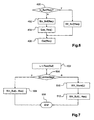
- the figure 6 shows a schema of the execution of an elected request Req transmitted from the input queue 114 to the cache 104.
- a step 400 it is first verified, thanks to the associated tag, that the corresponding data are not already present in the cache 104 (it is then a "cache hit” request) before making a new access in the bench If the memory area corresponding to the data is not represented in the cache 104 ("cache miss" request), a cache line is first released in order to allocate it to said memory zone, before making a memory cache. new access in the bank of memory 102.
- Sto_Buf () is a function Sto_Buf () in 402, explained in figure 7 .
- the Sto_Buf () function starts by designating in 502 a cache line L to be released.
- a test on the lock bit is performed to determine whether the line is releasable or not. In other words, if the previous request associated with said line was a read or write.
- the previous request associated with L was a read request, and the line L is therefore directly exploitable. Therefore, in the case where the current request is a write, the function Sto_Buf () starts at 506 write access to the cache with a function Wrt_Buf () and stores the data associated with the request in the line L. Then the Sto_Buf () function ends at 508 and the query execution continues at 404 with the Exe_Req () function.
- the previous request associated with L was a write request, so since the line is locked, it is first necessary to write the content of the line L in the memory bank. This is done at 510 by a Wrt_Mem () function that takes L as an argument, and writes the contents of that cache line into the matrix.
- the Exe_Req () function can be implemented in various ways.
- An example of an implementation consists in the case of a read to write the cache line L with the corresponding data of the memory bank.
- a "cache hit" when the current request is a write, the associated data can be directly written in line L.
- the function Out_Req () which is called at 406, merely receives data from the cache, and sends a "valid" to the output queue 118 to transmit the return data associated with the request that has just been sent. executed.
- the cache line which then represents the current state of the memory, and the update bit is then active.
- the first request is a write
- only the bytes to be written could be read directly.
- the associated row of the memory bank is accessed, and, by column, byte by byte, as a function of the byte validation bits, one will write then read selectively in the memory bank to update this and the cache line.
- the update bit enabled then indicates that all bytes represent the current state of the memory, all byte enable bits are disabled, and the lock bit since writes have been made.
- the device represented on the figure 8 is an embodiment optimized to take advantage of the advantages offered by the protocol described above.
- Each module 602 corresponds to the memory bank assembly 102, cache 104, sequencer 106, arbitration function 116, input queue 114, and output queue 118 of FIG. figure 3 .
- the memory bank 102 may contain a chosen number of memory arrays, and thus adapt the performance of the device to particular applications.
- the modules 602 are all connected to a power manager 604 whose role is to avoid current peaks (in the case where all the modules 602 try to access their respective bank 102 at the same time).
- Network agents Two network agents, namely an input agent 606 and an output agent 608 are connected to each of the nodes to distribute the load between the modules 602, and thus take advantage of the communication protocol and the multiplicity of modules 602.
- Network agents may be in the form of NoCs.
- a simple implementation of the input network agent is a one-input switch and n outputs (where n is the number of modules 602).
- a simple implementation of the output network agent is an n-input switch and an output.
- the agents 606 and 608 are respectively connected to a deserialization module 610 and to a serialization module 612, which makes it possible to have high speed serial links.
- the agents 606 and 608 may further be supplemented by other agents, which may for example make it possible to implement security or quality of service policies, as is possible thanks to the communication protocol.
Landscapes
- Engineering & Computer Science (AREA)
- Theoretical Computer Science (AREA)
- Physics & Mathematics (AREA)
- General Engineering & Computer Science (AREA)
- General Physics & Mathematics (AREA)
- Memory System Of A Hierarchy Structure (AREA)
- Dram (AREA)
Applications Claiming Priority (1)
| Application Number | Priority Date | Filing Date | Title |
|---|---|---|---|
| FR0706740A FR2921507B1 (fr) | 2007-09-26 | 2007-09-26 | Dispositif de memoire electronique |
Publications (3)
| Publication Number | Publication Date |
|---|---|
| EP2043103A2 true EP2043103A2 (de) | 2009-04-01 |
| EP2043103A3 EP2043103A3 (de) | 2009-11-11 |
| EP2043103B1 EP2043103B1 (de) | 2016-04-06 |
Family
ID=39283923
Family Applications (1)
| Application Number | Title | Priority Date | Filing Date |
|---|---|---|---|
| EP08290870.8A Ceased EP2043103B1 (de) | 2007-09-26 | 2008-09-16 | Elektronische Speichervorrichtung |
Country Status (3)
| Country | Link |
|---|---|
| US (1) | US7755920B2 (de) |
| EP (1) | EP2043103B1 (de) |
| FR (1) | FR2921507B1 (de) |
Families Citing this family (4)
| Publication number | Priority date | Publication date | Assignee | Title |
|---|---|---|---|---|
| US8713248B2 (en) * | 2009-06-02 | 2014-04-29 | Nokia Corporation | Memory device and method for dynamic random access memory having serial interface and integral instruction buffer |
| US8359438B2 (en) | 2010-05-18 | 2013-01-22 | Avago Technologies Enterprise IP (Singapore) Pte. Ltd. | Memory banking system and method to increase memory bandwidth via parallel read and write operations |
| US9251870B2 (en) * | 2013-04-04 | 2016-02-02 | Nvidia Corporation | Ground-referenced single-ended memory interconnect |
| US11556477B2 (en) * | 2018-06-15 | 2023-01-17 | Arteris, Inc. | System and method for configurable cache IP with flushable address range |
Citations (2)
| Publication number | Priority date | Publication date | Assignee | Title |
|---|---|---|---|---|
| FR2899413A1 (fr) | 2006-03-31 | 2007-10-05 | Arteris Sa | Systeme de commutation de message |
| FR2900017A1 (fr) | 2006-04-12 | 2007-10-19 | Arteris Sa | Systeme d'interconnexions de blocs fonctionnels externes sur puce muni d'un unique protocole parametrable de communication |
Family Cites Families (5)
| Publication number | Priority date | Publication date | Assignee | Title |
|---|---|---|---|---|
| JP3409866B2 (ja) * | 1992-09-18 | 2003-05-26 | 株式会社日立製作所 | 並列計算機 |
| US5802560A (en) * | 1995-08-30 | 1998-09-01 | Ramton International Corporation | Multibus cached memory system |
| JP3786521B2 (ja) * | 1998-07-01 | 2006-06-14 | 株式会社日立製作所 | 半導体集積回路及びデータ処理システム |
| US20030172189A1 (en) * | 2001-07-02 | 2003-09-11 | Globespanvirata Incorporated | Communications system using rings architecture |
| FR2863377B1 (fr) * | 2003-12-09 | 2006-02-17 | Arteris | Procede de gestion d'un dispositif de memorisation de donnees organisees en file d'attente, et dispositif associe |
-
2007
- 2007-09-26 FR FR0706740A patent/FR2921507B1/fr active Active
-
2008
- 2008-09-16 EP EP08290870.8A patent/EP2043103B1/de not_active Ceased
- 2008-09-25 US US12/284,820 patent/US7755920B2/en not_active Expired - Fee Related
Patent Citations (2)
| Publication number | Priority date | Publication date | Assignee | Title |
|---|---|---|---|---|
| FR2899413A1 (fr) | 2006-03-31 | 2007-10-05 | Arteris Sa | Systeme de commutation de message |
| FR2900017A1 (fr) | 2006-04-12 | 2007-10-19 | Arteris Sa | Systeme d'interconnexions de blocs fonctionnels externes sur puce muni d'un unique protocole parametrable de communication |
Also Published As
| Publication number | Publication date |
|---|---|
| US7755920B2 (en) | 2010-07-13 |
| EP2043103B1 (de) | 2016-04-06 |
| EP2043103A3 (de) | 2009-11-11 |
| FR2921507B1 (fr) | 2011-04-15 |
| US20090080280A1 (en) | 2009-03-26 |
| FR2921507A1 (fr) | 2009-03-27 |
Similar Documents
| Publication | Publication Date | Title |
|---|---|---|
| FR2779843A1 (fr) | Composant memoire multiport serie et application a un ordinateur | |
| EP3259674B1 (de) | Mit eingebautem prozessor ausgestattete dram-schaltung | |
| EP2043103B1 (de) | Elektronische Speichervorrichtung | |
| FR2827684A1 (fr) | Controleur de memoire presentant une capacite d'ecriture 1x/mx | |
| FR2881540A1 (fr) | Procede et systeme destines a empecher que des lignes de memoire cache soient videes jusqu'a ce que les donnees stockees dans celles-ci ne soient utilisees. | |
| FR2578071A1 (fr) | Installation de multitraitement a plusieurs processus | |
| FR2773233A1 (fr) | Circuit pour masquer des donnees et procede pour masquer des donnees d'un dispositif de memoire a semi-conducteurs | |
| WO2010070222A1 (fr) | Gestionnaire physique de barriere de synchronisation entre processus multiples | |
| FR2771209A1 (fr) | Dispositif de memoire a semiconducteur synchrone avec periode de latence programmable | |
| EP2088511A1 (de) | Multiprozessor-IT-System | |
| EP2438528A1 (de) | Verfahren und einrichtung zum laden und ausführen von anweisungen mit deterministischen zyklen in einem einen bus aufweisenden mehrkern-avioniksystem, dessen zugriffszeit unvorhersehbar ist | |
| EP0558125A1 (de) | Neuronalprozessor mit verteilten synaptischen Zellen | |
| FR3007542A1 (fr) | File d'echange de donnees ayant une profondeur illimitee | |
| FR2736779A1 (fr) | Appareil de commutation de donnees ,par exemple dans des reseaux a mode de transport asynchrone | |
| WO2022029026A1 (fr) | Module memoire reconfigurable adapte a mettre en oeuvre des operations de calcul | |
| EP1557767A1 (de) | Verfahren und System zur Nachrichtenübertragung in einem Verbindungsnetzwerk | |
| FR3048795A1 (fr) | Systeme sur puce et procede d'echange de donnees entre noeuds de calculs d'un tel systeme sur puce | |
| FR2824434A1 (fr) | Procede de diffusion d'un paquet de donnees au sein d'un reseau commute, base sur un calcul optimise de l'arbre de recouvrement | |
| FR2948785A1 (fr) | Terminateur de transaction | |
| EP1544724B1 (de) | Neue FIFO Speicherarkitektur und Betriebsverfahren für einen solchen Speicher | |
| EP0346420B1 (de) | Verfahren zum informationsaustausch in einem mehrprozessorsystem | |
| EP0822495B1 (de) | Auftragsverteilung in einem Mehrfachknoten-Rechnersystem | |
| EP0177429B1 (de) | Verfahren zum Informationsaustausch zwischen Teilnehmern mittels einer Busschleife und Anwendung in einem Multiprozessorgerät | |
| FR2769727A1 (fr) | Procede et systeme de controle d'acces partages a une memoire vive | |
| EP1033722B1 (de) | Gemeinsamer Speicher |
Legal Events
| Date | Code | Title | Description |
|---|---|---|---|
| PUAI | Public reference made under article 153(3) epc to a published international application that has entered the european phase |
Free format text: ORIGINAL CODE: 0009012 |
|
| AK | Designated contracting states |
Kind code of ref document: A2 Designated state(s): AT BE BG CH CY CZ DE DK EE ES FI FR GB GR HR HU IE IS IT LI LT LU LV MC MT NL NO PL PT RO SE SI SK TR |
|
| AX | Request for extension of the european patent |
Extension state: AL BA MK RS |
|
| PUAL | Search report despatched |
Free format text: ORIGINAL CODE: 0009013 |
|
| AK | Designated contracting states |
Kind code of ref document: A3 Designated state(s): AT BE BG CH CY CZ DE DK EE ES FI FR GB GR HR HU IE IS IT LI LT LU LV MC MT NL NO PL PT RO SE SI SK TR |
|
| AX | Request for extension of the european patent |
Extension state: AL BA MK RS |
|
| 17P | Request for examination filed |
Effective date: 20100419 |
|
| AKX | Designation fees paid |
Designated state(s): DE GB IT |
|
| 17Q | First examination report despatched |
Effective date: 20100630 |
|
| RAP1 | Party data changed (applicant data changed or rights of an application transferred) |
Owner name: QUALCOMM TECHNOLOGIES, INC. |
|
| GRAP | Despatch of communication of intention to grant a patent |
Free format text: ORIGINAL CODE: EPIDOSNIGR1 |
|
| INTG | Intention to grant announced |
Effective date: 20150605 |
|
| GRAP | Despatch of communication of intention to grant a patent |
Free format text: ORIGINAL CODE: EPIDOSNIGR1 |
|
| INTG | Intention to grant announced |
Effective date: 20151111 |
|
| GRAS | Grant fee paid |
Free format text: ORIGINAL CODE: EPIDOSNIGR3 |
|
| GRAA | (expected) grant |
Free format text: ORIGINAL CODE: 0009210 |
|
| AK | Designated contracting states |
Kind code of ref document: B1 Designated state(s): DE GB IT |
|
| REG | Reference to a national code |
Ref country code: GB Ref legal event code: FG4D Free format text: NOT ENGLISH |
|
| REG | Reference to a national code |
Ref country code: DE Ref legal event code: R096 Ref document number: 602008043289 Country of ref document: DE |
|
| PG25 | Lapsed in a contracting state [announced via postgrant information from national office to epo] |
Ref country code: IT Free format text: LAPSE BECAUSE OF FAILURE TO SUBMIT A TRANSLATION OF THE DESCRIPTION OR TO PAY THE FEE WITHIN THE PRESCRIBED TIME-LIMIT Effective date: 20160406 |
|
| REG | Reference to a national code |
Ref country code: DE Ref legal event code: R097 Ref document number: 602008043289 Country of ref document: DE |
|
| PLBE | No opposition filed within time limit |
Free format text: ORIGINAL CODE: 0009261 |
|
| STAA | Information on the status of an ep patent application or granted ep patent |
Free format text: STATUS: NO OPPOSITION FILED WITHIN TIME LIMIT |
|
| 26N | No opposition filed |
Effective date: 20170110 |
|
| PGFP | Annual fee paid to national office [announced via postgrant information from national office to epo] |
Ref country code: GB Payment date: 20170829 Year of fee payment: 10 |
|
| PGFP | Annual fee paid to national office [announced via postgrant information from national office to epo] |
Ref country code: DE Payment date: 20170928 Year of fee payment: 10 |
|
| REG | Reference to a national code |
Ref country code: DE Ref legal event code: R119 Ref document number: 602008043289 Country of ref document: DE |
|
| GBPC | Gb: european patent ceased through non-payment of renewal fee |
Effective date: 20180916 |
|
| PG25 | Lapsed in a contracting state [announced via postgrant information from national office to epo] |
Ref country code: DE Free format text: LAPSE BECAUSE OF NON-PAYMENT OF DUE FEES Effective date: 20190402 |
|
| PG25 | Lapsed in a contracting state [announced via postgrant information from national office to epo] |
Ref country code: GB Free format text: LAPSE BECAUSE OF NON-PAYMENT OF DUE FEES Effective date: 20180916 |