EP2043242A2 - Convertisseur de puissance avec haute dynamique et PFC - Google Patents
Convertisseur de puissance avec haute dynamique et PFC Download PDFInfo
- Publication number
- EP2043242A2 EP2043242A2 EP08253146A EP08253146A EP2043242A2 EP 2043242 A2 EP2043242 A2 EP 2043242A2 EP 08253146 A EP08253146 A EP 08253146A EP 08253146 A EP08253146 A EP 08253146A EP 2043242 A2 EP2043242 A2 EP 2043242A2
- Authority
- EP
- European Patent Office
- Prior art keywords
- power converter
- load current
- duty cycle
- voltage
- load
- Prior art date
- Legal status (The legal status is an assumption and is not a legal conclusion. Google has not performed a legal analysis and makes no representation as to the accuracy of the status listed.)
- Granted
Links
Images




Classifications
-
- H—ELECTRICITY
- H02—GENERATION; CONVERSION OR DISTRIBUTION OF ELECTRIC POWER
- H02M—APPARATUS FOR CONVERSION BETWEEN AC AND AC, BETWEEN AC AND DC, OR BETWEEN DC AND DC, AND FOR USE WITH MAINS OR SIMILAR POWER SUPPLY SYSTEMS; CONVERSION OF DC OR AC INPUT POWER INTO SURGE OUTPUT POWER; CONTROL OR REGULATION THEREOF
- H02M1/00—Details of apparatus for conversion
- H02M1/42—Circuits or arrangements for compensating for or adjusting power factor in converters or inverters
- H02M1/4208—Arrangements for improving power factor of AC input
- H02M1/4225—Arrangements for improving power factor of AC input using a non-isolated boost converter
-
- H—ELECTRICITY
- H02—GENERATION; CONVERSION OR DISTRIBUTION OF ELECTRIC POWER
- H02M—APPARATUS FOR CONVERSION BETWEEN AC AND AC, BETWEEN AC AND DC, OR BETWEEN DC AND DC, AND FOR USE WITH MAINS OR SIMILAR POWER SUPPLY SYSTEMS; CONVERSION OF DC OR AC INPUT POWER INTO SURGE OUTPUT POWER; CONTROL OR REGULATION THEREOF
- H02M3/00—Conversion of DC power input into DC power output
- H02M3/02—Conversion of DC power input into DC power output without intermediate conversion into AC
- H02M3/04—Conversion of DC power input into DC power output without intermediate conversion into AC by static converters
- H02M3/10—Conversion of DC power input into DC power output without intermediate conversion into AC by static converters using discharge tubes with control electrode or semiconductor devices with control electrode
- H02M3/145—Conversion of DC power input into DC power output without intermediate conversion into AC by static converters using discharge tubes with control electrode or semiconductor devices with control electrode using devices of a triode or transistor type requiring continuous application of a control signal
- H02M3/155—Conversion of DC power input into DC power output without intermediate conversion into AC by static converters using discharge tubes with control electrode or semiconductor devices with control electrode using devices of a triode or transistor type requiring continuous application of a control signal using semiconductor devices only
- H02M3/156—Conversion of DC power input into DC power output without intermediate conversion into AC by static converters using discharge tubes with control electrode or semiconductor devices with control electrode using devices of a triode or transistor type requiring continuous application of a control signal using semiconductor devices only with automatic control of output voltage or current, e.g. switching regulators
- H02M3/157—Conversion of DC power input into DC power output without intermediate conversion into AC by static converters using discharge tubes with control electrode or semiconductor devices with control electrode using devices of a triode or transistor type requiring continuous application of a control signal using semiconductor devices only with automatic control of output voltage or current, e.g. switching regulators with digital control
-
- Y—GENERAL TAGGING OF NEW TECHNOLOGICAL DEVELOPMENTS; GENERAL TAGGING OF CROSS-SECTIONAL TECHNOLOGIES SPANNING OVER SEVERAL SECTIONS OF THE IPC; TECHNICAL SUBJECTS COVERED BY FORMER USPC CROSS-REFERENCE ART COLLECTIONS [XRACs] AND DIGESTS
- Y02—TECHNOLOGIES OR APPLICATIONS FOR MITIGATION OR ADAPTATION AGAINST CLIMATE CHANGE
- Y02B—CLIMATE CHANGE MITIGATION TECHNOLOGIES RELATED TO BUILDINGS, e.g. HOUSING, HOUSE APPLIANCES OR RELATED END-USER APPLICATIONS
- Y02B70/00—Technologies for an efficient end-user side electric power management and consumption
- Y02B70/10—Technologies improving the efficiency by using switched-mode power supplies [SMPS], i.e. efficient power electronics conversion e.g. power factor correction or reduction of losses in power supplies or efficient standby modes
Definitions
- the present disclosure relates to power converters.
- a typical PFC boost rail for regulating a voltage of 390 volts often requires a 450 volt bulk capacitor because the voltage over shoot during a load dump could be as high as 430 volts.
- VRM voltage regulator module
- a method of controlling a power converter having at least one switching device for supplying an output voltage and a load current to a load includes sensing the output voltage, sensing the load current.
- the method also includes controlling a duty cycle of the switching device according to the sensed output voltage and a voltage control loop when a rate of change of the load current does not exceed a threshold level.
- the method further includes adjusting the duty cycle of the switching device set by the voltage control loop when the rate of change of the load current exceeds the threshold level.
- a power converter includes a controller and at least one switching device.
- the controller is configured to control a duty cycle of the switching device according to a sensed output voltage and a voltage control loop when a rate of change of a load current does not exceed a threshold level.
- the controller is also configured to adjust the duty cycle of the switching device set by the voltage control loop when the rate of change of the load current exceeds the threshold level.
- Fig. 1 is a circuit diagram of a power converter according to one embodiment including a PFC boost converter, a switching power supply, a controller and a sampling circuit.
- Fig. 2 is a circuit diagram of a voltage regulator module (VRM) system according to another embodiment of the present disclosure.
- VRM voltage regulator module
- Fig. 3 is a circuit diagram of an example analog implementation of a power converter including an analog circuit for adjusting the duty cycle of the power converter in response to a step load change.
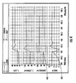
- Fig. 4 is a graph of the current and voltage effects of a step increase in load on the power converter in Fig. 3 without load current sensing.
- Fig. 5 is a graph of the current and voltage effects of a step increase in load on the power converter in Fig. 3 with load current sensing and proportional current control.
- Fig. 6 is a graph of the current and voltage effects of a step decrease in load on the power converter in Fig. 3 without load current sensing.
- Fig. 7 is a graph of the current and voltage effects of a step decrease in load on the power converter in Fig. 3 with load current sensing and proportional current control.
- Example embodiments are provided so that this disclosure will be thorough, and will fully convey the scope to those who are skilled in the art. Numerous specific details are set forth such as examples of specific components, devices, and methods, to provide a thorough understanding of embodiments of the present disclosure. It will be apparent to those skilled in the art that specific details need not be employed, that example embodiments may be embodied in many different forms and that neither should be construed to limit the scope of the disclosure. In some example embodiments, well-known processes, well-known device structures, and well-known technologies are not described in detail.
- first, second, third, etc. may be used herein to describe various elements, components, regions, layers and/or sections, these elements, components, regions, layers and/or sections should not be limited by these terms. These terms may be only used to distinguish one element, component, region, layer or section from another region, layer or section. Terms such as “first,” “second,” and other numerical terms when used herein do not imply a sequence or order unless clearly indicated by the context. Thus, a first element, component, region, layer or section discussed below could be termed a second element, component, region, layer or section without departing from the teachings of the example embodiments.
- a method of controlling a power converter having at least one switching device for supplying an output voltage and a load current to a load includes sensing the output voltage, sensing the load current.
- the method also includes controlling a duty cycle of the switching device according to the sensed output voltage and a voltage control loop when a rate of change of the load current does not exceed a threshold level.
- the method further includes adjusting the duty cycle of the switching device set by the voltage control loop when the rate of change of the load current exceeds the threshold level.
- the method can be used in any power converter topology having one or more switching devices where output current to a load can be sensed after the converter's bulk output capacitor.
- the method may be used in a power factor correction (PFC) boost regulator, a voltage regulation module (VRM) and/or a DC-DC converter.
- PFC power factor correction
- VRM voltage regulation module
- the method can, among other things, reduce voltage overshoot and undershoot.
- Example power converters for performing according to the aforementioned method will now be discussed with reference to Figs. 1-7 . It should be understood, however, that the method can be performed in a variety of other power converters without departing from the teachings of this disclosure.
- Fig. 1 illustrates a power supply, generally indicated by the reference numeral 100 according to at least one aspect of the present disclosure.
- the power supply includes a PFC boost power converter 102 for providing an output voltage, and current, to a load.
- the load is a switching power converter 104.
- An AC voltage from a voltage source 106 is rectified by a bridge rectifier 108 and input to the PFC boost power converter 102.
- the PFC boost power converter 102 provides power factor correction and supplies an output voltage that is input to the switching power converter 104.
- the switching power converter 104 supplies power to a load 110.
- a controller 112 samples the voltage supplied by the PFC boost power converter 102.
- the controller 112 may be an analog or a digital controller.
- the controller 112 controls, among other things, the switching duty cycle of switching devices, such as Q1, in the PFC boost power converter 102 in order to regulate the output voltage of the PFC boost power converter 102.
- a current in the power converter 102 is sampled at a second frequency. In some embodiments, the second frequency is greater than the first frequency at which the voltage is sampled. In Fig. 1 , the current is illustrated being sampled by a sampling circuit 114.
- the sampling circuit 114 may be a part of the controller 112, external circuitry or a combination of the two.
- the current is sensed using a series sense resistor 116 coupled to the converter 102 on the output side of a bulk output capacitor 118.
- Any other device capable of sensing the current such as a current transformer, Hall Effect sensor, etc., can also be used instead of, or along with, the sense resistor 116.
- the sampling circuit 114 can be a discrete circuit, part of the controller 112, or a combination of the controller 112 and parts external to the controller 112.
- the sampling circuit 114 may comprise external comparators which generate a logic level input to the controller 112 to indicate the level of the load current.
- the sampling circuit 114 may alternatively, or additionally, include comparators within the controller 112 (if available).
- the sampling circuit may also, or additionally, include a fast Analog to Digital converter (ADC) in the controller 112.
- ADC Analog to Digital converter
- the load current changes very quickly.
- Each sample of the current is compared to the previous sample.
- the sampling circuit 114 determines that the load is changing rapidly and that the duty cycle of the switching device Q1 should be adjusted in order to minimize voltage overshoot and undershoot.
- the maximum rate of current change that the PFC boost power converter 102 can provide is determined by, among other things, the duty cycle of the switching device Q1.
- adjusting the duty cycle changes how quickly the PFC boost power converter 102 can respond to the changing load and thereby changes how much voltage overshoot or undershoot is generated.
- the current is sampled at a frequency sufficient to detect changing current before the output voltage changes. This allows the controller 112 to respond quickly to the changing output current.
- the sampling circuit 114 determines an adjustment to the duty cycle of the switching device. This can be accomplished numerous ways.
- the sampling circuit 114 may include a predetermined lookup table that has been calibrated to provide a desired duty cycle adjustment based on one or more operating parameters such as input conditions, output voltage, output current and rate of change of output current.
- the adjustment to the duty cycle may also be determined by equation.
- the sampling circuit 114 overrides the duty cycle set by the voltage control loop of the controller 112 and adjusts the duty cycle according to the duty cycle adjustment previously determined. The duration of this adjustment can be set/determined in numerous ways.
- the duration can, for example, be a set length of time, a number of switching cycles, or can last until a steady state is achieved. Whichever manner of determining the duration is used, voltage control of the duty cycle is taken over again by the controller 112 when the duration of the adjustment ends.
- the adjusted duty cycle may be derived from two components.
- the first component is the duty cycle provided by the controller 112 based on, for example, a reference and the output voltage level. When the power converter 102 is operating at steady state, this is the only component for derivation of the adjusted duty cycle.
- the second component can be implemented by using the load current as an additional input to the controller 112 for calculating the duty cycle.
- the second component for the adjusted duty cycle can be provided by a non-linear component.
- the non-linear component will modify or replace the original duty cycle to achieve the adjusted duty cycle when the output current to the load changes rapidly.
- the determination of the amount to be added to (or subtracted from) the original duty cycle may be based on an equation or a look-up table.
- the equation or look-up table can be generated by simulation and then fine tuned by actual testing.
- the power supply 100 is operating in steady state at 50% load and drawing 2A of input current. If a step load is applied to the output off the power supply at a certain slew rate, it would result in a current slew rate on the input side that depends on the step-up or step-down ratio of the power supply. For example, if the load current steps from 50% to 100% at a rate that requires the input current to increase from 2A to 4A in 40 microseconds, it will result in a slew rate of 50 milliamps per microsecond.
- the bulk capacitor 118 While the current is increasing, the extra 2A of current required will be supplied by the bulk capacitor 118. Because the bulk capacitor 118 is chosen to have a large capacitance, it does not discharge appreciably in this time. However, there will be a small drop in the voltage input to the switching power converter 104 due to the equivalent series resistance (ESR) of the capacitor 118. Because the drop in voltage caused by the ESR of the capacitor is very small, the controller 112 may not recognize the change. Additionally, the controller 112 is sampling the voltage at a slow frequency. Thus, it will take some time before the controller 112 samples the voltage and recognizes that the voltage has changed. If the voltage is sampled at, for example 2kHz, the voltage is only sampled once every 500 microseconds.
- ESR equivalent series resistance
- the sampling circuit 114 is sampling the current at a frequency greater than the voltage sampling frequency. The exact frequency depends upon the controller 112, ADCs and/or other elements selected for the sampling circuit 114, but a frequency of 100kHz is a reasonable example. Therefore, the sampling circuit is sampling the current once every 10 microseconds and would acquire four samples during the 40 microseconds required for the current to reach 4A.
- each current sample is quite large as compared to the previous value.
- the sampling circuit 114 will determine a new duty cycle for the switch Q1. This sampling circuit 114 may determine the new duty cycle by retrieving the adjustment from a pre-calibrated look up table as discussed above. The sampling circuit then overrides the voltage control portion of the controller 112 to change or augment the duty cycle to the new duty cycle for a predetermined time.
- This adjusted duty cycle can be as high as 100%.
- the adjusted duty cycle will stay at this level for a certain duration as discussed above unless there is a substantial change in load current.
- voltage control of the duty cycle is taken over again by the controller 112 when the duration of the adjustment ends.
- the sample circuit 114 is operable to respond very quickly and decrease the duty cycle to help minimize voltage overshoot.
- the duty cycle of Q1 will be reduced for a certain duration as discussed above.
- the reduced duty cycle can be as low as a 0% duty cycle.
- the VRM 220 receives a DC input voltage and provides an output voltage to a load 210.
- the load is illustrated a microprocessor, but the load can be any load with which a VRM can be used.
- a controller 212 samples the output voltage supplied by the VRM 220 at a first frequency and an output current is sampled at a second frequency.
- the current is illustrated being sampled by a sampling circuit 214.
- the sampling circuit 214 may be a part of the controller 212, external circuitry or a combination of the two.
- the current is sensed using a series sense resistor 216. Any other device capable of sensing the current, such as a current transformer, Hall Effect sensor, etc., can also be used instead of, or along with, the sense resistor 216.
- the VRM 220 operates on a 12V input to produce an output voltage of 1.2V and delivers maximum load current of 20A. It operates at 1 MHz switching frequency and uses 0.2uH output inductor and is placed close to its load. The load can change current at a rate of 100A per microsecond. Specifications allow a maximum 50mV overshoot and/or undershoot in the voltage provided to the load.
- the ESR of output capacitor 218 is shown as resistor 222. The capacitor 218 is chosen such that its ESR is half the resistance of the sense resistor 216.
- the current sampling circuit 214 includes four comparator circuits configured to detect when load current changes in steps of 25% of the maximum possible change.
- the current detection signal from the sense resistor 216 can also be amplified using a precision, low offset differential amplifier and fed to an Analog to Digital Converter (ADC) of the controller 212 for processing.
- ADC Analog to Digital Converter
- a typical fast comparator and fast controller 212 can perform this task in 50 to 75 nanoseconds.
- the change in output current will occur in 150 nanoseconds.
- the comparators recognize the change in current and trigger an interrupt signal.
- the extra load current of 15A is supplied by the capacitor 218.
- the capacitor would discharge by 7mV. Because of the capacitor discharging, the voltage drop across the sense resistor 216, and the voltage drop across the resistor 222, the voltage provided to the load will decrease by approximately 22 mV.
- the controller 212 changes the duty cycle to nearly 100% and current in the VRM inductor 224 will start to increase. The rate of increase in current will depend on the value of the inductor.
- the current When 10.8V is applied across a 0.2uH inductor, the current will ramp up at the rate of 54A per microsecond. Thus, total ramp up from 5A to 20A would take 277nSec. During this time, the capacitor 218 will supply approximately half of the extra 15A current. This results in further discharge of the capacitor 218 to a voltage of 1.16V. Thus, the output voltage remains within the allowable 50 mV undershoot of the desired 1.2V.
- the current ramp rate in the inductor is predictable, and the modified duty cycle can be used for a predetermined length of time.
- the duty cycle is increased to approximately 100% for only 277 nanoseconds when the load switches from 5A to 20A. After that time, the controller is allowed to resume voltage control of the duty cycle.
- Fig. 3 illustrates an analog circuit 300 according to one or more aspects of the present disclosure for providing power to a load 310.
- the circuit 300 includes a power converter 326 providing an output voltage to the load 310.
- the circuit 300 includes a voltage error amplifier 328 for amplifying the error in the voltage supplied to the load 310.
- the circuit 300 further includes an integrated current sampling and control circuit 330.
- Fig. 4 graphically illustrates the effects of a step change in load on the output voltage of the power converter 326 of Fig. 3 if the current sampling and control circuit 330 is not used.
- the power converter 326 is subjected to a step load change from 30A to 60A at a rate of 5A per microsecond.
- this step change can be seen in a change in the voltage across a series sense resistor R4 in the power converter 326.
- the voltage output from the power converter 326 spikes down when the load changes suddenly.
- the voltage has dropped from 12 volts to 11.4 volts.
- the voltage increases until it overshoots the steady state 12 volts. This pattern continues until the current through the inductor and the output voltage reach a steady state again.
- Fig. 5 illustrates the effects of the same step load change on the circuit 300 in Fig. 3 when the current sampling and control circuit 330 is used.
- the power converter is subjected to the same 30A to 60A load change.
- the minimum value of the output voltage is approximately 11.65 volts.
- the voltage drop caused by the change in load is reduced by more than 0.2 volts as compared the results shown in Fig. 4 .
- Figures 6 and 7 similarly illustrate the response of the power converter 326 to a step decrease in load.
- the step change in the load is a decrease from 60A to 30A at a rate of 5A per microsecond.
- Fig. 6 illustrates the response when the current sampling and control circuit 330 is not used.
- the load change is evident in the change in voltage across the sense resistor R4 at 636.
- the voltage output from the power converter 326 spikes up from the steady state 12V output in response to the sudden change in load and peaks at 12.6V.
- the results of the power converter 326 being subjected to the same step decrease in load when the current sampling and control circuit 330 is used are shown in Fig. 7 .
- the change in load can bee seen in the voltage across the sense resistor R4 at 736.
- the output voltage of the power converter 326 spikes up from the steady state 12V at 738.
- the output voltage peaks below 12.4 volts.
- using the current sampling and control circuit 330 reduced the peak voltage overshoot by more than 0.2 volts.
Landscapes
- Engineering & Computer Science (AREA)
- Power Engineering (AREA)
- Dc-Dc Converters (AREA)
Applications Claiming Priority (2)
| Application Number | Priority Date | Filing Date | Title |
|---|---|---|---|
| US99705107P | 2007-09-28 | 2007-09-28 | |
| US12/236,798 US8232786B2 (en) | 2007-09-28 | 2008-09-24 | Fast transient step load response in a power converter |
Publications (3)
| Publication Number | Publication Date |
|---|---|
| EP2043242A2 true EP2043242A2 (fr) | 2009-04-01 |
| EP2043242A3 EP2043242A3 (fr) | 2015-01-07 |
| EP2043242B1 EP2043242B1 (fr) | 2021-05-12 |
Family
ID=40342498
Family Applications (1)
| Application Number | Title | Priority Date | Filing Date |
|---|---|---|---|
| EP08253146.8A Active EP2043242B1 (fr) | 2007-09-28 | 2008-09-26 | Convertisseur de puissance avec haute dynamique et PFC |
Country Status (2)
| Country | Link |
|---|---|
| US (1) | US8232786B2 (fr) |
| EP (1) | EP2043242B1 (fr) |
Cited By (5)
| Publication number | Priority date | Publication date | Assignee | Title |
|---|---|---|---|---|
| WO2011075531A3 (fr) * | 2009-12-19 | 2012-01-19 | Integrated Power Technology Corporation | Multiplexeur de commande pour alimentation à découpage |
| WO2013092847A1 (fr) * | 2011-12-23 | 2013-06-27 | Tridonic Gmbh & Co Kg | Procédé et circuit permettant de faire fonctionner des moyens d'éclairage à variation brusque de charge |
| WO2014004454A3 (fr) * | 2012-06-26 | 2014-06-26 | Analog Devices, Inc. | Commande d'alimentation électrique |
| TWI498704B (zh) * | 2012-11-06 | 2015-09-01 | 泰達電子公司 | 可動態調整輸出電壓之電源轉換器及其適用之供電系統 |
| AT15366U1 (de) * | 2016-04-07 | 2017-07-15 | Tridonic Gmbh & Co Kg | Verfahren und Schaltungsanordnung zum Betrieb von Leuchtmitteln |
Families Citing this family (26)
| Publication number | Priority date | Publication date | Assignee | Title |
|---|---|---|---|---|
| US8013474B2 (en) * | 2006-11-27 | 2011-09-06 | Xslent Energy Technologies, Llc | System and apparatuses with multiple power extractors coupled to different power sources |
| US9431828B2 (en) | 2006-11-27 | 2016-08-30 | Xslent Energy Technologies | Multi-source, multi-load systems with a power extractor |
| US7960870B2 (en) * | 2006-11-27 | 2011-06-14 | Xslent Energy Technologies, Llc | Power extractor for impedance matching |
| US8212399B2 (en) * | 2006-11-27 | 2012-07-03 | Xslent Energy Technologies, Llc | Power extractor with control loop |
| US7733073B2 (en) * | 2007-09-28 | 2010-06-08 | Infineon Technologies Ag | Current regulator with current threshold dependent duty cycle |
| US8344707B2 (en) * | 2008-07-25 | 2013-01-01 | Cirrus Logic, Inc. | Current sensing in a switching power converter |
| US8004260B2 (en) * | 2009-03-26 | 2011-08-23 | Delta Electronics, Inc. | Method and apparatus for multi-stage power supplies |
| JP5710870B2 (ja) * | 2009-09-28 | 2015-04-30 | ローランド株式会社 | Dc−dcコンバータ |
| US8972216B2 (en) * | 2010-03-09 | 2015-03-03 | Infineon Technologies Austria Ag | Methods and apparatus for calibration of power converters |
| KR101228799B1 (ko) | 2010-12-24 | 2013-01-31 | 한국과학기술원 | 전원공급장치 |
| KR101228767B1 (ko) * | 2010-12-24 | 2013-01-31 | 삼성전기주식회사 | 멀티 출력 스위칭모드 전원공급장치 |
| EP2509201B1 (fr) * | 2011-04-04 | 2016-03-30 | Nxp B.V. | Contrôleur pour alimentation électrique à découpage du type quasi-résonant |
| TWI443930B (zh) * | 2011-09-23 | 2014-07-01 | 亞旭電子科技(江蘇)有限公司 | 充電電流控制方法及充電系統 |
| WO2013097824A1 (fr) | 2011-12-31 | 2013-07-04 | 深圳市比亚迪汽车研发有限公司 | Véhicule électrique et système d'alimentation et régulateur de moteur pour véhicule électrique |
| US9608513B2 (en) | 2013-03-15 | 2017-03-28 | General Electric Company | Methods and systems for improving load transient response in LLC converters |
| JP6206162B2 (ja) * | 2013-12-19 | 2017-10-04 | 富士通株式会社 | Ac/dcコンバータおよびac/dc変換方法 |
| JP2016149903A (ja) * | 2015-02-13 | 2016-08-18 | トヨタ自動車株式会社 | 昇圧制御装置 |
| JP6455205B2 (ja) * | 2015-02-13 | 2019-01-23 | トヨタ自動車株式会社 | 昇圧制御装置 |
| CN106033936A (zh) * | 2015-03-09 | 2016-10-19 | 光宝电子(广州)有限公司 | 具有旁路功能的电源供应器及其操作方法 |
| EP3570423B1 (fr) * | 2018-05-14 | 2023-04-19 | Nxp B.V. | Dispositif de réponse de charge transitoire rapide pour alimentation en mode commuté |
| US10848066B1 (en) * | 2019-11-15 | 2020-11-24 | Hong Kong Applied Science and Technology Research Institute Company Limited | Controller for a DC/DC converter |
| WO2022187647A1 (fr) * | 2021-03-05 | 2022-09-09 | The Trustees Of Columbia University In The City Of New York | Systèmes et procédés pour des modes de réalisation de convertisseur de puissance à plusieurs niveaux empilés avec mise à l'échelle linéaire |
| CN113726144B (zh) * | 2021-07-15 | 2023-11-03 | 华为数字能源技术有限公司 | 驱动控制器、功率因数校正电路的控制系统及方法 |
| US12360139B2 (en) | 2022-08-10 | 2025-07-15 | Google Llc | Fast transient detection |
| CN116846203A (zh) * | 2023-01-12 | 2023-10-03 | 深圳威迈斯新能源股份有限公司 | 功率变换器逆变过流的防控方法以及保护装置 |
| US12438437B2 (en) | 2023-05-22 | 2025-10-07 | Apple Inc. | Dynamic control of AC-DC power converter PFC front end during load transients |
Family Cites Families (32)
| Publication number | Priority date | Publication date | Assignee | Title |
|---|---|---|---|---|
| US4885674A (en) * | 1988-03-28 | 1989-12-05 | Varga Ljubomir D | Synthesis of load-independent switch-mode power converters |
| EP0688076B1 (fr) | 1994-06-13 | 1997-11-12 | BULL HN INFORMATION SYSTEMS ITALIA S.p.A. | Alimentation avec correction du facteur de puissance et protection contre la défaillance de la correction du facteur de puissance |
| US5731692A (en) * | 1996-09-30 | 1998-03-24 | Lucent Technologies Inc. | System and method for limiting overshoot in a voltage and current control circuit |
| US5877611A (en) | 1996-10-09 | 1999-03-02 | Lucent Technologies Inc. | Simple and efficient switching regulator for fast transient loads such as microprocessors |
| US5929692A (en) * | 1997-07-11 | 1999-07-27 | Computer Products Inc. | Ripple cancellation circuit with fast load response for switch mode voltage regulators with synchronous rectification |
| DE19809385A1 (de) * | 1998-03-05 | 1999-09-09 | Bosch Gmbh Robert | Schaltregler |
| US6064187A (en) | 1999-02-12 | 2000-05-16 | Analog Devices, Inc. | Voltage regulator compensation circuit and method |
| US6087816A (en) | 1999-06-29 | 2000-07-11 | Maxim Integrated Products, Inc. | Step-up/step-down switching regulators and pulse width modulation control therefor |
| US6169669B1 (en) * | 1999-07-15 | 2001-01-02 | Texas Instruments Incorporated | Digital signal processor controlled uninterruptable power supply |
| US6147478A (en) | 1999-09-17 | 2000-11-14 | Texas Instruments Incorporated | Hysteretic regulator and control method having switching frequency independent from output filter |
| US6518738B1 (en) | 2000-03-29 | 2003-02-11 | Semiconductor Components Industries, Llc | Switching regulator control circuit with proactive transient response |
| US6605931B2 (en) | 2000-11-07 | 2003-08-12 | Microsemi Corporation | Switching regulator with transient recovery circuit |
| US6396252B1 (en) | 2000-12-14 | 2002-05-28 | National Semiconductor Corporation | Switching DC-to-DC converter with discontinuous pulse skipping and continuous operating modes without external sense resistor |
| US6965502B2 (en) * | 2001-03-21 | 2005-11-15 | Primarion, Inc. | System, device and method for providing voltage regulation to a microelectronic device |
| US6791302B2 (en) * | 2001-03-21 | 2004-09-14 | Primarion, Inc. | Methods and apparatus for open-loop enhanced control of power supply transients |
| US6472856B2 (en) * | 2001-03-09 | 2002-10-29 | Semtech Corporation | Bounded power supply voltage positioning |
| US6795009B2 (en) | 2002-09-09 | 2004-09-21 | Primarion, Inc. | System and method for current handling in a digitally-controlled power converter |
| US6696825B2 (en) * | 2002-03-18 | 2004-02-24 | Intersil Americas Inc. | DC-to-DC converter with fast override feedback control and associated methods |
| US6465994B1 (en) | 2002-03-27 | 2002-10-15 | Texas Instruments Incorporated | Low dropout voltage regulator with variable bandwidth based on load current |
| EP1367703A1 (fr) | 2002-05-31 | 2003-12-03 | STMicroelectronics S.r.l. | Méthode pour régler la tension d'alimentation d'une charge et régulateur de tension correspondant |
| JP4017490B2 (ja) | 2002-10-02 | 2007-12-05 | 株式会社デンソー | Dc/dcコンバータ |
| US6879138B2 (en) * | 2002-10-18 | 2005-04-12 | Intel Corporation | Buck converter with transient suppression |
| US6737846B1 (en) | 2002-12-17 | 2004-05-18 | Green Power Technologies Ltd. | Method and voltage feedback circuitry for improving the performance of APFC converters |
| TW595075B (en) | 2003-05-19 | 2004-06-21 | Richtek Technology Corp | DC to DC converter having fast transient-response of loading and method of the same |
| US6897641B1 (en) | 2004-06-24 | 2005-05-24 | Edward Herbert | Buck (or boost) converter with very fast output current transitions and low ripple voltage |
| TWI277850B (en) | 2004-08-27 | 2007-04-01 | Richtek Techohnology Corp | A spring type modulation circuit and method for voltage regulator |
| US7449869B2 (en) * | 2004-09-01 | 2008-11-11 | Artesyn Technologies, Inc. | Digital current mode controller with low frequency current sampling |
| EP1746712B1 (fr) * | 2005-07-19 | 2011-01-12 | STMicroelectronics Srl | Circuit de contrôle numérique non-linéaire et méthode pour un convertisseur continu-continu |
| US7323851B2 (en) * | 2005-09-22 | 2008-01-29 | Artesyn Technologies, Inc. | Digital power factor correction controller and AC-to-DC power supply including same |
| US7456618B2 (en) * | 2005-10-31 | 2008-11-25 | Chil Semiconductor, Inc. | Digital controller for a voltage regulator module |
| GB2436154B (en) * | 2006-03-10 | 2011-03-02 | Commergy Technologies Ltd | A power converter |
| US7615982B1 (en) * | 2006-07-26 | 2009-11-10 | Fairchild Semiconductor Corporation | Power converter able to rapidly respond to fast changes in load current |
-
2008
- 2008-09-24 US US12/236,798 patent/US8232786B2/en active Active
- 2008-09-26 EP EP08253146.8A patent/EP2043242B1/fr active Active
Cited By (12)
| Publication number | Priority date | Publication date | Assignee | Title |
|---|---|---|---|---|
| WO2011075531A3 (fr) * | 2009-12-19 | 2012-01-19 | Integrated Power Technology Corporation | Multiplexeur de commande pour alimentation à découpage |
| US8736243B2 (en) | 2009-12-19 | 2014-05-27 | Lanery Mgmt. Limited Liability Company | Control multiplexor for a switch mode power supply |
| WO2013092847A1 (fr) * | 2011-12-23 | 2013-06-27 | Tridonic Gmbh & Co Kg | Procédé et circuit permettant de faire fonctionner des moyens d'éclairage à variation brusque de charge |
| CN104025708A (zh) * | 2011-12-23 | 2014-09-03 | 赤多尼科两合股份有限公司 | 用于操作具有负载突变的发光机构的方法和电路布置结构 |
| US9445464B2 (en) | 2011-12-23 | 2016-09-13 | Tridonic Gmbh & Co Kg | Method and circuit arrangement for operating light-emitting means with a sudden load variation |
| CN104025708B (zh) * | 2011-12-23 | 2017-03-08 | 赤多尼科两合股份有限公司 | 用于操作具有负载突变的发光机构的方法和电路布置结构 |
| WO2014004454A3 (fr) * | 2012-06-26 | 2014-06-26 | Analog Devices, Inc. | Commande d'alimentation électrique |
| JP2015521839A (ja) * | 2012-06-26 | 2015-07-30 | アナログ・デバイシズ・インコーポレーテッド | 電源制御 |
| US9772636B2 (en) | 2012-06-26 | 2017-09-26 | Analog Devices, Inc. | Power supply control |
| TWI498704B (zh) * | 2012-11-06 | 2015-09-01 | 泰達電子公司 | 可動態調整輸出電壓之電源轉換器及其適用之供電系統 |
| US9535435B2 (en) | 2012-11-06 | 2017-01-03 | Delta Electronics (Thailand) Public Co., Ltd. | Power adapter for dynamically adjusting output voltage and power supply system with the same |
| AT15366U1 (de) * | 2016-04-07 | 2017-07-15 | Tridonic Gmbh & Co Kg | Verfahren und Schaltungsanordnung zum Betrieb von Leuchtmitteln |
Also Published As
| Publication number | Publication date |
|---|---|
| EP2043242B1 (fr) | 2021-05-12 |
| EP2043242A3 (fr) | 2015-01-07 |
| US8232786B2 (en) | 2012-07-31 |
| US20090085546A1 (en) | 2009-04-02 |
Similar Documents
| Publication | Publication Date | Title |
|---|---|---|
| US8232786B2 (en) | Fast transient step load response in a power converter | |
| US10797585B2 (en) | Multi-phase control for pulse width modulation power converters | |
| US8299773B2 (en) | System and method for limiting input-current surge in a switching mode power supply | |
| KR101131751B1 (ko) | 스위치 모드 전원 및 방법 | |
| JP6679851B2 (ja) | 力率改善コンバータ | |
| EP2680419B1 (fr) | Régulateurs de tension | |
| JP5790102B2 (ja) | 過渡変動抑圧機能を備えたデジタル制御式一体型dc−dcコンバータおよびその作動方法 | |
| US7986134B2 (en) | Power supplies, power supply controllers, and power supply controlling methods | |
| CN107659147B (zh) | 用于开关变换器的过流情况下的输出电压控制 | |
| US8198873B2 (en) | Power converter | |
| EP1779501A2 (fr) | Convertisseur cc-cc avec reglage adaptatif d'un parametre de commutation | |
| US20080030183A1 (en) | Method of feedback controlling a switched regulator | |
| US9431900B2 (en) | Dynamic operating frequency control of a buck power converter having a variable voltage output | |
| CN113783398A (zh) | 针对功率转换器的负载线调节 | |
| US9705405B2 (en) | Power converters and methods for reducing voltage changes at an output of a power converter | |
| US10175278B1 (en) | Detecting value of output capacitor in switching regulator | |
| US9906121B2 (en) | Control circuits and methods for transitioning between power converter control modes | |
| CN109660123A (zh) | 多相位电压调节器中的动态切换频率控制 | |
| US20080205087A1 (en) | Power supply feedback control using sensed duty cycle | |
| CN101436826B (zh) | 功率转换器中的快速暂态分步负载响应 | |
| CN111953191B (zh) | 具有稳态电流限制的dc-dc变换器 | |
| EP1274163A1 (fr) | Circuit pour une unité d' alimentation de puissance à découpage | |
| US20060025104A1 (en) | Dynamic trim to mitigate transients | |
| US20250202354A1 (en) | Non-linear transient improvements in current mode controllers | |
| GB2436154A (en) | Power factor pre-regulation stage for power converter |
Legal Events
| Date | Code | Title | Description |
|---|---|---|---|
| PUAI | Public reference made under article 153(3) epc to a published international application that has entered the european phase |
Free format text: ORIGINAL CODE: 0009012 |
|
| AK | Designated contracting states |
Kind code of ref document: A2 Designated state(s): AT BE BG CH CY CZ DE DK EE ES FI FR GB GR HR HU IE IS IT LI LT LU LV MC MT NL NO PL PT RO SE SI SK TR |
|
| AX | Request for extension of the european patent |
Extension state: AL BA MK RS |
|
| PUAL | Search report despatched |
Free format text: ORIGINAL CODE: 0009013 |
|
| AK | Designated contracting states |
Kind code of ref document: A3 Designated state(s): AT BE BG CH CY CZ DE DK EE ES FI FR GB GR HR HU IE IS IT LI LT LU LV MC MT NL NO PL PT RO SE SI SK TR |
|
| AX | Request for extension of the european patent |
Extension state: AL BA MK RS |
|
| RIC1 | Information provided on ipc code assigned before grant |
Ipc: H02M 3/157 20060101ALI20141128BHEP Ipc: H02M 1/42 20070101AFI20141128BHEP |
|
| 17P | Request for examination filed |
Effective date: 20150707 |
|
| RBV | Designated contracting states (corrected) |
Designated state(s): AT BE BG CH CY CZ DE DK EE ES FI FR GB GR HR HU IE IS IT LI LT LU LV MC MT NL NO PL PT RO SE SI SK TR |
|
| AKX | Designation fees paid |
Designated state(s): AT BE BG CH CY CZ DE DK EE ES FI FR GB GR HR HU IE IS IT LI LT LU LV MC MT NL NO PL PT RO SE SI SK TR |
|
| AXX | Extension fees paid |
Extension state: MK Extension state: RS Extension state: BA Extension state: AL |
|
| STAA | Information on the status of an ep patent application or granted ep patent |
Free format text: STATUS: EXAMINATION IS IN PROGRESS |
|
| 17Q | First examination report despatched |
Effective date: 20190327 |
|
| GRAP | Despatch of communication of intention to grant a patent |
Free format text: ORIGINAL CODE: EPIDOSNIGR1 |
|
| STAA | Information on the status of an ep patent application or granted ep patent |
Free format text: STATUS: GRANT OF PATENT IS INTENDED |
|
| INTG | Intention to grant announced |
Effective date: 20201216 |
|
| GRAS | Grant fee paid |
Free format text: ORIGINAL CODE: EPIDOSNIGR3 |
|
| GRAA | (expected) grant |
Free format text: ORIGINAL CODE: 0009210 |
|
| STAA | Information on the status of an ep patent application or granted ep patent |
Free format text: STATUS: THE PATENT HAS BEEN GRANTED |
|
| AK | Designated contracting states |
Kind code of ref document: B1 Designated state(s): AT BE BG CH CY CZ DE DK EE ES FI FR GB GR HR HU IE IS IT LI LT LU LV MC MT NL NO PL PT RO SE SI SK TR |
|
| REG | Reference to a national code |
Ref country code: GB Ref legal event code: FG4D |
|
| REG | Reference to a national code |
Ref country code: CH Ref legal event code: EP |
|
| REG | Reference to a national code |
Ref country code: DE Ref legal event code: R096 Ref document number: 602008063959 Country of ref document: DE |
|
| REG | Reference to a national code |
Ref country code: IE Ref legal event code: FG4D |
|
| REG | Reference to a national code |
Ref country code: AT Ref legal event code: REF Ref document number: 1392842 Country of ref document: AT Kind code of ref document: T Effective date: 20210615 |
|
| REG | Reference to a national code |
Ref country code: LT Ref legal event code: MG9D |
|
| REG | Reference to a national code |
Ref country code: AT Ref legal event code: MK05 Ref document number: 1392842 Country of ref document: AT Kind code of ref document: T Effective date: 20210512 |
|
| REG | Reference to a national code |
Ref country code: NL Ref legal event code: MP Effective date: 20210512 |
|
| PG25 | Lapsed in a contracting state [announced via postgrant information from national office to epo] |
Ref country code: BG Free format text: LAPSE BECAUSE OF FAILURE TO SUBMIT A TRANSLATION OF THE DESCRIPTION OR TO PAY THE FEE WITHIN THE PRESCRIBED TIME-LIMIT Effective date: 20210812 Ref country code: AT Free format text: LAPSE BECAUSE OF FAILURE TO SUBMIT A TRANSLATION OF THE DESCRIPTION OR TO PAY THE FEE WITHIN THE PRESCRIBED TIME-LIMIT Effective date: 20210512 Ref country code: HR Free format text: LAPSE BECAUSE OF FAILURE TO SUBMIT A TRANSLATION OF THE DESCRIPTION OR TO PAY THE FEE WITHIN THE PRESCRIBED TIME-LIMIT Effective date: 20210512 Ref country code: FI Free format text: LAPSE BECAUSE OF FAILURE TO SUBMIT A TRANSLATION OF THE DESCRIPTION OR TO PAY THE FEE WITHIN THE PRESCRIBED TIME-LIMIT Effective date: 20210512 Ref country code: LT Free format text: LAPSE BECAUSE OF FAILURE TO SUBMIT A TRANSLATION OF THE DESCRIPTION OR TO PAY THE FEE WITHIN THE PRESCRIBED TIME-LIMIT Effective date: 20210512 |
|
| PG25 | Lapsed in a contracting state [announced via postgrant information from national office to epo] |
Ref country code: LV Free format text: LAPSE BECAUSE OF FAILURE TO SUBMIT A TRANSLATION OF THE DESCRIPTION OR TO PAY THE FEE WITHIN THE PRESCRIBED TIME-LIMIT Effective date: 20210512 Ref country code: IS Free format text: LAPSE BECAUSE OF FAILURE TO SUBMIT A TRANSLATION OF THE DESCRIPTION OR TO PAY THE FEE WITHIN THE PRESCRIBED TIME-LIMIT Effective date: 20210912 Ref country code: GR Free format text: LAPSE BECAUSE OF FAILURE TO SUBMIT A TRANSLATION OF THE DESCRIPTION OR TO PAY THE FEE WITHIN THE PRESCRIBED TIME-LIMIT Effective date: 20210813 Ref country code: SE Free format text: LAPSE BECAUSE OF FAILURE TO SUBMIT A TRANSLATION OF THE DESCRIPTION OR TO PAY THE FEE WITHIN THE PRESCRIBED TIME-LIMIT Effective date: 20210512 Ref country code: PT Free format text: LAPSE BECAUSE OF FAILURE TO SUBMIT A TRANSLATION OF THE DESCRIPTION OR TO PAY THE FEE WITHIN THE PRESCRIBED TIME-LIMIT Effective date: 20210913 Ref country code: PL Free format text: LAPSE BECAUSE OF FAILURE TO SUBMIT A TRANSLATION OF THE DESCRIPTION OR TO PAY THE FEE WITHIN THE PRESCRIBED TIME-LIMIT Effective date: 20210512 Ref country code: NO Free format text: LAPSE BECAUSE OF FAILURE TO SUBMIT A TRANSLATION OF THE DESCRIPTION OR TO PAY THE FEE WITHIN THE PRESCRIBED TIME-LIMIT Effective date: 20210812 Ref country code: ES Free format text: LAPSE BECAUSE OF FAILURE TO SUBMIT A TRANSLATION OF THE DESCRIPTION OR TO PAY THE FEE WITHIN THE PRESCRIBED TIME-LIMIT Effective date: 20210512 |
|
| PG25 | Lapsed in a contracting state [announced via postgrant information from national office to epo] |
Ref country code: NL Free format text: LAPSE BECAUSE OF FAILURE TO SUBMIT A TRANSLATION OF THE DESCRIPTION OR TO PAY THE FEE WITHIN THE PRESCRIBED TIME-LIMIT Effective date: 20210512 |
|
| PG25 | Lapsed in a contracting state [announced via postgrant information from national office to epo] |
Ref country code: RO Free format text: LAPSE BECAUSE OF FAILURE TO SUBMIT A TRANSLATION OF THE DESCRIPTION OR TO PAY THE FEE WITHIN THE PRESCRIBED TIME-LIMIT Effective date: 20210512 Ref country code: DK Free format text: LAPSE BECAUSE OF FAILURE TO SUBMIT A TRANSLATION OF THE DESCRIPTION OR TO PAY THE FEE WITHIN THE PRESCRIBED TIME-LIMIT Effective date: 20210512 Ref country code: EE Free format text: LAPSE BECAUSE OF FAILURE TO SUBMIT A TRANSLATION OF THE DESCRIPTION OR TO PAY THE FEE WITHIN THE PRESCRIBED TIME-LIMIT Effective date: 20210512 Ref country code: CZ Free format text: LAPSE BECAUSE OF FAILURE TO SUBMIT A TRANSLATION OF THE DESCRIPTION OR TO PAY THE FEE WITHIN THE PRESCRIBED TIME-LIMIT Effective date: 20210512 Ref country code: SK Free format text: LAPSE BECAUSE OF FAILURE TO SUBMIT A TRANSLATION OF THE DESCRIPTION OR TO PAY THE FEE WITHIN THE PRESCRIBED TIME-LIMIT Effective date: 20210512 |
|
| REG | Reference to a national code |
Ref country code: DE Ref legal event code: R097 Ref document number: 602008063959 Country of ref document: DE |
|
| PLBE | No opposition filed within time limit |
Free format text: ORIGINAL CODE: 0009261 |
|
| STAA | Information on the status of an ep patent application or granted ep patent |
Free format text: STATUS: NO OPPOSITION FILED WITHIN TIME LIMIT |
|
| 26N | No opposition filed |
Effective date: 20220215 |
|
| REG | Reference to a national code |
Ref country code: BE Ref legal event code: MM Effective date: 20210930 |
|
| PG25 | Lapsed in a contracting state [announced via postgrant information from national office to epo] |
Ref country code: IS Free format text: LAPSE BECAUSE OF FAILURE TO SUBMIT A TRANSLATION OF THE DESCRIPTION OR TO PAY THE FEE WITHIN THE PRESCRIBED TIME-LIMIT Effective date: 20210912 Ref country code: MC Free format text: LAPSE BECAUSE OF FAILURE TO SUBMIT A TRANSLATION OF THE DESCRIPTION OR TO PAY THE FEE WITHIN THE PRESCRIBED TIME-LIMIT Effective date: 20210512 |
|
| PG25 | Lapsed in a contracting state [announced via postgrant information from national office to epo] |
Ref country code: LU Free format text: LAPSE BECAUSE OF NON-PAYMENT OF DUE FEES Effective date: 20210926 Ref country code: IT Free format text: LAPSE BECAUSE OF FAILURE TO SUBMIT A TRANSLATION OF THE DESCRIPTION OR TO PAY THE FEE WITHIN THE PRESCRIBED TIME-LIMIT Effective date: 20210512 Ref country code: FR Free format text: LAPSE BECAUSE OF NON-PAYMENT OF DUE FEES Effective date: 20210930 Ref country code: BE Free format text: LAPSE BECAUSE OF NON-PAYMENT OF DUE FEES Effective date: 20210930 |
|
| PG25 | Lapsed in a contracting state [announced via postgrant information from national office to epo] |
Ref country code: HU Free format text: LAPSE BECAUSE OF FAILURE TO SUBMIT A TRANSLATION OF THE DESCRIPTION OR TO PAY THE FEE WITHIN THE PRESCRIBED TIME-LIMIT; INVALID AB INITIO Effective date: 20080926 Ref country code: CY Free format text: LAPSE BECAUSE OF FAILURE TO SUBMIT A TRANSLATION OF THE DESCRIPTION OR TO PAY THE FEE WITHIN THE PRESCRIBED TIME-LIMIT Effective date: 20210512 |
|
| PGFP | Annual fee paid to national office [announced via postgrant information from national office to epo] |
Ref country code: DE Payment date: 20230802 Year of fee payment: 16 |
|
| PG25 | Lapsed in a contracting state [announced via postgrant information from national office to epo] |
Ref country code: TR Free format text: LAPSE BECAUSE OF FAILURE TO SUBMIT A TRANSLATION OF THE DESCRIPTION OR TO PAY THE FEE WITHIN THE PRESCRIBED TIME-LIMIT Effective date: 20210512 |
|
| REG | Reference to a national code |
Ref country code: DE Ref legal event code: R231 Ref document number: 602008063959 Country of ref document: DE |
|
| PG25 | Lapsed in a contracting state [announced via postgrant information from national office to epo] |
Ref country code: MT Free format text: LAPSE BECAUSE OF FAILURE TO SUBMIT A TRANSLATION OF THE DESCRIPTION OR TO PAY THE FEE WITHIN THE PRESCRIBED TIME-LIMIT Effective date: 20210512 |
|
| PG25 | Lapsed in a contracting state [announced via postgrant information from national office to epo] |
Ref country code: DE Free format text: LAPSE BECAUSE OF THE APPLICANT RENOUNCES Effective date: 20240916 |
|
| PG25 | Lapsed in a contracting state [announced via postgrant information from national office to epo] |
Ref country code: DE Free format text: LAPSE BECAUSE OF THE APPLICANT RENOUNCES Effective date: 20240916 |
|
| REG | Reference to a national code |
Ref country code: CH Ref legal event code: U11 Free format text: ST27 STATUS EVENT CODE: U-0-0-U10-U11 (AS PROVIDED BY THE NATIONAL OFFICE) Effective date: 20251001 |
|
| PGFP | Annual fee paid to national office [announced via postgrant information from national office to epo] |
Ref country code: GB Payment date: 20250703 Year of fee payment: 18 |
|
| PGFP | Annual fee paid to national office [announced via postgrant information from national office to epo] |
Ref country code: IE Payment date: 20250702 Year of fee payment: 18 |
|
| PGFP | Annual fee paid to national office [announced via postgrant information from national office to epo] |
Ref country code: CH Payment date: 20251001 Year of fee payment: 18 |