EP2044423B1 - Vorrichtung und verfahren zur oberflächencharakterisierung - Google Patents
Vorrichtung und verfahren zur oberflächencharakterisierung Download PDFInfo
- Publication number
- EP2044423B1 EP2044423B1 EP07803851.0A EP07803851A EP2044423B1 EP 2044423 B1 EP2044423 B1 EP 2044423B1 EP 07803851 A EP07803851 A EP 07803851A EP 2044423 B1 EP2044423 B1 EP 2044423B1
- Authority
- EP
- European Patent Office
- Prior art keywords
- molecules
- neutral atoms
- atoms
- energy
- generating
- Prior art date
- Legal status (The legal status is an assumption and is not a legal conclusion. Google has not performed a legal analysis and makes no representation as to the accuracy of the status listed.)
- Active
Links
Images

Classifications
-
- G—PHYSICS
- G01—MEASURING; TESTING
- G01N—INVESTIGATING OR ANALYSING MATERIALS BY DETERMINING THEIR CHEMICAL OR PHYSICAL PROPERTIES
- G01N23/00—Investigating or analysing materials by the use of wave or particle radiation, e.g. X-rays or neutrons, not covered by groups G01N3/00 – G01N17/00, G01N21/00 or G01N22/00
- G01N23/20—Investigating or analysing materials by the use of wave or particle radiation, e.g. X-rays or neutrons, not covered by groups G01N3/00 – G01N17/00, G01N21/00 or G01N22/00 by using diffraction of the radiation by the materials, e.g. for investigating crystal structure; by using scattering of the radiation by the materials, e.g. for investigating non-crystalline materials; by using reflection of the radiation by the materials
- G01N23/201—Investigating or analysing materials by the use of wave or particle radiation, e.g. X-rays or neutrons, not covered by groups G01N3/00 – G01N17/00, G01N21/00 or G01N22/00 by using diffraction of the radiation by the materials, e.g. for investigating crystal structure; by using scattering of the radiation by the materials, e.g. for investigating non-crystalline materials; by using reflection of the radiation by the materials by measuring small-angle scattering
-
- G—PHYSICS
- G01—MEASURING; TESTING
- G01N—INVESTIGATING OR ANALYSING MATERIALS BY DETERMINING THEIR CHEMICAL OR PHYSICAL PROPERTIES
- G01N23/00—Investigating or analysing materials by the use of wave or particle radiation, e.g. X-rays or neutrons, not covered by groups G01N3/00 – G01N17/00, G01N21/00 or G01N22/00
- G01N23/20—Investigating or analysing materials by the use of wave or particle radiation, e.g. X-rays or neutrons, not covered by groups G01N3/00 – G01N17/00, G01N21/00 or G01N22/00 by using diffraction of the radiation by the materials, e.g. for investigating crystal structure; by using scattering of the radiation by the materials, e.g. for investigating non-crystalline materials; by using reflection of the radiation by the materials
- G01N23/20058—Measuring diffraction of electrons, e.g. low energy electron diffraction [LEED] method or reflection high energy electron diffraction [RHEED] method
-
- G—PHYSICS
- G01—MEASURING; TESTING
- G01N—INVESTIGATING OR ANALYSING MATERIALS BY DETERMINING THEIR CHEMICAL OR PHYSICAL PROPERTIES
- G01N23/00—Investigating or analysing materials by the use of wave or particle radiation, e.g. X-rays or neutrons, not covered by groups G01N3/00 – G01N17/00, G01N21/00 or G01N22/00
- G01N23/20—Investigating or analysing materials by the use of wave or particle radiation, e.g. X-rays or neutrons, not covered by groups G01N3/00 – G01N17/00, G01N21/00 or G01N22/00 by using diffraction of the radiation by the materials, e.g. for investigating crystal structure; by using scattering of the radiation by the materials, e.g. for investigating non-crystalline materials; by using reflection of the radiation by the materials
- G01N23/207—Diffractometry using detectors, e.g. using a probe in a central position and one or more displaceable detectors in circumferential positions
Definitions
- the invention relates to a device and a method for surface characterization.
- it makes it possible to determine the crystallographic structure of crystalline surfaces and to monitor, in real time, the growth of crystals by molecular beam epitaxy.
- the most commonly used techniques for determining the crystallographic structure of surfaces are Low Energy Electron Diffraction (LEED) and Fast Reflective Electron Diffraction (RHEED). ). See for example EP 1 401 007 .
- the RHEED technique has the very important advantage of being compatible with the growth of crystals by molecular beam epitaxy; in fact, molecular beam epitaxy devices generally include an integrated RHEED device.
- the latter essentially consists of an electron gun, arranged to produce a substantially monocinetic beam of electrons having an energy of the order of 5 - 50 keV directed towards the surface to be studied with an angle of incidence of order of 1 ° - 4 ° with respect to the plane of the surface, a phosphor screen allowing the visualization of electrons diffracted towards the front by the surface and a camera to acquire images of said phosphor screen.
- the RHEED technique allows a complete characterization of the crystallographic structure of a surface, provided that acquisitions are made corresponding to at least two distinct orientations of said surface. However, very often, one limits oneself to a qualitative characterization of the state of a surface compared to a reference diffraction figure.
- Another important application of the RHEED technique is the real-time monitoring of layer-by-layer growth of a crystal by molecular beam epitaxy. Indeed, when a layer has just been completed, the diffraction peaks are clearly visible and have a high contrast; as more atoms are deposited on this layer the contrast is degraded, for increase again when these atoms are numerous enough to form a new layer. Oscillations of the diffraction signal are thus observed, which enable the formation of the different atomic layers of the crystal to be followed in time.
- the electrons even at grazing incidence, have a penetration power of several Angstroms, which means that they are not sensitive only to the first atomic layer, constituting the surface in the strict sense, but also to the first sub-layers. underlying. Moreover, the penetration of electrons below the surface often results in a complex diffraction pattern that is difficult to interpret.
- the low energy neutral atoms are extremely difficult to detect. Detection is usually done point by point using a mass spectrometer that is moved in two dimensions. The formation of a diffraction pattern therefore requires a considerable time, incompatible with an online control.
- An object of the present invention is to overcome at least some of the disadvantages of the prior art.
- an object of the invention is to provide a surface characterization technique having increased sensitivity to the first atomic layer compared to RHEED and LEED techniques.
- Another object of the invention is to provide a characterization technique better suited to insulating surfaces than the techniques known from the prior art.
- Yet another object of the invention is to provide a surface characterization technique compatible with growth by molecular beam epitaxy and allowing real-time control of said growth.
- Yet another object of the invention is to provide a surface characterization technique that is simple to implement, not only in the laboratory, but also in an industrial environment.
- Another object of the invention is a machine for molecular beam epitaxy comprising a surface characterization device according to one of the preceding claims, arranged to characterize the surface of a crystal in the course of growth.
- a device consists essentially of a means 1 for generating a beam 2 of neutral atoms or molecules and a sensing means 3 responsive in position of said beam of neutral atoms or molecules.
- the beam 2 is directed towards a surface 3 to be characterized according to an angle of incidence ⁇ inc , possibly variable, not greater than about 10 ° (grazing incidence); here and in the following, the angles are measured relative to the plane of the target surface 3.
- ⁇ inc possibly variable, not greater than about 10 ° (grazing incidence); here and in the following, the angles are measured relative to the plane of the target surface 3.
- the neutral atoms or molecules of the beam 2 are reflected by said surface 3, with a reflection angle ⁇ ref ⁇ inc ; at the same time they undergo a diffraction in an azimuthal direction, ie parallel to the surface 3.
- the incident atomic or molecular beam is indicated by the reference 2-i, the specular beam by 2-0 (because it is the "zero order" of diffraction) and the first non-specular beam by 2-1 (first order of diffraction).
- the diffracted beams 2-0 and 2-1 are detected, at a distance from the surface 3, by the position-sensitive detection means 4, which forms an image of the diffraction pattern, which makes it possible to measure the angle ⁇ and therefore determine the mesh parameter a.
- the high-energy particles used in the process of the invention can be detected simply, for example by microchannel plates (MCPs) coupled to a phosphor screen which is in turn imaged by a CCD camera.
- MCPs microchannel plates
- Figure 1A is a simplification, because in general several orders of diffraction are simultaneously observed, as well as an incoherent background due to structural defects of the surface (steps, adsorbed atoms, etc.), as well as thermal vibrations.
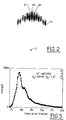
- the figure 2 shows a real example of a diffraction pattern obtained by directing H 2 molecules of 400 eV energy on a ZnSe (001) surface in the crystallographic direction [1 -1 0] with an angle of incidence of 1, 1.
- the references D0, D-1 and D1 highlight the central spot corresponding to the zero order, and the first two orders arranged symmetrically around it.
- the spacing between the diffraction spots gives information on the periodicity of the crystalline lattice of the surface (parameter of mesh a), this is true for all the diffraction techniques, see for example the structure of DP Woodruff and TA Delchar "Modern techniques of surface science", Cambridge University Press, 1986 , while their relative intensity provides information on the shape of the interaction potential between the projectile and the surface. It is observed that the diffraction spots are arranged along a curve CD, whose shape depends on the form of said interaction potential, the normal energy E n of the projectile and the temperature. For a non-reactive projectile, the curve CD is an arc whose circle passes through the projected plane of the surface.
- a spot S produced by the particles of the beam 2 which flew over the surface 3 without interacting.
- the observation of the spot S does not bring any information directly related to the properties of said surface, but can be exploited to determine the angles of incidence and diffusion and to calibrate the loss of energy in the flight time measurements in the case of a pulsed beam.
- H is the projectile of lower mass, and its use makes it possible to study the interaction potential of the surface with hydrogen, which is very interesting in many applications.
- 3 He will be preferred when one wishes to have a chemically inert projectile while H 2 , whose mass and reactivity are intermediate between those of H and 3 He, may constitute a compromise solution.
- He 3 He or 4 He is the preferred projectile.
- the energy E 0 of the beam may be between about 50 eV and about 5 keV, preferably between 100 eV and 2 keV and still more preferably between 100 eV and 1 keV. It is preferable that the dispersion of the energy of the beam is less than or equal to 5%, preferably less than or equal to 2%.
- the angle of incidence relative to the plane of the surface, ⁇ inc must be less than or equal to 10 °, preferably between 0.5 ° and 3 °.
- E n E 0 sin 2 ⁇ inc be less than or equal to 1 eV.
- the divergence of the beam must be minimized because it has a tendency to scramble the diffraction peaks: typically to obtain images of good quality it is necessary to obtain a divergence of no more than 0.05 °.
- the size of the beam is less than or equal to 1 mm, preferably between 10 and 300 ⁇ m approximately.
- the size of the beam in a direction parallel to the surface has a direct influence on the size of the diffraction spots at the detector 3; if the beam is too wide, these spots tend to be superimposed and this results in a scrambling of the diffraction pattern.
- the width of the beam in a direction normal to the surface is less critical, but it must be considered that, because of the grazing incidence, the projection on the surface of this dimension of the beam is stretched by a factor 1 / sin ⁇ inc , and can therefore easily exceed the size of the sample. It is therefore preferable to limit it to a value of less than or equal to 1 mm. As a rule, it is preferred to use at least approximately circular section beams.
- the flow does not have to be very important: with a flow of a few hundred atoms per second only, a few minutes of exposure are enough to obtain directly exploitable images.
- the temperature of the sample is another parameter that has to be taken into account because the thermal agitation of the surface atoms adversely affects the diffraction efficiency. It is therefore advantageous for the sample to be kept at ambient temperature (around 300 K) during the measurement. It is generally not necessary to cool the sample to cryogenic temperatures, although this may improve the quality of the diffraction pattern obtained. If the temperature is imposed, for example by the epitaxial growth method, it is possible to limit the effect of the thermal agitation by choosing a smaller angle of incidence: in fact, the lower the incidence, the more the diffusion takes place far from the surface, and therefore the less the projectile is sensitive to the periodicity defects induced by the thermal agitation.
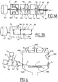
- a means of generating an ion beam or molecules adapted to the implementation of the invention is represented on the figure 3A .
- This device essentially consists of a generator of a beam 2 'of atomic or molecular ions 11, a neutraliser 14 and a collimator 15.
- ion sources 11 there are several types of ion sources 11 that are suitable for the implementation of the invention, providing ion beams having an energy of between a few eV and a few keV.
- ECR cyclotron electron resonance
- the ion source 11 comprises a set of electrodes for accelerating the ions to the desired energy by applying an electrostatic field, as well as focusing electrostatic optics.
- the ion beam generated by the source 11 is not sufficiently pure from the chemical and isotopic point of view, or if it contains ions of different states of charge, it can be directed to a mass filter 12 which uses a magnetic field generated by a magnet 121 and a slot 122 to select particles having a mass-to-charge ratio determined. Although this is not visible on the figure 3A , a filter of Magnetic mass of this type is not in a straight line and necessarily introduces a deviation of the beam 2 'of ions.
- a chopper 13 may be provided, whether upstream or downstream of the optional mass filter.
- the device comprises an inlet slot 131 for the shaping the beam, two plate-like electrodes 132, 132 'facing each other and an outlet port 133.
- the electric charge of the ions makes it possible to accelerate, select and pulse them much more easily than neutral particles.
- the gas used in the cell 14 consists of the same chemical species of the beam 2 in order to optimize the charge exchange by resonant capture; the pressure P 14 inside the cell depends on its length L 14 and in general we put P 14 x L 14 ⁇ 10 -3 mbar ⁇ cm.
- an electrostatic field applied by electrodes 141, 141 ' makes it possible to deflect the remaining ions, so that only one beam 2 of neutral atoms or molecules leaves the cell 14.
- a collimator 15 may simply consist of a first and a second diaphragm, D1 and D2, preferably circular, having diameters ⁇ D1 and D2 D2 of the same order of magnitude, aligned on the axis of the beam and spaced d a distance L.
- Div ( ⁇ D1 + ⁇ D2 ) / 2L.
- Div ( ⁇ D1 + ⁇ D2 ) / 2L.
- Div ( ⁇ D1 + ⁇ D2 ) / 2L.
- Div ( ⁇ D1 + ⁇ D2 ) / 2L.
- ⁇ D1 and ⁇ D2 of the order of 100 to 200 microns and L between 20 and 30 cm.
- the figure 3B shows a simplified and much more compact variant of a means 1 for generating an atomic or molecular beam.
- This simplified device has neither mass filter 12 nor chopper 13.
- the neutralization cell 14 is constituted by a section of a tubular element 16 between two diaphragms D0 and D1, the diameter of the diaphragm D0 being much larger than that of the diaphragm D1.
- the cell 14 comprises a gas inlet 145 and is surrounded by a chamber 146 connected to a vacuum pumping system not shown; the electrodes 141, 141 'intended to deflect the non-recombined ions are disposed inside said tubular element 16, downstream of the diaphragm D1.
- the latter in addition to delimiting the neutralization cell 14, is part of the collimator 15, just like the diaphragm, D2 located at the outlet of the tubular element 15.
- the device of the figure 3B can not produce a pulsed beam 2 of neutral atoms or molecules. It can nevertheless produce a pulsed ion beam 2 ': for this it suffices to evacuate the neutralization cell 14 and to apply a pulsed voltage to the electrodes 141, 141' so as to use them as a chopper.
- the figure 4 shows a machine for molecular beam epitaxy 1000 equipped with a surface characterization device according to the invention.
- the machine 1000 consists essentially of a chamber 1100 connected to a pumping system (not shown) which produces an ultrahigh vacuum.
- a pumping system not shown
- In the enclosure 1100 emit 1200 effusion cells that produce molecular beams.
- In front of these cells 1200 is located a support 1300 for a substrate 3 'on which the surface 3 must be deposited by epitaxy.
- the user can choose to characterize the surface using the atomic or molecular beam 2 according to the invention, or by the traditional RHEED technique, without it being necessary to provide an additional input in the enclosure 1000. More precisely, when one wishes to perform a RHEED characterization, only the electron gun 20 is activated, while the ion source 11 and the deflector 30 remain inactive, and the neutralization cell 14 is evacuated.
- the electron gun 20 remains inactive, while the ion source 11 and the deflector 30 are active and the neutralization cell is filled with gas.
- the deflector 30 can be obtained a pulsed atom or molecule beam: in this case the deflector 30 can be used as a chopper.
- Position-sensitive detection means 4 constituted by a microchannel slab coupled to a fluorescent screen, is also arranged in the wall of the enclosure 1100, in a position opposite to that of the generation means 1 with respect to the surface 3.
- the means 4 is also adapted to the detection of electrons, it is therefore compatible with the RHEED technique.
- the characterization device of the invention can completely replace a device RHEED.
- the angle of incidence ⁇ inc of the beam 2 on the surface 3 can be varied, for example in the range 0.5 ° -10 °, in order to allow a more complete characterization of said surface (so-called "rocking curves"). This can be achieved, for example, by mounting the generation means 1 with a motorized swivel mechanism. As a variant, if only a qualitative control of the quality of the surface 3 is required, the angle ⁇ inc can be fixed.
- the device of the invention allows real-time monitoring of the growth of conductive or dielectric surfaces, while the RHEED technique is poorly adapted to dielectric surfaces.
- the diffraction of fast atoms in grazing incidence makes it possible to obtain diffraction patterns that are easier to interpret than the RHEED figures, because of the low penetration power of the atoms or molecules beneath the surface to be studied.
- the device and the method of the invention are not limited to providing information of a crystallographic nature: they allow a much more complete characterization of the surfaces.
- the detector 4 it is necessary for the detector 4 to have a sufficient temporal resolution to allow a measurement of the energy of the particles scattered by flight, for example of the order of 50 ns or less, and preferably of the order of 10 ns or less.
- the x-axis of the figure 5 carries the time of flight of atoms, expressed in arbitrary units; a calibration of the instrument allows to associate with each flight time a value of the energy of the atoms after diffusion by the surface.
- a calibration of the instrument allows to associate with each flight time a value of the energy of the atoms after diffusion by the surface.
- a similar technique can be used to determine the concentration of light particles adsorbed on the surface 3.
- These particles mainly hydrogen atoms
- the flight time of these ejected particles makes it possible to determine their mass, and therefore to identify them.
- the heavy species present on the surface can not be ejected by the beam projectiles 2, much lighter; on the other hand, they produce a wide-angle diffusion with a loss of energy of said projectiles. In this case, it is the measurement of the flight time of the scattered projectiles which makes it possible to determine the mass of the adsorbed particles, and thus to identify them.
- a secondary detector for measuring the flight time of the particles ejected from the surface 3 following a collision with a projectile of the beam 2, as well as projectiles of said beam scattered at wide angle is shown schematically under the reference 1600.
- the detector 1600 must have a temporal resolution of no greater than 1 ⁇ s, preferably no greater than 100 ns and still more preferably no greater than 10 ns.
- it is arranged in such a way as to detect neutral or ionized atoms or molecules which leave the surface to be characterized along a path which forms with said surface 3 an angle greater than the specular reflection angle of the beam of neutral atoms or molecules. for example an angle of about 30 °.
- the identification of the adsorbed particles can also be performed using ions as projectiles. This makes it possible to use, even in this application, the beam generation means of the figure 3B which can not produce a neutral pulse beam.
- the same means 1 for generating an atomic or molecular beam can be used both for performing surface diffraction measurements and for identifying the adsorbed particles.
- the same means 1 for generating an atomic or molecular beam can be used both for performing surface diffraction measurements and for identifying the adsorbed particles.
- the identification of the adsorbed particles advantageously combines with the observation of diffraction patterns for real-time monitoring of crystal growth by epitaxy.
- the study of the oscillations of the diffraction peaks makes it possible to follow the evolution of the deposition of successive atomic layers, as is commonly done using the RHEED technique, while the detection particles leaving the surface 3 following a collision with an atom or molecule of the beam 2 (or an ion of the beam 2 '), as well as projectiles scattered at great angles following a collision with a heavy adsorbed particle, allows to know the level of contamination of this same surface.
- the chopping of the beam 2 or 2 ' considerably reduces its flux, and thus makes the diffraction patterns little visible, the two types of measurement will generally be alternated in time.
Landscapes
- Chemical & Material Sciences (AREA)
- Biochemistry (AREA)
- General Physics & Mathematics (AREA)
- Health & Medical Sciences (AREA)
- Life Sciences & Earth Sciences (AREA)
- Analytical Chemistry (AREA)
- Crystallography & Structural Chemistry (AREA)
- General Health & Medical Sciences (AREA)
- Physics & Mathematics (AREA)
- Immunology (AREA)
- Pathology (AREA)
- Analysing Materials By The Use Of Radiation (AREA)
- Physical Vapour Deposition (AREA)
- Physical Deposition Of Substances That Are Components Of Semiconductor Devices (AREA)
- Investigating Materials By The Use Of Optical Means Adapted For Particular Applications (AREA)
Claims (18)
- Vorrichtung zur Oberflächencharakterisierung, Folgendes beinhaltend:- Mittel (1) zur Erzeugung eines Strahls (2) von neutralen Atomen oder Molekülen, angeordnet, um den Strahl (2) auf eine zu charakterisierende Oberfläche (3) zu richten; und- positionsempfindliche Detektionsmittel (4) zur Detektion der Atome oder Moleküle des Strahls (2), welche von der zu charakterisierenden Oberfläche (3) nach vorn verstreut werden;dadurch gekennzeichnet, dass- die Mittel (1) zur Erzeugung eines Strahls (2) von neutralen Atomen oder Molekülen geeignet sind, um einen Strahl (2) zu erzeugen, der eine Energie zwischen 50 eV und 5 keV und eine Divergenz von nicht über 0,05° besitzt; und- dass die Mittel (1) zur Erzeugung eines Strahls von neutralen Atomen oder Molekülen geeignet sind, um den Strahl (2) auf die zu charakterisierende Oberfläche (3) mit einem Einfallwinkel von nicht über 10° in Bezug auf die Ebene der Oberfläche (3) zu richten;in der Weise, dass ein Diffraktionsbild der von der zu charakterisierenden Oberfläche (3) nach vorn verstreuten neutralen Atome oder Moleküle durch die (4) positionsempfindlichen Detektionsmittel detektierbar sind.
- Vorrichtung nach Anspruch 1, bei welcher die Mittel (1) zur Erzeugung eines Strahls von neutralen Atomen oder Molekülen geeignet sind, um einen Strahl (2) zu erzeugen, der eine Energie zwischen 100 eV und 2 keV und vorzugsweise zwischen 100 eV et 1 keV besitzt.
- Vorrichtung nach einem der vorhergehenden Ansprüche, bei welcher die Mittel (1) zur Erzeugung eines Strahls von neutralen Atomen oder Molekülen geeignet sind, um einen Strahl (2) zu erzeugen, der eine Energiestreuung von nicht über 5 % besitzt.
- Vorrichtung nach einem der vorhergehenden Ansprüche, bei welcher der Einfallwinkel (θinc) und die Energie des Strahls (2) von Atomen oder Molekülen so gewählt sind, dass die mit der Bewegung in eine rechtwinklig zur Oberfläche (3) gelegene Richtung verbundene Energie kleiner als oder gleich 1 eV ist.
- Vorrichtung nach einem der vorhergehenden Ansprüche, bei welcher die Mittel (1) zur Erzeugung eines Strahls von neutralen Atomen oder Molekülen geeignet sind, um einen Strahl (2) zu erzeugen, der aus Partikeln besteht, deren Atommasse zwischen 1 und 20 au beträgt.
- Vorrichtung nach einem der vorhergehenden Ansprüche, bei welcher die Mittel (1) zur Erzeugung eines Strahls von neutralen Atomen oder Molekülen Folgendes beinhalten:- ein Mittel (11) zur Erzeugung eines Strahls (2') von atomaren oder molekularen Ionen;- ein Mittel (14) zur Neutralisierung des Strahls von atomaren oder molekularen Ionen; und- ein Mittel (15) zur Kollimation des Strahls (2) von neutralen Atomen oder Molekülen, welches durch Neutralisierung des Strahls (2') von atomaren oder molekularen Ionen erzielt wurde.
- Vorrichtung nach Anspruch 6, bei welcher die Mittel (1) zur Erzeugung eines Strahls von neutralen Atomen oder Molekülen ebenfalls ein Mittel (12) zur Massenfilterung der atomaren oder molekularen Ionen beinhalten.
- Vorrichtung nach Anspruch 6 oder 7, bei welcher die Mittel (1) zur Erzeugung eines Strahls von neutralen Atomen oder Molekülen ein Mittel (13) zum Zerhacken zum Erzeugen eines gepulsten Strahls (2) beinhalten.
- Vorrichtung nach Anspruch 8, bei welchem die positionsempfindlichen Detektionsmittel (4) ebenfalls eine Zeitempfindlichkeit mit einer Auflösung von nicht über 50 ns besitzen, und vorzugsweise von nicht über 10 ns, um eine Ermittlung des Energieverlustes der neutralen Atome oder Moleküle des Strahls (2) infolge der Verstreuung durch die Oberfläche (3) durch Messung der Flugzeit ermöglichen.
- Vorrichtung nach einem der vorhergehenden Ansprüche, ebenfalls beinhaltend ein sekundäres Detektionsmittel (1600) von neutralen oder ionisierten Atomen oder Molekülen, wobei das sekundäre Detektionsmittel (1600) eine Zeitauflösung von nicht über 1 µs besitzt, vorzugsweise von nicht über 100 ns, und noch vorzugsweise von nicht über 10 ns, und welches in der Weise angeordnet ist, dass es neutrale oder ionisierte Atome oder Moleküle detektiert, welche die zu charakterisierende Oberfläche (3) entlang einer Flugbahn verlassen, welche mit der Oberfläche (3) einen Winkel bildet, welcher größer ist als der Spiegelreflexionswinkel des Strahls (2) von neutralen Atomen oder Molekülen.
- Maschine (1000) zur Molekularstrahlepitaxie, umfassend eine Vorrichtung zur Charakterisierung von Oberflächen nach einem der vorhergehenden Ansprüche, angeordnet zur Charakterisierung der Oberfläche (3) eines wachsenden Kristalls.
- Verfahren zur Charakterisierung von Oberflächen, folgende Schritte umfassend:- Richten eines Strahls (2) von neutralen Atomen oder Molekülen auf die zu charakterisierende Oberfläche (3); und- positionsempfindliches Detektieren der neutralen Atome oder Moleküle des Strahls (2), welche von der zu charakterisierenden Oberfläche (3) nach vorn verstreut werden;dadurch gekennzeichnet, dass- der Strahl (2) von neutralen Atomen oder Molekülen eine Energie zwischen 50 eV und 5 keV und eine Divergenz von nicht über 0,05° besitzt; und- dass der Einfallwinkel (θinc) des Strahls (2) auf der zu charakterisierenden Oberfläche (3) 10° in Bezug auf die Ebene der Oberfläche nicht überschreitet,in der Weise, dass mindestens ein Teil der nach vorn verstreuten neutralen Atome oder Moleküle von der zu charakterisierenden Oberfläche (3) diffraktiert wird.
- Verfahren zur Charakterisierung von Oberflächen nach Anspruch 12, bei welchem der Strahl (2) von neutralen Atomen oder Molekülen eine Energie zwischen 100 eV und 2keV besitzt, und vorzugsweise zwischen 100 eV und 1 keV.
- Verfahren zur Charakterisierung von Oberflächen nach einem der Ansprüche 12 oder 13, bei welchem der Strahl (2) von neutralen Atomen oder Molekülen eine Energiestreuung von nicht über 5 % besitzt.
- Verfahren zur Charakterisierung von Oberflächen nach einem der Ansprüche 12 bis 14, bei welchem der Einfallwinkel (θinc) und die Energie des Strahls (2) von Atomen oder Molekülen so gewählt sind, dass die mit der Bewegung in eine rechtwinklig zur Oberfläche (3) gelegene Richtung verbundene Energie kleiner als oder gleich 1 eV ist.
- Verfahren zur Charakterisierung von Oberflächen nach einem der Ansprüche 12 bis 15, bei welchem der Strahl (2) aus Partikeln besteht, deren Atommasse zwischen 1 und 20 au beträgt.
- Verfahren nach einem der Ansprüche 12 bis 16, ebenfalls umfassend einen Schritt der Ermittlung von mindestens einem kristallografischen Paramter der zu charakterisierenden Oberfläche (3) anhand eines detektierten Diffraktionsbildes der von der zu charakterisierenden Oberfläche nach vorn verstreuten neutralen Atome oder Moleküle.
- Verfahren nach Anspruch 17, umgesetzt bei der Herstellung eines Kristalls durch Molekularstrahlepitaxie, ebenfalls folgende Schritte beinhaltend:- einen Schritt der Beobachtung des Oszillationsverhaltens des Diffraktionsbildes im Zeitverlauf; und- einen Schritt der Extraktion einer Information zum Wachstum durch Epitaxie von aufeinanderfolgenden atomaren Schichten, welche das Kristall bilden, anhand der Beobachtung eines Oszillationsverhaltens des Diffraktionsbildes im Zeitverlauf.
Priority Applications (1)
| Application Number | Priority Date | Filing Date | Title |
|---|---|---|---|
| PL07803851T PL2044423T3 (pl) | 2006-07-07 | 2007-07-05 | Przyrząd oraz metoda charakteryzowania powierzchni |
Applications Claiming Priority (2)
| Application Number | Priority Date | Filing Date | Title |
|---|---|---|---|
| FR0606211A FR2903494B1 (fr) | 2006-07-07 | 2006-07-07 | Dispositif et procede de caracterisation de surfaces. notamment cristallines, a l'aide d'un faisceau d'atomes ou molecules neutres |
| PCT/FR2007/001146 WO2008003865A2 (fr) | 2006-07-07 | 2007-07-05 | Dispositif et procede de caracterisation de surfaces |
Publications (2)
| Publication Number | Publication Date |
|---|---|
| EP2044423A2 EP2044423A2 (de) | 2009-04-08 |
| EP2044423B1 true EP2044423B1 (de) | 2018-03-28 |
Family
ID=38158198
Family Applications (1)
| Application Number | Title | Priority Date | Filing Date |
|---|---|---|---|
| EP07803851.0A Active EP2044423B1 (de) | 2006-07-07 | 2007-07-05 | Vorrichtung und verfahren zur oberflächencharakterisierung |
Country Status (6)
| Country | Link |
|---|---|
| US (1) | US8232518B2 (de) |
| EP (1) | EP2044423B1 (de) |
| JP (1) | JP5480621B2 (de) |
| FR (1) | FR2903494B1 (de) |
| PL (1) | PL2044423T3 (de) |
| WO (1) | WO2008003865A2 (de) |
Families Citing this family (4)
| Publication number | Priority date | Publication date | Assignee | Title |
|---|---|---|---|---|
| JP5658219B2 (ja) * | 2012-11-21 | 2015-01-21 | 住友ゴム工業株式会社 | 高分子材料のエネルギーロス、耐チッピング性能及び耐摩耗性能を評価する方法 |
| US20150109431A1 (en) * | 2013-10-18 | 2015-04-23 | Edax, Materials Analysis Division Of Ametek Inc. | Systems and Methods for Material Texture Analysis |
| CN108362721A (zh) * | 2018-01-16 | 2018-08-03 | 长春理工大学 | 一种原位监测ald沉积薄膜材料质量的装置及方法 |
| EP4099005A1 (de) | 2021-06-04 | 2022-12-07 | Centre national de la recherche scientifique | Vorrichtung zur oberflächenanalyse durch beugung schneller atome in einer hochdruckumgebung |
Family Cites Families (6)
| Publication number | Priority date | Publication date | Assignee | Title |
|---|---|---|---|---|
| JPH0633230B2 (ja) * | 1989-07-15 | 1994-05-02 | 松下電器産業株式会社 | 結晶成長方法および結晶成長装置 |
| JPH0763708A (ja) * | 1993-08-26 | 1995-03-10 | Shimadzu Corp | 結晶成長分析装置 |
| US5883005A (en) * | 1994-03-25 | 1999-03-16 | California Institute Of Technology | Semiconductor etching by hyperthermal neutral beams |
| JPH10239254A (ja) * | 1997-02-26 | 1998-09-11 | Hitachi Ltd | 粒子散乱分析方法及び装置,並びに半導体装置の製造方法 |
| US6783643B2 (en) * | 1999-06-22 | 2004-08-31 | President And Fellows Of Harvard College | Control of solid state dimensional features |
| DE60204690T2 (de) * | 2002-09-18 | 2006-05-18 | Staib Instrumente Gmbh | Elektronenbeugungsvorrichtung zur Anwendung in einer Produktionsumgebung und für Hochdruck-Abscheidungsverfahren |
-
2006
- 2006-07-07 FR FR0606211A patent/FR2903494B1/fr not_active Expired - Fee Related
-
2007
- 2007-07-05 EP EP07803851.0A patent/EP2044423B1/de active Active
- 2007-07-05 JP JP2009517337A patent/JP5480621B2/ja active Active
- 2007-07-05 PL PL07803851T patent/PL2044423T3/pl unknown
- 2007-07-05 WO PCT/FR2007/001146 patent/WO2008003865A2/fr not_active Ceased
- 2007-07-05 US US12/307,816 patent/US8232518B2/en active Active
Also Published As
| Publication number | Publication date |
|---|---|
| WO2008003865A3 (fr) | 2008-03-06 |
| WO2008003865A2 (fr) | 2008-01-10 |
| JP5480621B2 (ja) | 2014-04-23 |
| US8232518B2 (en) | 2012-07-31 |
| EP2044423A2 (de) | 2009-04-08 |
| JP2009542903A (ja) | 2009-12-03 |
| FR2903494A1 (fr) | 2008-01-11 |
| PL2044423T3 (pl) | 2018-09-28 |
| FR2903494B1 (fr) | 2008-09-26 |
| US20090250600A1 (en) | 2009-10-08 |
Similar Documents
| Publication | Publication Date | Title |
|---|---|---|
| EP2485243B1 (de) | Mikro-Reflektron für Flugzeit-Massenspektrometer | |
| WO2012032024A1 (fr) | Dispositif de cartographie et d'analyse a haute resolution d'elements dans des solides | |
| EP2901139B1 (de) | Verfahren und system zur analyse von partikeln in kaltplasma | |
| EP2044423B1 (de) | Vorrichtung und verfahren zur oberflächencharakterisierung | |
| FR3055969A1 (fr) | Methode de determination de la deflexion d'un faisceau d'electrons resultant d'un champ electrique et/ou d'un champ magnetique | |
| EP2889602B1 (de) | Vorrichtung zur Charakterisierung von Teilchen in einem Teilchenstrahl in einem Vakuum | |
| EP2198449B1 (de) | Hochauflösende weitwinkel-atomsonde | |
| FR2850461A1 (fr) | Procede et appareil pour realiser un substrat pour semi-conducteur ou similaire | |
| WO2021224079A1 (fr) | Systeme d'analyse de surface comprenant une source pulsee d'electrons | |
| EP4348230B1 (de) | Vorrichtung zur oberflächenanalyse durch beugung schneller atome in einer hochdruckumgebung | |
| EP4004964B1 (de) | Tomografische atomsonde mit terahertz-pulsgenerator | |
| Sage et al. | Quadrupole mass spectrometry and time-of-flight analysis of ions resulting from 532nm pulsed laser ablation of Ni, Al, and ZnO targets | |
| EP3931855B1 (de) | Automatisiertes tomographiefeldionenmikroskop | |
| Pigeon | Laser induced fluorescence study of plasma-insulator wall interaction involving secondary electron emission | |
| FR3141526A1 (fr) | Optimisation d’une microsonde WDS pour une détection du lithium | |
| WO2021001383A1 (fr) | Generateur pulse de particules chargees electriquement et procede d'utilisation d'un generateur pulse de particules chargees electriquement | |
| FR2957674A1 (fr) | Procede de caracterisation d'un echantillon cristallin par diffusion d'ions ou atomes | |
| Zawadzka | Generation and acceleration of ultrashort electron bunches | |
| FR3027399A1 (fr) | Appareil de sonde atomique tomographique et procede d'analyse d'un echantillon assistes par faisceau de particules, et utilisation d'un tel procede | |
| FR2498758A1 (fr) | Procede d'obtention d'ions pour l'investigation, par spectometrie de masse, de la structure moleculaire d'un compose normalement solide et non volatil |
Legal Events
| Date | Code | Title | Description |
|---|---|---|---|
| PUAI | Public reference made under article 153(3) epc to a published international application that has entered the european phase |
Free format text: ORIGINAL CODE: 0009012 |
|
| 17P | Request for examination filed |
Effective date: 20090206 |
|
| AK | Designated contracting states |
Kind code of ref document: A2 Designated state(s): AT BE BG CH CY CZ DE DK EE ES FI FR GB GR HU IE IS IT LI LT LU LV MC MT NL PL PT RO SE SI SK TR |
|
| AX | Request for extension of the european patent |
Extension state: AL BA HR MK RS |
|
| RIN1 | Information on inventor provided before grant (corrected) |
Inventor name: ROUSSEAU, PATRICK Inventor name: RONCIN, PHILIPPE Inventor name: KHEMLICHE, HOCINE |
|
| DAX | Request for extension of the european patent (deleted) | ||
| GRAP | Despatch of communication of intention to grant a patent |
Free format text: ORIGINAL CODE: EPIDOSNIGR1 |
|
| INTG | Intention to grant announced |
Effective date: 20171018 |
|
| GRAS | Grant fee paid |
Free format text: ORIGINAL CODE: EPIDOSNIGR3 |
|
| GRAA | (expected) grant |
Free format text: ORIGINAL CODE: 0009210 |
|
| AK | Designated contracting states |
Kind code of ref document: B1 Designated state(s): AT BE BG CH CY CZ DE DK EE ES FI FR GB GR HU IE IS IT LI LT LU LV MC MT NL PL PT RO SE SI SK TR |
|
| REG | Reference to a national code |
Ref country code: GB Ref legal event code: FG4D Free format text: NOT ENGLISH |
|
| REG | Reference to a national code |
Ref country code: CH Ref legal event code: EP |
|
| REG | Reference to a national code |
Ref country code: AT Ref legal event code: REF Ref document number: 983873 Country of ref document: AT Kind code of ref document: T Effective date: 20180415 |
|
| REG | Reference to a national code |
Ref country code: IE Ref legal event code: FG4D Free format text: LANGUAGE OF EP DOCUMENT: FRENCH |
|
| REG | Reference to a national code |
Ref country code: DE Ref legal event code: R096 Ref document number: 602007054379 Country of ref document: DE |
|
| PG25 | Lapsed in a contracting state [announced via postgrant information from national office to epo] |
Ref country code: LT Free format text: LAPSE BECAUSE OF FAILURE TO SUBMIT A TRANSLATION OF THE DESCRIPTION OR TO PAY THE FEE WITHIN THE PRESCRIBED TIME-LIMIT Effective date: 20180328 Ref country code: FI Free format text: LAPSE BECAUSE OF FAILURE TO SUBMIT A TRANSLATION OF THE DESCRIPTION OR TO PAY THE FEE WITHIN THE PRESCRIBED TIME-LIMIT Effective date: 20180328 |
|
| REG | Reference to a national code |
Ref country code: NL Ref legal event code: MP Effective date: 20180328 |
|
| REG | Reference to a national code |
Ref country code: LT Ref legal event code: MG4D |
|
| PG25 | Lapsed in a contracting state [announced via postgrant information from national office to epo] |
Ref country code: SE Free format text: LAPSE BECAUSE OF FAILURE TO SUBMIT A TRANSLATION OF THE DESCRIPTION OR TO PAY THE FEE WITHIN THE PRESCRIBED TIME-LIMIT Effective date: 20180328 Ref country code: LV Free format text: LAPSE BECAUSE OF FAILURE TO SUBMIT A TRANSLATION OF THE DESCRIPTION OR TO PAY THE FEE WITHIN THE PRESCRIBED TIME-LIMIT Effective date: 20180328 Ref country code: GR Free format text: LAPSE BECAUSE OF FAILURE TO SUBMIT A TRANSLATION OF THE DESCRIPTION OR TO PAY THE FEE WITHIN THE PRESCRIBED TIME-LIMIT Effective date: 20180629 Ref country code: BG Free format text: LAPSE BECAUSE OF FAILURE TO SUBMIT A TRANSLATION OF THE DESCRIPTION OR TO PAY THE FEE WITHIN THE PRESCRIBED TIME-LIMIT Effective date: 20180628 |
|
| PG25 | Lapsed in a contracting state [announced via postgrant information from national office to epo] |
Ref country code: MT Free format text: LAPSE BECAUSE OF FAILURE TO SUBMIT A TRANSLATION OF THE DESCRIPTION OR TO PAY THE FEE WITHIN THE PRESCRIBED TIME-LIMIT Effective date: 20180328 |
|
| PG25 | Lapsed in a contracting state [announced via postgrant information from national office to epo] |
Ref country code: ES Free format text: LAPSE BECAUSE OF FAILURE TO SUBMIT A TRANSLATION OF THE DESCRIPTION OR TO PAY THE FEE WITHIN THE PRESCRIBED TIME-LIMIT Effective date: 20180328 Ref country code: EE Free format text: LAPSE BECAUSE OF FAILURE TO SUBMIT A TRANSLATION OF THE DESCRIPTION OR TO PAY THE FEE WITHIN THE PRESCRIBED TIME-LIMIT Effective date: 20180328 Ref country code: IT Free format text: LAPSE BECAUSE OF FAILURE TO SUBMIT A TRANSLATION OF THE DESCRIPTION OR TO PAY THE FEE WITHIN THE PRESCRIBED TIME-LIMIT Effective date: 20180328 Ref country code: RO Free format text: LAPSE BECAUSE OF FAILURE TO SUBMIT A TRANSLATION OF THE DESCRIPTION OR TO PAY THE FEE WITHIN THE PRESCRIBED TIME-LIMIT Effective date: 20180328 Ref country code: NL Free format text: LAPSE BECAUSE OF FAILURE TO SUBMIT A TRANSLATION OF THE DESCRIPTION OR TO PAY THE FEE WITHIN THE PRESCRIBED TIME-LIMIT Effective date: 20180328 |
|
| PG25 | Lapsed in a contracting state [announced via postgrant information from national office to epo] |
Ref country code: SK Free format text: LAPSE BECAUSE OF FAILURE TO SUBMIT A TRANSLATION OF THE DESCRIPTION OR TO PAY THE FEE WITHIN THE PRESCRIBED TIME-LIMIT Effective date: 20180328 Ref country code: CZ Free format text: LAPSE BECAUSE OF FAILURE TO SUBMIT A TRANSLATION OF THE DESCRIPTION OR TO PAY THE FEE WITHIN THE PRESCRIBED TIME-LIMIT Effective date: 20180328 |
|
| REG | Reference to a national code |
Ref country code: AT Ref legal event code: MK05 Ref document number: 983873 Country of ref document: AT Kind code of ref document: T Effective date: 20180328 |
|
| PG25 | Lapsed in a contracting state [announced via postgrant information from national office to epo] |
Ref country code: PT Free format text: LAPSE BECAUSE OF FAILURE TO SUBMIT A TRANSLATION OF THE DESCRIPTION OR TO PAY THE FEE WITHIN THE PRESCRIBED TIME-LIMIT Effective date: 20180730 |
|
| REG | Reference to a national code |
Ref country code: DE Ref legal event code: R097 Ref document number: 602007054379 Country of ref document: DE |
|
| PG25 | Lapsed in a contracting state [announced via postgrant information from national office to epo] |
Ref country code: DK Free format text: LAPSE BECAUSE OF FAILURE TO SUBMIT A TRANSLATION OF THE DESCRIPTION OR TO PAY THE FEE WITHIN THE PRESCRIBED TIME-LIMIT Effective date: 20180328 Ref country code: AT Free format text: LAPSE BECAUSE OF FAILURE TO SUBMIT A TRANSLATION OF THE DESCRIPTION OR TO PAY THE FEE WITHIN THE PRESCRIBED TIME-LIMIT Effective date: 20180328 |
|
| PLBE | No opposition filed within time limit |
Free format text: ORIGINAL CODE: 0009261 |
|
| STAA | Information on the status of an ep patent application or granted ep patent |
Free format text: STATUS: NO OPPOSITION FILED WITHIN TIME LIMIT |
|
| REG | Reference to a national code |
Ref country code: CH Ref legal event code: PL |
|
| 26N | No opposition filed |
Effective date: 20190103 |
|
| PG25 | Lapsed in a contracting state [announced via postgrant information from national office to epo] |
Ref country code: LU Free format text: LAPSE BECAUSE OF NON-PAYMENT OF DUE FEES Effective date: 20180705 Ref country code: MC Free format text: LAPSE BECAUSE OF FAILURE TO SUBMIT A TRANSLATION OF THE DESCRIPTION OR TO PAY THE FEE WITHIN THE PRESCRIBED TIME-LIMIT Effective date: 20180328 |
|
| REG | Reference to a national code |
Ref country code: BE Ref legal event code: MM Effective date: 20180731 |
|
| REG | Reference to a national code |
Ref country code: IE Ref legal event code: MM4A |
|
| PG25 | Lapsed in a contracting state [announced via postgrant information from national office to epo] |
Ref country code: CH Free format text: LAPSE BECAUSE OF NON-PAYMENT OF DUE FEES Effective date: 20180731 Ref country code: IE Free format text: LAPSE BECAUSE OF NON-PAYMENT OF DUE FEES Effective date: 20180705 Ref country code: LI Free format text: LAPSE BECAUSE OF NON-PAYMENT OF DUE FEES Effective date: 20180731 |
|
| PG25 | Lapsed in a contracting state [announced via postgrant information from national office to epo] |
Ref country code: BE Free format text: LAPSE BECAUSE OF NON-PAYMENT OF DUE FEES Effective date: 20180731 Ref country code: SI Free format text: LAPSE BECAUSE OF FAILURE TO SUBMIT A TRANSLATION OF THE DESCRIPTION OR TO PAY THE FEE WITHIN THE PRESCRIBED TIME-LIMIT Effective date: 20180328 |
|
| PG25 | Lapsed in a contracting state [announced via postgrant information from national office to epo] |
Ref country code: TR Free format text: LAPSE BECAUSE OF FAILURE TO SUBMIT A TRANSLATION OF THE DESCRIPTION OR TO PAY THE FEE WITHIN THE PRESCRIBED TIME-LIMIT Effective date: 20180328 |
|
| PG25 | Lapsed in a contracting state [announced via postgrant information from national office to epo] |
Ref country code: HU Free format text: LAPSE BECAUSE OF FAILURE TO SUBMIT A TRANSLATION OF THE DESCRIPTION OR TO PAY THE FEE WITHIN THE PRESCRIBED TIME-LIMIT; INVALID AB INITIO Effective date: 20070705 |
|
| PG25 | Lapsed in a contracting state [announced via postgrant information from national office to epo] |
Ref country code: CY Free format text: LAPSE BECAUSE OF FAILURE TO SUBMIT A TRANSLATION OF THE DESCRIPTION OR TO PAY THE FEE WITHIN THE PRESCRIBED TIME-LIMIT Effective date: 20180328 |
|
| PG25 | Lapsed in a contracting state [announced via postgrant information from national office to epo] |
Ref country code: IS Free format text: LAPSE BECAUSE OF FAILURE TO SUBMIT A TRANSLATION OF THE DESCRIPTION OR TO PAY THE FEE WITHIN THE PRESCRIBED TIME-LIMIT Effective date: 20180728 |
|
| REG | Reference to a national code |
Ref country code: DE Ref legal event code: R081 Ref document number: 602007054379 Country of ref document: DE Owner name: UNIVERSITE PARIS-SACLAY, FR Free format text: FORMER OWNERS: CENTRE NATIONAL DE LA RECHERCHE SCIENTIFIQUE, 75016 PARIS, FR; UNIVERSITE PARIS-SUD (PARIS 11), ORSAY, FR Ref country code: DE Ref legal event code: R081 Ref document number: 602007054379 Country of ref document: DE Owner name: CENTRE NATIONAL DE LA RECHERCHE SCIENTIFIQUE, FR Free format text: FORMER OWNERS: CENTRE NATIONAL DE LA RECHERCHE SCIENTIFIQUE, 75016 PARIS, FR; UNIVERSITE PARIS-SUD (PARIS 11), ORSAY, FR |
|
| REG | Reference to a national code |
Ref country code: GB Ref legal event code: 732E Free format text: REGISTERED BETWEEN 20240125 AND 20240131 |
|
| PGFP | Annual fee paid to national office [announced via postgrant information from national office to epo] |
Ref country code: PL Payment date: 20250625 Year of fee payment: 19 |
|
| PGFP | Annual fee paid to national office [announced via postgrant information from national office to epo] |
Ref country code: DE Payment date: 20250825 Year of fee payment: 19 |
|
| PGFP | Annual fee paid to national office [announced via postgrant information from national office to epo] |
Ref country code: GB Payment date: 20250729 Year of fee payment: 19 |
|
| PGFP | Annual fee paid to national office [announced via postgrant information from national office to epo] |
Ref country code: FR Payment date: 20250729 Year of fee payment: 19 |