EP2045309B1 - Composition à base de cristaux liquides, element optique à base de cristaux liquides, et procédé de fabrication d'élément optique à base de cristaux liquides - Google Patents
Composition à base de cristaux liquides, element optique à base de cristaux liquides, et procédé de fabrication d'élément optique à base de cristaux liquides Download PDFInfo
- Publication number
- EP2045309B1 EP2045309B1 EP07767727A EP07767727A EP2045309B1 EP 2045309 B1 EP2045309 B1 EP 2045309B1 EP 07767727 A EP07767727 A EP 07767727A EP 07767727 A EP07767727 A EP 07767727A EP 2045309 B1 EP2045309 B1 EP 2045309B1
- Authority
- EP
- European Patent Office
- Prior art keywords
- liquid crystal
- crystal composition
- curable compound
- optically active
- transparent
- Prior art date
- Legal status (The legal status is an assumption and is not a legal conclusion. Google has not performed a legal analysis and makes no representation as to the accuracy of the status listed.)
- Not-in-force
Links
Images
Classifications
-
- C—CHEMISTRY; METALLURGY
- C09—DYES; PAINTS; POLISHES; NATURAL RESINS; ADHESIVES; COMPOSITIONS NOT OTHERWISE PROVIDED FOR; APPLICATIONS OF MATERIALS NOT OTHERWISE PROVIDED FOR
- C09K—MATERIALS FOR MISCELLANEOUS APPLICATIONS, NOT PROVIDED FOR ELSEWHERE
- C09K19/00—Liquid crystal materials
- C09K19/04—Liquid crystal materials characterised by the chemical structure of the liquid crystal components, e.g. by a specific unit
- C09K19/06—Non-steroidal liquid crystal compounds
- C09K19/08—Non-steroidal liquid crystal compounds containing at least two non-condensed rings
- C09K19/10—Non-steroidal liquid crystal compounds containing at least two non-condensed rings containing at least two benzene rings
- C09K19/12—Non-steroidal liquid crystal compounds containing at least two non-condensed rings containing at least two benzene rings at least two benzene rings directly linked, e.g. biphenyls
-
- C—CHEMISTRY; METALLURGY
- C09—DYES; PAINTS; POLISHES; NATURAL RESINS; ADHESIVES; COMPOSITIONS NOT OTHERWISE PROVIDED FOR; APPLICATIONS OF MATERIALS NOT OTHERWISE PROVIDED FOR
- C09K—MATERIALS FOR MISCELLANEOUS APPLICATIONS, NOT PROVIDED FOR ELSEWHERE
- C09K19/00—Liquid crystal materials
- C09K19/04—Liquid crystal materials characterised by the chemical structure of the liquid crystal components, e.g. by a specific unit
- C09K19/38—Polymers
- C09K19/3833—Polymers with mesogenic groups in the side chain
- C09K19/3842—Polyvinyl derivatives
- C09K19/3852—Poly(meth)acrylate derivatives
-
- C—CHEMISTRY; METALLURGY
- C09—DYES; PAINTS; POLISHES; NATURAL RESINS; ADHESIVES; COMPOSITIONS NOT OTHERWISE PROVIDED FOR; APPLICATIONS OF MATERIALS NOT OTHERWISE PROVIDED FOR
- C09K—MATERIALS FOR MISCELLANEOUS APPLICATIONS, NOT PROVIDED FOR ELSEWHERE
- C09K19/00—Liquid crystal materials
- C09K19/52—Liquid crystal materials characterised by components which are not liquid crystals, e.g. additives with special physical aspect: solvents, solid particles
- C09K19/54—Additives having no specific mesophase characterised by their chemical composition
-
- C—CHEMISTRY; METALLURGY
- C09—DYES; PAINTS; POLISHES; NATURAL RESINS; ADHESIVES; COMPOSITIONS NOT OTHERWISE PROVIDED FOR; APPLICATIONS OF MATERIALS NOT OTHERWISE PROVIDED FOR
- C09K—MATERIALS FOR MISCELLANEOUS APPLICATIONS, NOT PROVIDED FOR ELSEWHERE
- C09K19/00—Liquid crystal materials
- C09K19/52—Liquid crystal materials characterised by components which are not liquid crystals, e.g. additives with special physical aspect: solvents, solid particles
- C09K19/58—Dopants or charge transfer agents
- C09K19/586—Optically active dopants; chiral dopants
-
- C—CHEMISTRY; METALLURGY
- C09—DYES; PAINTS; POLISHES; NATURAL RESINS; ADHESIVES; COMPOSITIONS NOT OTHERWISE PROVIDED FOR; APPLICATIONS OF MATERIALS NOT OTHERWISE PROVIDED FOR
- C09K—MATERIALS FOR MISCELLANEOUS APPLICATIONS, NOT PROVIDED FOR ELSEWHERE
- C09K19/00—Liquid crystal materials
- C09K19/52—Liquid crystal materials characterised by components which are not liquid crystals, e.g. additives with special physical aspect: solvents, solid particles
- C09K19/58—Dopants or charge transfer agents
- C09K19/586—Optically active dopants; chiral dopants
- C09K19/588—Heterocyclic compounds
-
- G—PHYSICS
- G02—OPTICS
- G02F—OPTICAL DEVICES OR ARRANGEMENTS FOR THE CONTROL OF LIGHT BY MODIFICATION OF THE OPTICAL PROPERTIES OF THE MEDIA OF THE ELEMENTS INVOLVED THEREIN; NON-LINEAR OPTICS; FREQUENCY-CHANGING OF LIGHT; OPTICAL LOGIC ELEMENTS; OPTICAL ANALOGUE/DIGITAL CONVERTERS
- G02F1/00—Devices or arrangements for the control of the intensity, colour, phase, polarisation or direction of light arriving from an independent light source, e.g. switching, gating or modulating; Non-linear optics
- G02F1/01—Devices or arrangements for the control of the intensity, colour, phase, polarisation or direction of light arriving from an independent light source, e.g. switching, gating or modulating; Non-linear optics for the control of the intensity, phase, polarisation or colour
- G02F1/13—Devices or arrangements for the control of the intensity, colour, phase, polarisation or direction of light arriving from an independent light source, e.g. switching, gating or modulating; Non-linear optics for the control of the intensity, phase, polarisation or colour based on liquid crystals, e.g. single liquid crystal display cells
- G02F1/133—Constructional arrangements; Operation of liquid crystal cells; Circuit arrangements
- G02F1/1333—Constructional arrangements; Manufacturing methods
- G02F1/1334—Constructional arrangements; Manufacturing methods based on polymer dispersed liquid crystals, e.g. microencapsulated liquid crystals
-
- C—CHEMISTRY; METALLURGY
- C09—DYES; PAINTS; POLISHES; NATURAL RESINS; ADHESIVES; COMPOSITIONS NOT OTHERWISE PROVIDED FOR; APPLICATIONS OF MATERIALS NOT OTHERWISE PROVIDED FOR
- C09K—MATERIALS FOR MISCELLANEOUS APPLICATIONS, NOT PROVIDED FOR ELSEWHERE
- C09K19/00—Liquid crystal materials
- C09K19/04—Liquid crystal materials characterised by the chemical structure of the liquid crystal components, e.g. by a specific unit
- C09K2019/0444—Liquid crystal materials characterised by the chemical structure of the liquid crystal components, e.g. by a specific unit characterized by a linking chain between rings or ring systems, a bridging chain between extensive mesogenic moieties or an end chain group
- C09K2019/0448—Liquid crystal materials characterised by the chemical structure of the liquid crystal components, e.g. by a specific unit characterized by a linking chain between rings or ring systems, a bridging chain between extensive mesogenic moieties or an end chain group the end chain group being a polymerizable end group, e.g. -Sp-P or acrylate
-
- C—CHEMISTRY; METALLURGY
- C09—DYES; PAINTS; POLISHES; NATURAL RESINS; ADHESIVES; COMPOSITIONS NOT OTHERWISE PROVIDED FOR; APPLICATIONS OF MATERIALS NOT OTHERWISE PROVIDED FOR
- C09K—MATERIALS FOR MISCELLANEOUS APPLICATIONS, NOT PROVIDED FOR ELSEWHERE
- C09K2219/00—Aspects relating to the form of the liquid crystal [LC] material, or by the technical area in which LC material are used
- C09K2219/03—Aspects relating to the form of the liquid crystal [LC] material, or by the technical area in which LC material are used in the form of films, e.g. films after polymerisation of LC precursor
-
- G—PHYSICS
- G02—OPTICS
- G02F—OPTICAL DEVICES OR ARRANGEMENTS FOR THE CONTROL OF LIGHT BY MODIFICATION OF THE OPTICAL PROPERTIES OF THE MEDIA OF THE ELEMENTS INVOLVED THEREIN; NON-LINEAR OPTICS; FREQUENCY-CHANGING OF LIGHT; OPTICAL LOGIC ELEMENTS; OPTICAL ANALOGUE/DIGITAL CONVERTERS
- G02F1/00—Devices or arrangements for the control of the intensity, colour, phase, polarisation or direction of light arriving from an independent light source, e.g. switching, gating or modulating; Non-linear optics
- G02F1/01—Devices or arrangements for the control of the intensity, colour, phase, polarisation or direction of light arriving from an independent light source, e.g. switching, gating or modulating; Non-linear optics for the control of the intensity, phase, polarisation or colour
- G02F1/13—Devices or arrangements for the control of the intensity, colour, phase, polarisation or direction of light arriving from an independent light source, e.g. switching, gating or modulating; Non-linear optics for the control of the intensity, phase, polarisation or colour based on liquid crystals, e.g. single liquid crystal display cells
- G02F1/137—Devices or arrangements for the control of the intensity, colour, phase, polarisation or direction of light arriving from an independent light source, e.g. switching, gating or modulating; Non-linear optics for the control of the intensity, phase, polarisation or colour based on liquid crystals, e.g. single liquid crystal display cells characterised by the electro-optical or magneto-optical effect, e.g. field-induced phase transition, orientation effect, guest-host interaction or dynamic scattering
- G02F1/13775—Polymer-stabilized liquid crystal layers
Definitions
- the present invention relates to a liquid crystal composition, a liquid crystal optical device employing it, and a process for producing the liquid crystal optical device.
- Liquid crystal optical devices have merits such as low power consumption, small thickness or light weight, and they are widely used for many electronic devices such as cellphones, digital cameras, portable information devices or TVs.
- liquid crystal optical devices are proposed, in which electric field is controlled to control alignment of liquid crystal molecules to thereby change a light-scattering state.
- liquid crystal optical devices such as LCPC (Liquid Crystal Polymer Composite), PDLC (Polymer Dispersed Liquid Crystal) or NCAP (Nematic Curvilinear Aligned Phase) which each comprises a composite of liquid crystal and cured material
- LCPC Liquid Crystal Polymer Composite
- PDLC Polymer Dispersed Liquid Crystal
- NCAP Nematic Curvilinear Aligned Phase
- a liquid crystal/cured material composite device a nematic liquid crystal phase is uniformly dispersed in a cured material phase, the device is configured to control transparency-scattering of light by switching matching/mismatching of refractive indexes of the cured material phase and the liquid crystal phase by applying a voltage.
- This liquid crystal/cured material composite device requires no polarizer in principle, and accordingly, it has high light transmittance. For this reason, for example, such a device is suitable for applications such as light shutters to be used for e.g. a sunroof for an automobile, show windows or various types of bulletin boards capable of displaying characters or patterns, or instrument panels or windows of automobiles.
- a device showing a transparent state at a time of no voltage application is also reported (refer to Patent Document 2).
- liquid crystal/cured material composite devices are usually required to contain the cured material in an amount of usually at least 20 mass%, preferably at least 30 mass% (refer to Patent Documents 3 and 4).
- the liquid crystal phase shows a plurality of refractive indices while the cured material phase usually shows only one refractive index
- the haze value of the device in transparent state is high except in a direction where the refractive indexes agree with each other.
- liquid crystal/cured material composite device produced by a polymerization-phase-separation method (a method of producing phase separation of liquid crystal and cured material by polymerizing a liquid crystal mixture containing more amount of monomer than liquid crystal, that is described in examples of Patent Documents 3 and 4), when a liquid crystal phase having high heat-resistant temperature, that is, high phase-transition temperature T c is required, in order to prevent liquid crystal phase from segregating in a uniform liquid crystal mixture before polymerization, it is necessary to polymerize the liquid crystal mixture while it is heated.
- a liquid crystal phase having high heat-resistant temperature that is, high phase-transition temperature T c
- a PSCT Polymer Stabilized Cholesteric Texture
- Patent Document 5 is produced by adding a small amount of curable compound to a chiral nematic liquid crystal having a helical pitch selectively reflecting visible light, to stabilize focal conic alignment of the chiral nematic liquid crystal so that the liquid crystal shows a scattering state at a time of no voltage application.
- Liquid crystal compositions comprising optical active materials are also disclosed in JP 02-272090 , US 5686017 (& WO94/23331 ), US 2004/0119933 (& JP 2004-198949 ), US 6338883 B1 (& JP 2000-178557 ), JP 10-195445 , and JP 8-304830 .
- the present invention has been made under the circumstances, and it is an object of the present invention to provide a liquid crystal optical device showing low haze value in a transmission state and excellent in productivity, a process for producing such a device, and a liquid crystal composition for its production.
- the present invention has been made to solve the above problems, and provides the following invention.
- the present invention it is possible to provide a liquid crystal device having low haze value in transparent state and excellent in productivity, a process for producing such a device, and a liquid crystal composition for the device.
- liquid crystal/cured material composite or simply “composite”.
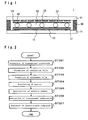
- Fig. 1 is a cross sectional view schematically showing an example of the construction of a liquid crystal optical device according to an embodiment of the present invention.
- a liquid crystal optical device 1 according to an embodiment of the present invention comprises a first transparent substrate 11, a first transparent electrode 12, a first insulation film 13, a first alignment film 14, a second transparent substrate 21, a second transparent electrode 22, a second insulation film 23, a second alignment film 24, a sealing member 30, a spacer 40 and a composite layer 50.
- the liquid crystal optical device 1 has a construction in which the first transparent substrate 11 and the second transparent substrate 21 are opposed to each other and the first and second transparent substrates 11, 21 sandwich the composite layer 50 of liquid crystal/cured material.
- the first and second transparent substrates 11, 21 are each an insulative substrate, and for example, it is a glass substrate, a resin substrate or a resin film substrate made of e.g. polycarbonate or an acrylic resin.
- the first and second transparent substrates 11, 21 are employed, but both of these substrates are not necessarily transparent, and it is sufficient that only one substrate is transparent.
- these insulative substrates may be a flat plate, or it may be entirely or partially curved.
- the thickness of the insulative substrates may be appropriately selected, and usually, it is preferably from 0.4 to 10 mm.
- first transparent electrodes 12 are formed in a stripe shape.
- second transparent electrodes 22 are formed in a stripe shape.
- the plurality of second transparent electrodes 22 are formed so as to cross substantially perpendicularly to the plurality of first transparent electrodes 12.
- the first and the second transparent electrodes 12, 22 are each made of e.g. ITO (Indium Tin Oxide).
- Either one of the first and the second transparent electrodes 12, 22 may be reflective electrodes of e.g. Al or dielectric multilayer film.
- shape of electrode is not limited to a perpendicular stripe shape, but the electrode may cover entire substrate surface or it may have a shape capable of displaying a specific mark or a character.
- the first and the second insulation films 13, 23 are formed so as to cover the first and the second transparent electrodes 12, 22, respectively.
- the first and the second insulation films 13, 23 are provided for the purpose of improving electric insulation, and they are made of a metal oxide such as SiO 2 , TiO 2 or Al 2 O 3 or other insulative materials.
- the first and the second insulation films 13, 23 are not essential.
- the first and the second alignment films 14, 24 are formed respectively.
- the alignment films 14, 24 are formed so as to contact with a liquid crystal in the composite layer 50 to align the liquid crystal in a predetermined direction.
- at least one of the alignment films formed on the transparent substrates 11, 21, preferably aligns the liquid crystal vertically to the inner faces of the transparent substrates 11, 21.
- the alignment film has a pretilt angle of preferably at least 60°, more preferably at least 80°, particularly preferably at least 85°.
- the sealing member 30 is formed between the first and second transparent substrates 11, 21 and along the periphery of the first and second transparent substrates 11, 21.
- the first and second transparent substrates 11, 21 are joined by means of the sealing member.
- a UV curable resin or a thermosetting resin is employed for the material of the sealing member 30, e.g. a UV curable resin or a thermosetting resin is employed.
- the distance between the inner faces of the first and second transparent substrates, 11, 21, that is, the thickness of the composite layer 50 (cell gap) is constant, and the height of the sealing member 30 is equal to the distance between inner faces of the first and second transparent substrates 11, 21.
- the liquid crystal optical device 1 of Fig. 1 has a flat shape, but the liquid crystal optical device of the present invention does not necessarily have a flat shape, but it may be partially or entirely curved depending on its application. Namely, it may have a three-dimensional shape. However, also in this case, the distance between inner faces of the first and second transparent substrate 11, 21, that is, the thickness of the composite layer 50 (cell gasp) is constant.
- the spacer 40 is uniformly spread in a space enclosed by the first and second transparent substrates 11, 21 and the sealing member 30.
- the spacer 40 controls cell gap.
- the cell gap that is the diameter of the spacer 40, is preferably from 2 to 50 ⁇ m, more preferably from 4 to 30 ⁇ m.
- the spacer 40 is a hard material such as glass particles, silica particles or crosslinked acryl particles.
- the spacer 40 is not necessarily spherical particles but it may be a rib-shaped spacer formed on one of the substrates.
- the composite layer 50 is sealed in a space (hereinafter it may be referred to as cell space) enclosed by the first and second transparent substrates 11, 21 and the sealing member 30.
- the composite layer 50 is made of a liquid crystal/cured material composite obtained by polymerizing and curing a curable compound in the liquid crystal composition of the present invention in a state that the liquid crystal composition is filled in a cell space and the liquid crystal is aligned.
- the content of the curable compound in the liquid crystal composition (this substantially equals to the content of the cured material of the curable compound contained in the liquid crystal/cured material composite) is preferably from 0.1 to 20 mass%.
- the liquid crystal phase can not be divided into domain structures each having more effective shape, and it is not possible to obtain a desired transparent-scattering characteristics.
- the haze value in transparent state increases.
- the content of the curable compound in the liquid crystal composition is more preferably from 0.5 to 10 mass%, since in this composition, it becomes possible to increase scattering intensity in scattering state of the liquid crystal/cured material composite, and to decrease a voltage at which transparent-scattering state is switched.
- the total amount of curable composition is preferably at most 20 mass%, particularly preferably at most 15 mass%.
- the content of curable compound in the liquid crystal composition is preferably from 0.1 to 20 mass% based on the liquid crystal composition, and it is preferably appropriately selected from a range of from 0.1 to 20 mass% depending on HTP (Helical Twisting Power) of the curable compound that is an optically active material.
- HTP Helical Twisting Power
- the curable compound being an optically active material has high HTP, only a small amount of the compound is required to be added to a chiral nematic liquid crystal being a mixture of nematic liquid crystal and a non-curable optically active material, to prepare a liquid crystal composition that as a whole shows a nematic phase.
- the most preferred content of the curable compound in the liquid crystal composition is from 0.5 to 5 mass%.
- the content is preferably from 0.5 to 10 mass% as described above.
- the content of non-curable optically active material in the liquid crystal composition is determined depending on HTP of the non-curable optically active material. Namely, when the non-curable optically active material has high HTP, the amount of non-curable optically active material for obtaining a desired pitch in a liquid crystal (a liquid crystal showing chiral nematic phase) in the liquid crystal/curable material composite, may be small.
- the content of the optically active material in the liquid crystal composition is preferably from 0.5 to 10 mass%, particularly preferably from 1 to 5 mass%.
- the liquid crystal composition of the present invention is a liquid crystal composition containing at least two types of optically active materials showing different optical rotatory directions and a nematic liquid crystal, and the liquid crystal composition as a whole shows nematic phase.
- the optical rotatory directions means dextro-rotatory and levo-rotatory, and "having different optical rotatory directions" means when one type of the material shows dextro-rotatory, the other material shows levo-rotatory.
- the nematic liquid crystal two or more types of nematic liquid crystals may be combined for use.
- the nematic liquid crystal changes into a chiral nematic liquid crystal with phase transition (it is also referred to as cholesteric liquid crystal) having a helical structure.
- optically active materials having different optical rotatories specifically, a chiral agent of dextro-rotatory and a chiral agent of levo-rotatory are added to a nematic liquid crystal to substantially maximize p to make the liquid crystal composition as a whole show a nematic phase.
- substantially maximize p means that, to be described later, p ⁇ d is satisfied provided that a cell gap is d.
- liquid crystal alignment in one direction can be realized by using an alignment film.
- vertical alignment film showing high pretilt angle it becomes easily possible to uniformly align a liquid crystal composition vertically to a substrate provided with a transparent electrode.
- a nematic phase means a state that provided that a twist angle of the liquid crystal between the first transparent substrate 11 and the second transparent substrate 21 is ⁇ , ⁇ 360° is satisfied, and it is preferred that ⁇ 180° is satisfied.
- a nematic phase means that the helical pitch satisfies p ⁇ d, and it is preferred that p ⁇ 2d.
- ⁇ >360°, that is p ⁇ d is satisfied, the nematic liquid crystal becomes close to the state of chiral nematic liquid crystal, and it becomes difficult to achieve uniform liquid crystal alignment in one direction by an alignment film.
- the twist angle of a nematic liquid crystal can be measured, for example, by sandwiching the liquid crystal composition between a pair of transparent substrates at least one of whose inner face is provided with an alignment film subjected to a rubbing treatment and showing a pretilt angle of at most 10°, and observing transmitted light by a polarizing microscopic observation while a polarizer is rotated. Further, the twist angle can be obtained by sandwiching the liquid crystal composition in a wedge-shaped cell and observing the distance between disclination lines.
- one of the optically active materials is a non-curable compound
- the other one of the optically active materials is a curable compound.
- the nematic liquid crystal changes into a chiral nematic liquid crystal with phase transition in a process of curing the curable compound by the effect of non-curable chiral agent remained.
- the non-curable chiral agent S-811, S-1011 or S-2011 manufactured by Merck & Co., Inc. may, for example, be mentioned. These chiral agents show levo-rotatory.
- a curable chiral agent contained at the same time is preferably an optical rotatory compound of dextro-rotatory such as Paliocolor LC 756 manufactured by BASF Corporation.
- non-curable chiral agent of dextro-rotatory and a curable chiral agent that is a levo-rotatory curable compound it is possible to provide a dextro-rotatory compound with relatively low cost by preparing the optical rotatory compound from an optical rotatory material present in natural world.
- the non-curable chiral agent one of levo-rotatory and one of dextro-rotatory may be used in combination, and in the same manner, for the curable chiral agent, one of levo-rotatory and one of dextro-rotatory may be used in combination.
- the effect of the present invention can be exhibited regardless of the combination of levo-rotatory and dextro-rotatory.
- a liquid crystal obtained by curing the curable compound in the liquid crystal composition of the present invention is considered to be a chiral nematic liquid crystal having a liquid crystal physical properties substantially equal to those of a mixture that is the remainder of the liquid crystal composition of the present invention other than the curable compound (including the curable compound other than the curable chiral agent), except in the influence of the cured material. Accordingly, the mixture is prepared so as to satisfy liquid crystal properties of chiral nematic liquid crystal required for the liquid crystal/cured material composite.
- the degree of optical rotatory and the amount of the curable chiral agent to be added to the mixture need to be ones capable of canceling chiral nematic properties of the mixture and converting them to nematic properties. In this requirement, the degree of optical rotatory of the curable chiral agent or its amount in the liquid crystal composition are not restricted by the degree of optical rotatory (in the opposite direction) of the non-curable chiral agent or its amount in the liquid crystal composition.
- the effect of the present invention can be exhibited in both of the cases where the dielectric anisotropy ( ⁇ ) of the liquid crystal composition is positive and where it is negative, and the effect can be exhibited in cases where the pretilt angle of the alignment film provided on an inner face of a substrate is at most 10° and where it is at least 60°. Further, a rubbing treatment may be applied to the alignment film.
- the chiral agent having curability contained in the liquid crystal composition is cured, a cured material produced by the curing reaction can efficiently divide chiral nematic phase produced in the process of curing reaction into a plurality of domains.
- a liquid crystal optical device showing a scattering state at a time of no voltage application and a transparent state at a time of voltage application can be extremely easily obtained from the liquid crystal composition of the present invention.
- the plurality of domains divided by the cured material are assumed to have different average refractive indexes, and incident light into the liquid crystal optical device is efficiently scattered by the plurality of liquid crystal domains having different average refractive indexes.
- liquid crystal composition of the present invention differently from PSCT described in Patent Document 5, it is not necessary to apply a voltage at a time of curing the liquid crystal composition in the process of forming a liquid crystal/cured material composite, and it is sufficient that the curable composition is cured in a non-voltage application state. Namely, when the curable compound is a photocurable compound, a liquid crystal optical device can be obtained on only by light exposure.
- liquid crystal/cured material composite obtainable from the liquid crystal composition of the present invention, since the content of cured material is low, even in a case of forming a liquid crystal optical device of large area, its haze value in transparent state is small and transparency is good on the angle of observing the device.
- the polarity of the dielectric anisotropy may be any one of positive or negative, but in order to reduce driving voltage, the dielectric anisotropy is preferably high. Further, in order to improve transparent-scattering contrast by increasing scattering intensity, it is preferred to increase the refractive index anisotropy ( ⁇ n) of the liquid crystal composition. On the other hand, if the dielectric anisotropy is too high, the electric insulation performance (specific resistance value) may decrease. Further, if the refractive index anisotropy is too high, the durability against UV light may decrease.
- a curable compound that is not optically active material may be contained.
- a liquid crystal showing positive dielectric anisotropy contains a curable compound having no mesogenic structure, it is possible to stabilize scattering state of liquid crystal phase obtained, and it is possible to provide a liquid crystal device showing uniform property even it has a large area.
- a curable compound may, for example, be alkyl acrylate, alkyl diacrylate, polyether acrylate, polyether diacrylate or a polyether type urethane acrylate.
- the curable compound that is not an optically active compound may further be a curable compound having a mesogenic structure.
- Such a curable compound having a mesogenic structure may, for example, be the following compounds (curable compounds represented by the following formulae (2) or (4) described in Patent Document 2).
- the total amount of curable compound (the amount including a curable compound that is an optically active compound) in the liquid crystal composition of the present invention is preferably at most 20 mass%, particularly preferably at most 10 mass% based on the total amount of liquid crystal composition. Further, as described above, in a case of employing a curable compound having high HTP (ranging from about 30 to 60) as the curable compound that is an optically active material, the total amount of the curable compound is preferably at most 5 mass% based on the total amount of liquid crystal composition.
- the alignment state of the liquid crystal composition having a nematic phase in non-cured state may be fixed to cause reduction of the contrast between on/off of voltage application.
- the total amount of the curable compound in the liquid crystal composition of the present invention is preferably at most 10 mass%, particularly preferably at most 5 mass% based on the total amount of liquid crystal composition.
- the liquid crystal composition in a case of employing a liquid crystal composition having negative dielectric anisotropy, in order to increase contrast between transparent and scattering, it is preferred to use an alignment film showing high pretilt angle and align the liquid crystal vertically to substrates with electrodes and to cure the curable composition in that state to fix the alignment state.
- the liquid crystal composition preferably contains a predetermined amount of the curable compound having a mesogenic structure.
- the amount of curable compound having a mesogenic structure is preferably from 3 to 18 mass%, particularly preferably from 5 to 14 mass% based on the total amount of liquid crystal composition.
- the total amount of the curable compound is preferably at most 20 mass%, particularly preferably at most 15 mass% based on the total amount of liquid crystal composition.
- a curing agent for initiating curing of the curable compound or a curing promoting agent (such as curing catalyst) for promoting curing may be contained. Particularly, it is preferred to employ a curing agent for initiating curing reaction.
- the curable compound is a polymerizable compound, it is preferred to employ a polymerization initiator.
- a common photopolymerization initiator such as that of benzoin ether type, acetophenone type or phosphine oxide type may be employed.
- its amount is preferably at most 5 mass%, particularly preferably at most 3 mass% based on the total amount of curable compound in the liquid crystal composition.
- various types of compounds may be added for the purpose of improving contrast or stability.
- various types of anisotropic dyes such as those of anthraquinone type, stearyl type, azomethine type or azo type may be employed.
- the anisotropic dyes are basically preferably soluble to the liquid crystal compound and insoluble to the curable compound.
- addition of e.g. an antioxidant, a UV-absorber or various types of plasticizer is preferred for the purpose of improving stability or durability.
- the total amount is preferably at most 20 mass%, particularly preferably at most 10 mass% based on the total amount of liquid crystal composition.
- the liquid crystal optical device 1 obtainable by aligning the liquid crystal composition having positive dielectric anisotropy vertically to substrates with electrodes and curing the curable compound.
- the liquid crystal having positive dielectric anisotropy is aligned vertically by an electric field between the electrodes, and the composite layer 50 becomes to be in transparent state.
- no voltage is applied between the first and second transparent electrodes 12, 22, as described above, since the chiral nematic liquid crystal produced in the process of curing reaction is randomly aligned between the electrodes, the composite layer 50 is presumed to be in scattering state.
- a liquid crystal optical device 1 obtainable by aligning the liquid crystal composition having negative dielectric anisotropy vertically to substrates with electrodes and curing the curable compound, may also be configured to be a liquid crystal optical device showing a scattering state at a time of voltage application and a transparent state at a time of no-voltage application.
- FIG. 2 is a view showing an example of production flow of a liquid crystal optical device according to an embodiment of the present invention. As shown in Fig. 2 , this production flow is constituted by 7 steps that are ST201 to ST207.
- transparent electrode films for forming second transparent electrodes 12, 22 are formed by e.g. a sputtering method or a vacuum vapor deposition method (ST201).
- the transparent electrode films are preferably ITO as described above.
- the transparent electrode films are each patterned into a desired character or pattern shape by a photolithography method, to form the first and second transparent electrodes 12, 22.
- the first and second insulation films 13, 23 are formed so as to cover the first and second transparent electrodes 12, 22 respectively by e.g. a solgel method, a sputtering method or a vacuum vapor deposition method (ST202).
- first and second alignment films 14, 24 respectively are formed (ST203).
- the first and second alignment films 14, 24 are, in order to align a liquid crystal composition showing a nematic phase in a predetermined direction between a pair of substrates with electrodes, formed so as to contact with the liquid crystal.
- at least one of the alignment films 14, 24 formed on the transparent substrates 11, 21 respectively is formed so as to align the liquid crystal vertically to the inner faces of the transparent substrates 11, 21.
- a sealing member 30 is applied along the periphery of the first or second transparent substrate 11 or 21 (ST205).
- the sealing member 30 e.g. a UV-curable resin or a thermosetting resin may be employed.
- the sealing member 30 may contain a spacer.
- the first and second transparent substrates 11, 21 are laminated to form a cell, and the cell is filled with a liquid crystal composition (ST206).
- a liquid crystal composition in this step, one of two seal-broken portions provided on the sealing member is immersed in the liquid crystal composition and suction is made through the other one of the seal-broken portions (suction method).
- a seal-broken portion of a cell having a sealing member provided with at least one seal-broken portion is immersed in a liquid crystal composition put in a container in vacuum, followed by returning the environmental pressure to the atmospheric pressure, to thereby fill inside the cell with the liquid crystal composition by the pressure difference between inner pressure of the cell and the atmospheric pressure (vacuum injection method).
- ODF one-drop-fill
- liquid crystal drop method vacuum drop method
- a predetermined amount of liquid crystal composition may be dropped, and under a low pressure, the first and the second transparent substrates 11, 21 are laminated with a sealing member 30 interposed therebetween.
- This ODF method requires a vacuum equipment, but.it can fill the liquid crystal composition in shorter time as compared with the suction method or the vacuum injection method, and the ODF method is effective for producing a large-sized liquid crystal optical device.
- the liquid crystal composition is sandwiched between inner faces of transparent substrates by the above methods. Since the liquid crystal composition shows a nematic phase in a state that the liquid crystal composition is sandwiched between inner faces of the transparent substrates, it is easily possible to align the liquid crystal in one direction by an alignment film.
- the step of laminating the first and second transparent substrates 11, 21 with the liquid crystal composition sandwiched therebetween may employ a method other than the above.
- a curable compound in the liquid crystal composition is cured (ST207).
- the curable compound in a state that the liquid crystal composition is sandwiched between inner faces of the transparent substrates and that the liquid crystal is aligned, the curable compound is cured. Since the liquid crystal is aligned in one direction before the compound is cured, the curable compound can be cured in a state that no voltage is applied between electrodes.
- the curable compound is a photocurable compound
- the compound is cured by exposing it by using a UV light source. By the exposure, the photocurable compound is cured to form a liquid crystal/cured material composite layer 50.
- the sealing member can be cured at the same time.
- curing of the sealing member needs to be carried out separately.
- Haze values were measured by using a direct read haze computer manufactured by Suga Test Instruments Co., Ltd.
- a levo-rotatory optically active material S-1011 manufactured by Merck & Co., Inc., HTP in the nematic liquid crystal is 38
- a chiral nematic liquid crystal having a helical pitch of about 0.82 ⁇ m.
- a dextro-rotatory optically active material (Paliocolor LC756 manufactured by BASF Corporation, HTP in the nematic liquid crystal is 56) was added to form again a nematic liquid crystal having a helical pitch of 18 ⁇ m.
- the above dextro-rotatory optically active material is a photocurable compound, and its content in the liquid crystal composition is 2.0 mass%.
- a photopolymerization initiator (benzoin isopropyl ether) is added in an amount of about 1 mass% based on the photocurable compound contained in the liquid crystal composition, to obtain a liquid crystal composition (liquid crystal composition A) according to the present invention.
- the liquid crystal composition A in order to measure the twist angle when the cell gap is 6 ⁇ m, the liquid crystal composition A was sandwiched between a pair of glass substrates each having an inner face provided with a polyimide thin film showing a pretilt angle of at most 10° as an alignment film, together with a slight amount of a spherical spacer having a diameter of 6 ⁇ m.
- a rubbing treatment as one side of those polyimide thin films, one subjected to a rubbing treatment was employed.
- the glass substrates sandwiching the liquid crystal composition A was observed by using a polarizing optical microscope, and as a result, the twist angle of the liquid crystal composition A was about 120°.
- a pair of glass substrates each having an inner face provided with an ITO thin film (indium tin oxide) as a transparent electrode are prepared, and on the ITO electrode, a metal oxide thin film (MIC-55 manufactured by SEIMI CHEMICAL CO., LTD.) of SiO 2 -TiO 2 type of about 50 nm thick was formed as an insulation layer. Further, on the insulation layer, an alignment film made of polyimide thin film having a pretilt angle of about 90° is formed.
- the pair of glass substrates was positioned so as to oppose to each other via a spacer that comprises resin beads of 6 ⁇ m in diameter, and they were sealed together with an epoxy resin other than a hole for injecting the liquid crystal composition, to prepare a cell.
- the above liquid crystal composition A is injected at a room temperature by a vacuum injection method, and the injection hole was sealed with a room-temperature curable sealing member. After the injection hole was sealed, the cell was observed, and as a result, the cell showed a transparent state having little haze. Then, the cell was exposed to UV-rays incident from glass substrate surfaces on both sides, that has a center wavelength of 365 nm and an intensity of 30 W/m 2 , at a room temperature for 10 minutes to cure the curable compound to thereby obtain a liquid crystal optical device.
- the liquid crystal optical device After the exposure of UV rays, the liquid crystal optical device showed an opaque state in white. Next, when a rectangular wave voltage of 200 Hz and 30 V was applied between the pair of ITO electrodes, and as a result, the liquid crystal optical device became transparent. Namely, a liquid crystal optical device was obtained, which showed a transparent state at a time of voltage application and a scattering state at a time of no-voltage application. In the transparent state, the haze value was at most 2% and its transparency was good. Further, the device of transparent state was observed in a state that observing direction was tilted from the direction perpendicular to the glass substrate, and as a result, increase of haze was hardly observed. By a Schlieren optical system of light collection angle of 5°, the contrast between transparent state and opaque state in white of this device was measured at a room temperature, and as a result, it was 25.
- liquid crystal composition A of the present invention differs from PSCT described in Patent Document 5, there is no need of applying voltage to the liquid crystal composition in a process of forming a liquid crystal optical device, and it is sufficient that a chiral agent having curability is cured.
- a chiral agent having curability is cured to divide a liquid crystal into a plurality of domains, whereby the liquid crystal changes from nematic phase to chiral nematic phase. Accordingly, a liquid crystal optical device can be extremely easily obtained, which shows a transparent state at a time of voltage application and a scattering state at a time of no-voltage application.
- liquid crystal optical device according to Example 1 since the content of cured material is low, haze value in transparent state is small, and its transparency is good regardless of angle of observing the device. Further, its contrast between transparent state and opaque state in white is also high.
- a liquid crystal optical device was produced in the same manner as Example 1 except that instead of the alignment film employed in Example 1, an alignment film having a pretilt angle of at most 10° on a face in contact with the liquid crystal composition A and subjected to a rubbing treatment was employed.
- the glass substrates were positioned so as to oppose to each other so that rubbing directions of their alignment films are perpendicular to each other.
- the liquid crystal device after it was exposed to UV-rays to cure the curable compound, showed an opaque state in white.
- a rectangular voltage of 200 Hz and 60 V was applied between the pair of ITO electrodes, and as a result, the liquid crystal optical device became transparent.
- a liquid crystal optical device was obtained, which showed a transparent state at a time of voltage application and a scattering state at a time of no-voltage application.
- the haze value in the transparent state was 4%.
- the device of transparent state was observed in a state that observation direction is tilted from a direction perpendicular to glass substrate, and as a result, slight increase of haze was observed, but the transparency was still good.
- a Schlieren optical system having a light collection angle of 5°, the contrast between transparent state and scattering state of this device was observed at a room temperature, and as a result, it was 12.
- liquid crystal composition A according to the present invention By employing the liquid crystal composition A according to the present invention, even in a case of employing a horizontal alignment film, by applying a rubbing treatment, in the same manner as the above Example 1, a liquid crystal device can be easily obtained, which shows a transparent state at a time of voltage application and a scattering state at a time of no-voltage application.
- the optical characteristics of the liquid crystal optical device according to Example 2 are, as compared with the above Example 1, generally slightly poor but still good.
- a levo-rotatory optically active material (HTP becomes about 24 when it is dissolved in the above nematic liquid crystal at a concentration of 10 mass%) in an amount of 3.5 mass% was added based on the amount of liquid crystal composition, to prepare a chiral nematic liquid crystal having a helical pitch of about 1.2 ⁇ m.
- a dextro-rotatory optically active material (Paliocolor LC756 manufactured by BASF Corporation, HTP in the nematic liquid crystal is 55) having curability was added, to make the liquid crystal again to a nematic liquid crystal having a helical pitch of at least 40 ⁇ m.
- the content of the dextro-rotatory optically active material in the liquid crystal composition is 1.8 mass%.
- a photopolymerization initiator (benzoin isopropyl ether) in an amount of about 1 mass% based on the photocurable compound contained in the liquid crystal composition was added, to obtain a liquid crystal composition (liquid crystal composition B).
- the liquid crystal composition B was sandwiched between a pair of glass substrates each provided with a polyimide film having a pretilt angle of at most 10° as an alignment film together with a slight amount of spherical spacer having a diameter of 10 ⁇ m.
- a polyimide film having a pretilt angle of at most 10° as an alignment film together with a slight amount of spherical spacer having a diameter of 10 ⁇ m.
- one side of the polyimide thin films one subjected to rubbing treatment was employed. Glass substrates sandwiching the liquid crystal composition B was observed by a polarizing microscope, and as a result, the twist angle of the liquid crystal composition B was at most 90°.
- a cell having a polyimide alignment film showing a pretilt angle of about 90° formed on a substrate surface that contact with the liquid crystal composition B was prepared in the same manner as Example 1 except that spacers of 10 ⁇ m in diameter was provided between transparent electrodes, and the liquid crystal composition B was injected into the cell by a vacuum injection method, and an injection hole was sealed.
- the cell showed a uniform transparent state with low haze.
- the cell was exposed to UV rays incident from both substrate surfaces in the manner as Example 1, to obtain a liquid crystal optical device.
- the liquid crystal optical device After the exposure of UV rays, the liquid crystal optical device showed an opaque state in white. Next, between the pair of ITO electrodes, a rectangular wave voltage of 200 Hz and 40 V was applied, and as a result, the liquid crystal optical device became transparent. The haze value in the transparent state was at most 2%. Further, the device of transparent state was observed in a direction tilted from a direction perpendicular to the glass substrate, and as a result, increase of haze was hardly observed. By using a Schlieren optical system having light collection angle of 5°, the contrast between transparent state and scattering state of the device was measured at a room temperature, and as a result, it was 8.
- liquid crystal optical device showing a transparent state at a time of voltage application and a scattering state at a time of no-voltage application can be obtained extremely easily. Further, by employing a vertical alignment film, a rubbing treatment can be omitted. Further, the optical characteristics of the liquid crystal optical device of Example 3 are good although the contrast is inferior to that of the liquid crystal optical device of Example 1.
- curable compound P represented by the following chemical formula (1) that is not an optically active material, was added so that its content becomes 1.7 mass% based on the total composition including (1).
- the curable compound P is a curable compound having no mesogenic structure in its molecule. Further, a photopolymerization initiator (benzoin isopropyl ether) in an amount of about 1 mass% based on the curable compound P was further added to prepare a liquid crystal composition (liquid crystal composition C). Since the curable compound P is not an optically active material, the helical pitch of the liquid crystal composition C is not different from the helical pitch of the liquid crystal composition B.
- a photopolymerization initiator benzoin isopropyl ether
- a cell having a polyimide alignment film showing a pretilt angle of about 90° formed on a substrate surface that contact with the liquid crystal composition C was prepared in the same manner as Example 1 except that a spacer of spherical beads of 10 ⁇ m in diameter was provided between transparent electrodes, and the liquid crystal composition C was injected into the cell by a vacuum injection method, and an injection hole was sealed.
- the cell showed a transparent state with low haze.
- the cell was exposed to UV rays incident from both substrate surfaces in the same manner as Example 1 to obtain a liquid crystal optical device.
- the liquid crystal optical device After the exposure of UV rays, the liquid crystal optical device showed an opaque state in white. Next, a rectangular wave voltage of 200 Hz and 40 V was applied between the pair of ITO electrodes, and as a result, the liquid crystal optical device became transparent. The haze value in the transparent state was at most 2%. When the device in the transparent state was observed in a direction tilted from a direction perpendicular to the glass substrate, the haze was low and the device showed a good transparency. Further, the contrast between the transparent state and the scattering state of the device was measured by using a Schlieren optical system having a light collection angle of 5° at a room temperature, and as a result, it was 15.
- liquid crystal optical device showing a transparent state at a time of voltage application and a scattering state at a time of non-voltage application can be easily obtained. Further, by employing a vertical alignment film, it is possible to omit rubbing treatment. Further, the optical characteristics of the liquid crystal optical device of Example 4 is better than the optical characteristics of the liquid crystal optical device of Example 2 employing the same nematic liquid crystal, since the device of Example 2 contains the curable compound P and shows better contrast.
- a levo-rotatory optically active material (its HTP is about 27 when it is dissolved in the nematic liquid crystal at a concentration of 10 mass%) was added so that its content becomes 3.1 mass% based on the liquid crystal composition, to prepare a chiral nematic liquid crystal having a helical pitch of about 1.2 ⁇ m.
- a dextro-rotatory optically active material (Paliocolor LC756 manufactured by BASF Corporation) having curability was added to produce again a nematic liquid crystal having a helical pitch of about 20 ⁇ m.
- the content of the dextro-rotatory optically active material in the liquid crystal composition is 1.5 mass%.
- a photopolymerization initiator (benzoin isopropyl ether) was added to the liquid crystal composition so that the content became about 1 mass% based on the photocurable compound contained in the liquid crystal composition, to obtain a liquid crystal composition (liquid crystal composition D).
- the liquid crystal composition D in order to measure the twist angle when the cell gap is 8 ⁇ m, the liquid crystal composition D was sandwiched between a pair of glass substrates whose inner faces are provided with a polyimide thin film as an alignment film showing a pretilt angle of at most 10°, together with a slight amount of spherical spacer of 8 ⁇ m in diameter.
- a polyimide thin film as an alignment film showing a pretilt angle of at most 10°, together with a slight amount of spherical spacer of 8 ⁇ m in diameter.
- the polyimide thin film of one side one subjected to rubbing treatment was employed.
- the glass substrates sandwiching the liquid crystal composition D were observed by a polarizing microscope, and as a result, the twist angle of the liquid crystal composition D was about 140°.
- a cell provided with a polyimide alignment films showing a pretilt angle of about 90° formed on substrate surfaces in contact with the liquid crystal composition D was prepared in the same manner as Example 1 except that spherical beads of 8 ⁇ m in diameter as a spacer was provided between the transparent electrodes, and the liquid crystal composition D was injected into the cell by a vacuum injection method, and the injection hole was sealed.
- the cell showed a uniform transparent state with low haze.
- the cell was exposed to UV rays incident from both substrate surfaces in the same condition as those of Example 1 to obtain a liquid crystal optical device.
- the liquid crystal optical device After the UV exposure, the liquid crystal optical device showed an opaque state in white. Next, a rectangular wave voltage of 200 Hz and 30 V was applied between the pair of ITO electrodes, and as a result, the liquid crystal optical device became transparent. The haze value in the transparent state was at most 2%, and when the transmittance of the device for incident light in perpendicular direction to glass substrate was measured by a Schlieren optical system having light collection angle of 5°, the transmittance was 84% including reflections on the substrate surfaces and absorption of incident light in the transparent electrodes. Next, by using the same measurement system, the device was tilted by 45° to the incident light and measured the transmittance, and as a result, it hardly changed and it was 83%. By using the same measurement optical system, the contrast between the transparent state and scattering state of the device was measured at a room temperature, and as a result, it was 15.
- liquid crystal composition D of Example 5 a liquid crystal optical device showing a transparent state at a time of voltage application and a scattering state at a time of no-voltage application can be easily obtained. Further, by employing a vertical alignment film, rubbing treatment can be omitted. Further, the optical characteristics of the liquid crystal device of Example 5 are better than the optical characteristics of the liquid crystal device of Example 1 although the contrast is slightly inferior.
- a levo-rotatory optically active material (its HTP is about 23 when it is dissolved in the nematic liquid crystal at a concentration of 10 mass%) was added so that its content becomes 2.9 mass% based on the liquid crystal composition, to prepare a chiral nematic liquid crystal having a helical pitch of about 1.5 ⁇ m.
- a curable dextro-rotatory optically active material (Paliocolor LC756 manufactured by BASF Corporation, its HTP in the nematic liquid crystal is 44) was added to again prepare a nematic liquid crystal having a helical pitch of about 23 ⁇ m.
- the content of the dextro-rotatory optically active material in the liquid crystal composition is 1.5 mass%.
- a photopolymerization initiator (benzoin isopropyl ether) was added so that its content becomes about 1 mass% based on the photocurable compound contained in the liquid crystal composition, to obtain a liquid crystal composition (liquid crystal composition E).
- the liquid crystal composition E in order to measure the twist angle in a case where the cell gap is 6 ⁇ m, in the same manner as Example 1, the liquid crystal composition E was sandwiched between a pair of glass substrates having inner faces each provided with a polyimide thin film showing a pretilt angle of at most 10° as alignment films, together with a slight amount of spherical spacers of 6 ⁇ m in diameter. At this time, for the polyimide thin film of one side, one subjected to a rubbing treatment was employed. The glass substrates sandwiching the liquid crystal composition E were observed by a polarizing microscope, and as a result, the twist angle of the liquid crystal composition E was about 90°.
- a cell provided with polyimide alignment films having a pretilt angle of about 90° formed on substrate surfaces in contact with the liquid crystal composition E was prepared in the same manner as Example 1 except that the spherical beads of 6 ⁇ m in diameter as a spacer was provided between the transparent electrodes, and the liquid crystal composition E was injected into the cell by a vacuum injection method, and the injection hole was sealed.
- the cell showed a uniform transparent state with low haze.
- the cell was exposed to UV rays incident from both substrate surfaces to obtain a liquid crystal optical device.
- the liquid crystal optical device After the exposure of UV rays, the liquid crystal optical device showed a transparent state with slight opaqueness in white.
- a rectangular wave voltage of 200 Hz and 15 V was applied to the pair of ITO electrodes, and as a result, the transparency of the liquid crystal optical device slightly increased, and the transparency measured by a Schlieren optical system having light collection angle of 5° was 65%.
- a rectangular wave voltage of 200 Hz and 60 V was applied between the ITO electrodes, as a result, the device showed a scattering state, the transmittance by the same measurement system was 5%, and the contrast between the transparent state and scattering state was 13.
- An electrooptical device whose degree of scattering intensity increases by voltage application was obtained.
- HTP levo-rotatory optically active material
- a curable dextro-rotatory optically active material (Paliocolor LC756 manufactured by BASF Corporation, its HTP in the nematic liquid crystal is 50) was added, to again produce a nematic liquid crystal having a helical pitch of abut 23 ⁇ m.
- the content of the dextro-rotatory optically active material in the liquid crystal composition is 0.5 mass%.
- a curable compound (curable compound R) represented by the following chemical formula (2) that is not an optically active material was added so that its content becomes 10 mass% based on the total composition including (2).
- the curable compound R is a curable compound having a mesogenic structure in its molecule. Further, a photopolymerization initiator (benzoin isopropyl ether) in an amount of about 1 mass% based on the total curable compound contained was further added to prepare a liquid crystal composition (liquid crystal composition F). Since the curable compound R is not an optically active material, the liquid crystal composition F is also a nematic liquid crystal having a helical pitch of about 23 ⁇ m.
- the liquid crystal composition F in order to measure twist angle in a case where the cell gap is 10 ⁇ m, in the same manner as Example 1, the liquid crystal composition F was sandwiched between a pair of glass substrates having inner faces each provided with a polyimide thin film having a pretilt angle of at most 10° as an alignment film, together with a slight amount of spherical spacers of 10 ⁇ m in diameter. At this time, as one of the polyimide thin films, one subjected to a rubbing treatment was employed. When the glass substrates sandwiching the liquid crystal composition F were observed by a polarizing microscope, the twist angle of the liquid crystal composition F was about 160°.
- a cell provided with a polyimide alignment films having a pretilt angle of 90° formed on substrate surfaces in contact with the liquid crystal composition F was prepared in the same manner as Example 1 except that spherical beads of 10 ⁇ m in diameter as a spacer was provided between the transparent electrodes, and the liquid crystal composition F was injected into the cell by a vacuum injection method, and the injection hole was sealed.
- the cell showed a uniform transparent state with low haze.
- the cell was exposed to UV rays incident from both substrate surfaces in the same manner as Example 1 to obtain a liquid crystal optical device.
- the liquid crystal optical device After the UV exposure, the liquid crystal optical device showed a transparent state with a slight haze. Next, when a rectangular wave voltage of 200 Hz and 40 V was applied between the pair of ITO electrodes, the device showed a strong scattering state. The contrast between the transparent state and scattering state of the device was measured by using a Schlieren optical system having light collection angle of 5° at a room temperature, and as a result, it was 17. An electrooptical device whose degree of scattering intensity is increased by voltage application was obtained.
- Solid product was filtered out, and an organic layer was cleaned with an ion exchanged water of about pH 4, with a sodium bicarbonate water and with an ion-exchanged water in this order, to carry out an extraction operation.
- the organic layer was dried by magnesium sulfate anhydride, and filtered, and dichloromethane was removed by distillation by using a rotary evaporator.
- a white solid product obtained was further recrystallized in ethanol to obtain an objective compound.
- the amount obtained was 0.62 g, and the yield was 26%.
- a levo-rotatory optically active material S-1011 manufactured by Merck & Co. was added in an amount of 2.3 mass% based on the liquid crystal composition, to prepare a chiral nematic liquid crystal having a helical pitch of about 1.2 ⁇ m.
- the dextro-rotatory optically active material (curable compound 3, HTP in the nematic liquid crystal was 42) obtained in the Synthesis Example and represented by formula (3), was added to again produce a nematic liquid crystal having a helical pitch of at least about 40 ⁇ m.
- the dextro-rotatory optically active material is a photocurable compound, and the content in the liquid crystal composition is 1.9 mass%.
- a photopolymerization initiator (benzoin isopropyl ether) in an amount of abut 1 mass% based on the photocurable compound contained in the liquid crystal composition, was added, to obtain a liquid crystal composition (liquid crystal composition H) according to the present invention.
- the liquid crystal composition H in order to measure the twist angle when the cell gap is 10 ⁇ m, the liquid crystal composition H was sandwiched between a pair of glass substrates having inner surfaces each provided with a polyimide thin film showing a pretilt angle of at most 10° as alignment films, together with a slight amount of a spherical spacers having a diameter of 10 ⁇ m.
- a polyimide thin film on one of the inner surfaces one subjected to a rubbing treatment was employed.
- the twist angle of the liquid crystal composition H was at most 90°.
- a cell provided with polyimide alignment films showing a pretilt angle of about 90° formed on substrate surfaces that contact with the liquid crystal composition H was prepared in the same manner as Example 1 except that the diameter of the spacer was 10 ⁇ m, and the liquid crystal composition H was injected into the cell by a vacuum injection method, and the injection holes was sealed.
- the cell showed a uniform transparent state with low haze.
- the cell was exposed to UV rays incident from both substrate surfaces in the same manner as Example 1 to obtain a liquid crystal optical device.
- the liquid crystal optical device After the UV exposure, the liquid crystal optical device showed an opaque state in white. Next, a rectangular wave voltage of 200 Hz and 60 V was applied between the pair of ITO electrodes, and as a result, the liquid crystal optical device became transparent. Namely, a liquid crystal optical device was obtained which showed a transparent state at a time of voltage application and a scattering state at a time of no-voltage application. The haze value in the transparent state was at most 2%, and the transparency was good. Further, when the device was observed in a direction tilted from a direction perpendicular to the glass substrates, increase of haze was hardly observed. By using a Schlieren optical system having light collection angle of 5°, the contrast between the transparent state and scattering state of this device was observed at a room temperature, and as a result, it was 13. A device whose degree of scattering intensity increased by voltage application was obtained.
- liquid crystal compositions according to Examples 1 to 5 and 8 show positive dielectric anisotropy
- the liquid crystal compositions E and F according to Examples 6 and 7 show negative dielectric anisotropy.
- liquid crystal optical devices showing a scattering state at a time of voltage application and showing more transparent state at a time of no-voltage application can be easily obtained. Further, by employing a vertical alignment film, it is possible to omit rubbing treatment. Further, the liquid crystal optical devices according to Examples 6 and 7, show a relatively high contrast between transparent state and scattering state.
- composition G a photopolymerization initiator (benzoin isopropyl ether) in an amount of about 1 mass% based on the curable composition contained, was added and uniformly dissolved to obtain a composition (composition G). At a room temperature, the composition G became isotropic phase showing no liquid crystal state, and showed a uniform transparent state.
- a photopolymerization initiator benzoin isopropyl ether
- a cell provided with polyimide alignment films showing a pretilt angle of at most 10° formed on substrate surfaces that contact with the composition G was prepared in the same manner as Example 2 except that spherical beads of 8 ⁇ m in diameter as a spacer was provided between transparent electrodes, and the liquid crystal composition G was injected into the cell by a suction injection method, and the injection hole was sealed. In order to use the suction injection method, at least two holes were provided at the sealing portion. After the injection of composition G, the cell showed a uniform transparent state.
- the cell was subjected to UV rays having a central wavelength of 365 nm and an irradiation intensity of 10 W/m 2 incident from glass substrates on both sides, for three minutes to cure the liquid crystal composition G, to thereby obtain a liquid crystal optical device.
- the liquid crystal optical device After the UV exposure, the liquid crystal optical device showed an opaque state in white. Next, a rectangular wave voltage of 200 Hz and 40 V was applied between the pair of ITO electrodes, and as a result, the liquid crystal optical device became transparent. The haze value in the transparent state was at most 2%, and when the transparency of the device for incident light in a direction perpendicular to the glass substrates of the device was observed by using a Schlieren optical system having collection angle of 5°, the transparency was 84% including reflection on glass substrate surfaces and absorption in the transparent electrode layers. Next, the transmittance was measured in the same measurement system under the condition that the device was tilted by 45° to the incident light, and as a result, the transmittance was 72%.
- the liquid crystal device according to the present invention is suitable particularly for sunroofs of automobiles, and the device can be also used for other applications.
- it is applicable to windows (for automobiles (side windows, door glasses, rear quarters etc.), for architectures, for airplanes, for ships, for railroad vehicles etc.), skylights, partitions, materials for interior or exterior of architectures such as doors, sign boards, commercial advertising mediums, large-sized partition equipment, projection screens combined with projection type display devices, finders for cameras or digital cameras or the like.
- windows for automobiles (side windows, door glasses, rear quarters etc.), for architectures, for airplanes, for ships, for railroad vehicles etc.), skylights, partitions, materials for interior or exterior of architectures such as doors, sign boards, commercial advertising mediums, large-sized partition equipment, projection screens combined with projection type display devices, finders for cameras or digital cameras or the like.
- the device for a door of a refrigerator it is possible to recognize foods contained in the refrigerator without opening the door of refrigerator.
Landscapes
- Chemical & Material Sciences (AREA)
- Crystallography & Structural Chemistry (AREA)
- Engineering & Computer Science (AREA)
- Materials Engineering (AREA)
- Organic Chemistry (AREA)
- Physics & Mathematics (AREA)
- Nonlinear Science (AREA)
- Dispersion Chemistry (AREA)
- Mathematical Physics (AREA)
- General Physics & Mathematics (AREA)
- Optics & Photonics (AREA)
- Liquid Crystal (AREA)
- Liquid Crystal Substances (AREA)
Claims (14)
- Une composition à base de cristaux liquides contenant un cristal liquide nématique et au moins deux types de matériaux optiquement actifs ayant des sens de rotation optique différents, dans laquelle un des matériaux optiquement actifs ayant des sens de rotation optique différents est un composé non durcissable, l'autre des matériaux optiquement actifs est un composé durcissable, et la composition à base de cristaux liquides dans son ensemble présente une phase nématique.
- La composition à base de cristaux liquides selon la revendication 1, qui présente une phase nématique chirale lorsque le matériau optiquement actif qui est un composé durcissable n'est pas présent, et qui dans son ensemble présente une phase nématique lorsque la composition à base de cristaux liquides contient le matériau optiquement actif qui est un composé durcissable.
- La composition à base de cristaux liquides selon la revendication 1 ou 2, qui est une composition à base de cristaux liquides contenant par ailleurs un composé durcissable qui n'est pas un matériau optiquement actif.
- La composition à base de cristaux liquides selon l'une quelconque des revendications 1 à 3, dans laquelle la quantité totale du composé durcissable est de 0,1 à 20% en masse sur la base de la quantité totale de la composition à base de cristaux liquides.
- La composition à base de cristaux liquides selon l'une quelconque des revendications 1 à 4, qui présente un angle de torsion d'au plus 360° lorsqu'elle est intercalée entre une paire de substrats dont l'un au moins a une surface intérieure dotée d'un film d'alignement ayant un angle de préinclinaison d'au plus 10°.
- La composition à base de cristaux liquides selon l'une quelconque des revendications 1 à 5, qui a une anisotropie diélectrique positive.
- Un procédé de production d'une composition à base de cristaux liquides, qui comprend une étape consistant à ajouter à une composition contenant un cristal liquide nématique et au moins un type de premier matériau optiquement actif et présentant une phase nématique chirale, au moins un type de second matériau optiquement actif ayant un sens de rotation optique différent du sens de rotation optique du premier matériau optiquement actif, dans une quantité qui fait en sorte que la composition à base de cristaux liquides dans son ensemble présente une phase nématique ; dans lequel l'un du premier matériau optiquement actif et du second matériau optiquement actif est un composé durcissable, et l'autre est un composé non durcissable.
- Le procédé de production d'une composition à base de cristaux liquides selon la revendication 7, dans lequel le premier matériau optiquement actif est un composé non durcissable et le second matériau optiquement actif est un composé durcissable.
- Un élément optique à base de cristaux liquides comprenant une paire de substrats isolants dont l'un au moins est transparent, une électrode formée sur une face intérieure de chacun des substrats isolants, et un composite de cristal liquide et de matériau durci intercalé entre les faces intérieures des substrats isolants,
dans lequel le composite peut être obtenu en durcissant le composé durcissable dans la composition à base de cristaux liquides telle que définie dans l'une quelconque des revendications 1 à 6 dans un état où la composition à base de cristaux liquides est intercalée entre les faces intérieures des substrats isolants et où le cristal liquide est aligné. - L'élément optique à base de cristaux liquides selon la revendication 9, qui est obtenu en durcissant le composé durcissable dans un état où aucune tension n'est appliquée aux électrodes.
- L'élément optique à base de cristaux liquides selon la revendication 9 ou 10, dans lequel au moins un des substrats isolants est doté d'un film d'alignement ayant un angle de préinclinaison d'au moins 60°.
- Un procédé de production d'un élément optique à base de cristaux liquides ayant un composite de cristal liquide et de matériau durci, qui comprend une étape consistant à former une électrode sur chaque face intérieure d'une paire de substrats isolants dont l'un au moins est transparent, une étape consistant à laminer les substrats isolants de manière à ce qu'ils intercalent entre eux la composition à base de cristaux liquides telle que définie dans l'une quelconque des revendications 1 à 6 de sorte que les faces intérieures des substrats isolants respectifs soient opposées l'une à l'autre, et une étape consistant à durcir le composé durcissable dans la composition à base de cristaux liquides dans un état où la composition à base de cristaux liquides est intercalée entre les faces intérieures des substrats isolants et où le cristal liquide est aligné, pour former le composite.
- Le procédé de production d'un élément optique à base de cristaux liquides selon la revendication 12, dans lequel le durcissement du composé durcissable est réalisé dans un état où aucune tension n'est appliquée aux électrodes.
- Le procédé de production d'un élément optique à base de cristaux liquides selon la revendication 12 ou 13, qui comprend en outre une étape consistant à former sur au moins un des substrats isolants un film d'alignement ayant un angle de préinclinaison d'au moins 60°.
Applications Claiming Priority (2)
| Application Number | Priority Date | Filing Date | Title |
|---|---|---|---|
| JP2006176079 | 2006-06-27 | ||
| PCT/JP2007/062927 WO2008001817A1 (fr) | 2006-06-27 | 2007-06-27 | composition À CRISTAUX LIQUIDES, élément optique à cristaux liquides, et procédé de fabrication d'ÉLÉMENT OPTIQUE À CRISTAUX LIQUIDES |
Publications (3)
| Publication Number | Publication Date |
|---|---|
| EP2045309A1 EP2045309A1 (fr) | 2009-04-08 |
| EP2045309A4 EP2045309A4 (fr) | 2010-06-23 |
| EP2045309B1 true EP2045309B1 (fr) | 2011-09-28 |
Family
ID=38845582
Family Applications (1)
| Application Number | Title | Priority Date | Filing Date |
|---|---|---|---|
| EP07767727A Not-in-force EP2045309B1 (fr) | 2006-06-27 | 2007-06-27 | Composition à base de cristaux liquides, element optique à base de cristaux liquides, et procédé de fabrication d'élément optique à base de cristaux liquides |
Country Status (6)
| Country | Link |
|---|---|
| US (1) | US7864287B2 (fr) |
| EP (1) | EP2045309B1 (fr) |
| JP (2) | JP5242390B2 (fr) |
| CN (1) | CN101479363B (fr) |
| AT (1) | ATE526384T1 (fr) |
| WO (1) | WO2008001817A1 (fr) |
Families Citing this family (16)
| Publication number | Priority date | Publication date | Assignee | Title |
|---|---|---|---|---|
| EP2042915A4 (fr) * | 2006-07-14 | 2010-05-26 | Asahi Glass Co Ltd | Dispositif optique à cristaux liquides et procédé de fabrication de celui-ci |
| US8294850B2 (en) * | 2009-03-31 | 2012-10-23 | Apple Inc. | LCD panel having improved response |
| AR076936A1 (es) * | 2009-06-02 | 2011-07-20 | Vitae Pharmaceuticals Inc | Inhibidores de carbamato y urea de la 11 beta hidroxiesteroide deshidrogenasa 1 |
| PL2513251T3 (pl) | 2009-12-16 | 2015-10-30 | Basf Se | Środek ogniochronny |
| KR101854005B1 (ko) * | 2014-08-27 | 2018-05-02 | 주식회사 엘지화학 | 액정 조성물 |
| KR101854006B1 (ko) * | 2014-09-03 | 2018-05-02 | 주식회사 엘지화학 | 액정 조성물 |
| TW202244246A (zh) * | 2014-11-06 | 2022-11-16 | 公立大學法人兵庫縣立大學 | 光反應性液晶組成物,調光元件,調光元件之製造方法 |
| JP6808915B2 (ja) * | 2015-08-06 | 2021-01-06 | Agc株式会社 | 液晶組成物および液晶光学素子 |
| US11274252B2 (en) * | 2015-12-15 | 2022-03-15 | Merck Patent Gmbh | Mixed left/right chiral liquid crystal for improved switching speed and tunability for RF devices |
| EP3404474B1 (fr) * | 2016-07-27 | 2020-07-08 | LG Chem, Ltd. | Film à transmission variable, procédé de fabrication de celui-ci, et son utilisation |
| KR20230051625A (ko) * | 2016-12-22 | 2023-04-18 | 다이니폰 인사츠 가부시키가이샤 | 조광 부재, 조광 부재의 제조 방법, 조광체, 차량 |
| JP2019045185A (ja) * | 2017-08-30 | 2019-03-22 | Dic株式会社 | 帯電インジケータ |
| US20220107522A1 (en) * | 2019-01-22 | 2022-04-07 | Nitto Denko Corporation | Polymer networked liquid crystal smart window device and methods of making the same |
| CN113874469B (zh) * | 2019-05-15 | 2024-09-10 | 默克专利股份有限公司 | 制备基于液晶的切换元件的方法 |
| CN110850624A (zh) * | 2019-11-25 | 2020-02-28 | 南京华日触控显示科技有限公司 | 一种上下不同配向方式的胆甾相液晶显示屏及其方法 |
| JPWO2024070757A1 (fr) * | 2022-09-29 | 2024-04-04 |
Family Cites Families (32)
| Publication number | Priority date | Publication date | Assignee | Title |
|---|---|---|---|---|
| WO1985004262A1 (fr) | 1984-03-19 | 1985-09-26 | Kent State University | Materiau photomodulateur comprenant une dispersion de cristaux liquides dans une matrice de resine synthetique |
| DE3752026T2 (de) | 1986-12-23 | 1997-06-26 | Asahi Glass Co Ltd | Optische Flüssigkristall-Vorrichtung und Verfahren zu ihrer Herstellung. |
| US4818070A (en) | 1987-01-22 | 1989-04-04 | Asahi Glass Company Ltd. | Liquid crystal optical device using U.V.-cured polymer dispersions and process for its production |
| US6122021A (en) | 1988-10-04 | 2000-09-19 | Asahi Glass Company, Ltd. | Liquid crystal display element and a projection type liquid crystal display apparatus |
| US5150232A (en) | 1988-10-04 | 1992-09-22 | Asahi Glass Company Ltd. | Active matrix liquid crystal display element and projection type active matrix liquid crystal display device |
| JPH02272090A (ja) * | 1989-04-13 | 1990-11-06 | Canon Inc | 高分子液晶組成物および高分子液晶素子 |
| US5162934A (en) | 1989-07-31 | 1992-11-10 | Asahi Glass Company Ltd. | Method of manufacturing liquid crystal display element |
| US5200845A (en) | 1989-10-31 | 1993-04-06 | University Of Hawaii At Manoa | Color liquid crystal display consisting of polymer-dispersed chiral liquid crystal having negative dielectric anisotropy |
| DE69106966T2 (de) | 1990-07-26 | 1995-08-24 | Asahi Glass Co Ltd | Flüssigkristallanzeigeelement sowie Flüssigkristall-Projektionsanzeigevorrichtung mit einer aktiven Matrix. |
| US5216531A (en) | 1990-08-28 | 1993-06-01 | Asahi Glass Company Ltd. | Projection type active matrix polymer dispersed liquid crystal display apparatus with particles of liquid crystal material randomly oriented |
| DE69225738T2 (de) | 1991-03-27 | 1998-10-01 | Technology Co Ag | Flüssigkristallanzeigeelement und Projektionsanordnung unter Verwendung desselben |
| EP0509534B1 (fr) | 1991-04-17 | 1997-03-05 | AG-TECHNOLOGY Co., Ltd. | Elément optique à cristal liquide, élément d'affichage à cristal liquide et dispositif d'affichage par projection à cristal liquide utilisant cet élément |
| US6034753A (en) * | 1991-11-27 | 2000-03-07 | Reveo, Inc. | Circularly polarizing reflective material having super broad-band reflection and transmission characteristics and method of fabricating and using same in diverse applications |
| DE69229003T2 (de) | 1992-05-18 | 1999-10-21 | Kent State University, Kent | Flüssigkristalline, lichtmodulierende vorrichtung und material |
| DE69431941T2 (de) * | 1993-03-29 | 2003-04-30 | Seiko Epson Corp., Tokio/Tokyo | Anzeigevorrichtung und elektronischer apparat |
| JP2692673B2 (ja) * | 1996-03-25 | 1997-12-17 | 旭硝子株式会社 | 光シャッター装置 |
| JPH10195445A (ja) * | 1997-01-07 | 1998-07-28 | Matsushita Electric Ind Co Ltd | 液晶表示素子 |
| JP4352480B2 (ja) | 1998-10-20 | 2009-10-28 | 旭硝子株式会社 | 液晶光学素子およびその製造方法 |
| US6723393B1 (en) | 1998-10-20 | 2004-04-20 | Asahi Glass Company, Limited | Liquid crystal optical element and method for preparing the same |
| JP2000178557A (ja) * | 1998-12-14 | 2000-06-27 | Minolta Co Ltd | 液晶組成物及び液晶光変調素子 |
| JP4287599B2 (ja) * | 2000-06-27 | 2009-07-01 | 富士フイルム株式会社 | 光反応型光学活性化合物、光反応型カイラル剤、液晶組成物、液晶カラーフィルタ、光学フィルム、記録媒体、及び液晶の捻れ構造を変化させる方法 |
| JP4287598B2 (ja) * | 2000-06-27 | 2009-07-01 | 富士フイルム株式会社 | 光反応型カイラル剤、液晶組成物、液晶カラーフィルタ、光学フィルム、記録媒体、及び液晶の捻れ構造を変化させる方法 |
| JP2002179669A (ja) * | 2000-12-14 | 2002-06-26 | Fuji Photo Film Co Ltd | 光学活性化合物、光反応型キラル剤、液晶組成物、液晶の捻れ構造を変化させる方法、液晶の螺旋構造を固定化する方法、液晶カラーフィルタ、光学フィルム及び記録媒体 |
| JP4322418B2 (ja) * | 2000-12-14 | 2009-09-02 | 富士フイルム株式会社 | 光学活性化合物、光反応型キラル剤、液晶組成物、液晶の螺旋構造を変化させる方法、液晶の螺旋構造を固定化する方法、液晶カラーフィルタ、光学フィルム、及び記録媒体 |
| JP4137436B2 (ja) * | 2000-12-14 | 2008-08-20 | 富士フイルム株式会社 | 光学活性化合物、液晶組成物用光反応型キラル剤、液晶組成物、液晶の螺旋構造を変化させる方法、液晶の螺旋構造を固定化する方法、液晶カラーフィルター、光学フィルムおよび記録媒体 |
| US6674494B2 (en) | 2000-12-28 | 2004-01-06 | Optrex Corporation | Liquid crystal optical element and test method for its boundary layer |
| JP3933422B2 (ja) * | 2001-08-10 | 2007-06-20 | シャープ株式会社 | 反射膜および反射膜の製造方法 |
| JP2003082352A (ja) * | 2001-09-17 | 2003-03-19 | Fuji Photo Film Co Ltd | 液晶組成物、選択反射膜、及びその製造方法 |
| ATE420150T1 (de) * | 2001-09-25 | 2009-01-15 | Merck Patent Gmbh | Anisotroper polymerfilm |
| JP4207559B2 (ja) * | 2002-12-20 | 2009-01-14 | 富士ゼロックス株式会社 | 光変調媒体および光変調方法 |
| GB2420563B (en) * | 2003-08-26 | 2008-07-16 | Merck Patent Gmbh | Polymer film with twist pattern |
| JP4392339B2 (ja) | 2004-12-24 | 2009-12-24 | 住友ゴム工業株式会社 | 空気入りタイヤ |
-
2007
- 2007-06-27 JP JP2008522608A patent/JP5242390B2/ja not_active Expired - Fee Related
- 2007-06-27 AT AT07767727T patent/ATE526384T1/de not_active IP Right Cessation
- 2007-06-27 EP EP07767727A patent/EP2045309B1/fr not_active Not-in-force
- 2007-06-27 CN CN2007800246438A patent/CN101479363B/zh active Active
- 2007-06-27 WO PCT/JP2007/062927 patent/WO2008001817A1/fr not_active Ceased
-
2008
- 2008-12-29 US US12/344,610 patent/US7864287B2/en active Active
-
2013
- 2013-04-01 JP JP2013075836A patent/JP5761244B2/ja not_active Expired - Fee Related
Also Published As
| Publication number | Publication date |
|---|---|
| US7864287B2 (en) | 2011-01-04 |
| ATE526384T1 (de) | 2011-10-15 |
| JP5761244B2 (ja) | 2015-08-12 |
| EP2045309A4 (fr) | 2010-06-23 |
| JPWO2008001817A1 (ja) | 2009-11-26 |
| CN101479363A (zh) | 2009-07-08 |
| EP2045309A1 (fr) | 2009-04-08 |
| JP5242390B2 (ja) | 2013-07-24 |
| JP2013166950A (ja) | 2013-08-29 |
| US20090128770A1 (en) | 2009-05-21 |
| CN101479363B (zh) | 2012-09-05 |
| WO2008001817A1 (fr) | 2008-01-03 |
Similar Documents
| Publication | Publication Date | Title |
|---|---|---|
| US7864287B2 (en) | Liquid crystal composition, liquid crystal optical device, and method of producing liquid crystal optical device | |
| EP2042915A1 (fr) | Dispositif optique à cristaux liquides et procédé de fabrication de celui-ci | |
| EP2360229B1 (fr) | Milieu cristal liquide optiquement isotrope et élément optique correspondant | |
| KR0173803B1 (ko) | 액정표시소자 및 그의 제조방법 | |
| KR101066784B1 (ko) | 액정 표시 소자 | |
| CN1989444B (zh) | 包含图案化延迟膜的半透半反射式lcd | |
| US8409673B2 (en) | Chlorobenzene derivative, optically isotropic liquid crystal medium, and optical device | |
| US7459189B2 (en) | Liquid crystal optical element and process for its production | |
| WO2002042832A2 (fr) | Stratifie d"affichage a cristaux liquides et son procede de production | |
| WO2012043145A1 (fr) | Milieu à cristaux liquides optiquement isotrope et dispositif optique | |
| CN112987413A (zh) | 用于调节光透射的器件 | |
| JP4528645B2 (ja) | 液晶表示素子 | |
| JP2008310188A (ja) | 液晶光学素子 | |
| US5814378A (en) | Polymerizable compound and a liquid crystal display device using the same | |
| JP2010152258A (ja) | 液晶表示装置およびその製造方法 | |
| JP5560525B2 (ja) | 液晶組成物及び液晶組成物の製造方法、並びに、液晶素子及び液晶素子の製造方法 | |
| KR0162271B1 (ko) | 액정표시소자 및 그 제조방법 | |
| JPH0953074A (ja) | 液晶表示素子及び液晶表示素子の製造方法 | |
| JPH08190086A (ja) | 液晶表示素子及びこれを用いた表示装置 | |
| JP2000089216A (ja) | 液晶表示装置 | |
| JP2008191524A (ja) | 液晶光学素子 | |
| KR101892568B1 (ko) | 고분자 분산 액정 렌즈 | |
| JPH08134454A (ja) | 液晶表示素子及びこれを用いた表示装置 | |
| Lin et al. | P‐168: Reflective Type Polarizer‐Free Flexible Displays Using Dye‐Doped Nematic Liquid Crystal Gels | |
| Chien et al. | Smart materials for polymer-stabilized reflective cholesteric displays |
Legal Events
| Date | Code | Title | Description |
|---|---|---|---|
| PUAI | Public reference made under article 153(3) epc to a published international application that has entered the european phase |
Free format text: ORIGINAL CODE: 0009012 |
|
| 17P | Request for examination filed |
Effective date: 20090115 |
|
| AK | Designated contracting states |
Kind code of ref document: A1 Designated state(s): AT BE BG CH CY CZ DE DK EE ES FI FR GB GR HU IE IS IT LI LT LU LV MC MT NL PL PT RO SE SI SK TR |
|
| AX | Request for extension of the european patent |
Extension state: AL BA HR MK RS |
|
| A4 | Supplementary search report drawn up and despatched |
Effective date: 20100525 |
|
| RIC1 | Information provided on ipc code assigned before grant |
Ipc: C09K 19/54 20060101ALI20100518BHEP Ipc: C09K 19/38 20060101AFI20080314BHEP Ipc: C09K 19/58 20060101ALI20100518BHEP Ipc: G02F 1/13 20060101ALI20100518BHEP Ipc: G02F 1/1334 20060101ALI20100518BHEP |
|
| DAX | Request for extension of the european patent (deleted) | ||
| GRAP | Despatch of communication of intention to grant a patent |
Free format text: ORIGINAL CODE: EPIDOSNIGR1 |
|
| RIC1 | Information provided on ipc code assigned before grant |
Ipc: C09K 19/58 20060101ALI20110401BHEP Ipc: C09K 19/54 20060101ALI20110401BHEP Ipc: G02F 1/13 20060101ALI20110401BHEP Ipc: C09K 19/38 20060101AFI20110401BHEP Ipc: G02F 1/1334 20060101ALI20110401BHEP |
|
| GRAS | Grant fee paid |
Free format text: ORIGINAL CODE: EPIDOSNIGR3 |
|
| GRAA | (expected) grant |
Free format text: ORIGINAL CODE: 0009210 |
|
| AK | Designated contracting states |
Kind code of ref document: B1 Designated state(s): AT BE BG CH CY CZ DE DK EE ES FI FR GB GR HU IE IS IT LI LT LU LV MC MT NL PL PT RO SE SI SK TR |
|
| REG | Reference to a national code |
Ref country code: GB Ref legal event code: FG4D |
|
| REG | Reference to a national code |
Ref country code: CH Ref legal event code: EP |
|
| RAP2 | Party data changed (patent owner data changed or rights of a patent transferred) |
Owner name: ASAHI GLASS COMPANY, LIMITED |
|
| REG | Reference to a national code |
Ref country code: IE Ref legal event code: FG4D |
|
| REG | Reference to a national code |
Ref country code: DE Ref legal event code: R096 Ref document number: 602007017542 Country of ref document: DE Effective date: 20111215 |
|
| REG | Reference to a national code |
Ref country code: NL Ref legal event code: VDEP Effective date: 20110928 |
|
| PG25 | Lapsed in a contracting state [announced via postgrant information from national office to epo] |
Ref country code: SE Free format text: LAPSE BECAUSE OF FAILURE TO SUBMIT A TRANSLATION OF THE DESCRIPTION OR TO PAY THE FEE WITHIN THE PRESCRIBED TIME-LIMIT Effective date: 20110928 Ref country code: LT Free format text: LAPSE BECAUSE OF FAILURE TO SUBMIT A TRANSLATION OF THE DESCRIPTION OR TO PAY THE FEE WITHIN THE PRESCRIBED TIME-LIMIT Effective date: 20110928 Ref country code: FI Free format text: LAPSE BECAUSE OF FAILURE TO SUBMIT A TRANSLATION OF THE DESCRIPTION OR TO PAY THE FEE WITHIN THE PRESCRIBED TIME-LIMIT Effective date: 20110928 |
|
| LTIE | Lt: invalidation of european patent or patent extension |
Effective date: 20110928 |
|
| PG25 | Lapsed in a contracting state [announced via postgrant information from national office to epo] |
Ref country code: LV Free format text: LAPSE BECAUSE OF FAILURE TO SUBMIT A TRANSLATION OF THE DESCRIPTION OR TO PAY THE FEE WITHIN THE PRESCRIBED TIME-LIMIT Effective date: 20110928 Ref country code: SI Free format text: LAPSE BECAUSE OF FAILURE TO SUBMIT A TRANSLATION OF THE DESCRIPTION OR TO PAY THE FEE WITHIN THE PRESCRIBED TIME-LIMIT Effective date: 20110928 Ref country code: GR Free format text: LAPSE BECAUSE OF FAILURE TO SUBMIT A TRANSLATION OF THE DESCRIPTION OR TO PAY THE FEE WITHIN THE PRESCRIBED TIME-LIMIT Effective date: 20111229 Ref country code: AT Free format text: LAPSE BECAUSE OF FAILURE TO SUBMIT A TRANSLATION OF THE DESCRIPTION OR TO PAY THE FEE WITHIN THE PRESCRIBED TIME-LIMIT Effective date: 20110928 Ref country code: CY Free format text: LAPSE BECAUSE OF FAILURE TO SUBMIT A TRANSLATION OF THE DESCRIPTION OR TO PAY THE FEE WITHIN THE PRESCRIBED TIME-LIMIT Effective date: 20110928 |
|
| REG | Reference to a national code |
Ref country code: AT Ref legal event code: MK05 Ref document number: 526384 Country of ref document: AT Kind code of ref document: T Effective date: 20110928 |
|
| PG25 | Lapsed in a contracting state [announced via postgrant information from national office to epo] |
Ref country code: CZ Free format text: LAPSE BECAUSE OF FAILURE TO SUBMIT A TRANSLATION OF THE DESCRIPTION OR TO PAY THE FEE WITHIN THE PRESCRIBED TIME-LIMIT Effective date: 20110928 Ref country code: SK Free format text: LAPSE BECAUSE OF FAILURE TO SUBMIT A TRANSLATION OF THE DESCRIPTION OR TO PAY THE FEE WITHIN THE PRESCRIBED TIME-LIMIT Effective date: 20110928 Ref country code: IS Free format text: LAPSE BECAUSE OF FAILURE TO SUBMIT A TRANSLATION OF THE DESCRIPTION OR TO PAY THE FEE WITHIN THE PRESCRIBED TIME-LIMIT Effective date: 20120128 |
|
| PG25 | Lapsed in a contracting state [announced via postgrant information from national office to epo] |
Ref country code: EE Free format text: LAPSE BECAUSE OF FAILURE TO SUBMIT A TRANSLATION OF THE DESCRIPTION OR TO PAY THE FEE WITHIN THE PRESCRIBED TIME-LIMIT Effective date: 20110928 Ref country code: RO Free format text: LAPSE BECAUSE OF FAILURE TO SUBMIT A TRANSLATION OF THE DESCRIPTION OR TO PAY THE FEE WITHIN THE PRESCRIBED TIME-LIMIT Effective date: 20110928 Ref country code: NL Free format text: LAPSE BECAUSE OF FAILURE TO SUBMIT A TRANSLATION OF THE DESCRIPTION OR TO PAY THE FEE WITHIN THE PRESCRIBED TIME-LIMIT Effective date: 20110928 Ref country code: PT Free format text: LAPSE BECAUSE OF FAILURE TO SUBMIT A TRANSLATION OF THE DESCRIPTION OR TO PAY THE FEE WITHIN THE PRESCRIBED TIME-LIMIT Effective date: 20120130 Ref country code: IT Free format text: LAPSE BECAUSE OF FAILURE TO SUBMIT A TRANSLATION OF THE DESCRIPTION OR TO PAY THE FEE WITHIN THE PRESCRIBED TIME-LIMIT Effective date: 20110928 |
|
| PG25 | Lapsed in a contracting state [announced via postgrant information from national office to epo] |
Ref country code: DK Free format text: LAPSE BECAUSE OF FAILURE TO SUBMIT A TRANSLATION OF THE DESCRIPTION OR TO PAY THE FEE WITHIN THE PRESCRIBED TIME-LIMIT Effective date: 20110928 |
|
| PLBE | No opposition filed within time limit |
Free format text: ORIGINAL CODE: 0009261 |
|
| STAA | Information on the status of an ep patent application or granted ep patent |
Free format text: STATUS: NO OPPOSITION FILED WITHIN TIME LIMIT |
|
| PG25 | Lapsed in a contracting state [announced via postgrant information from national office to epo] |
Ref country code: PL Free format text: LAPSE BECAUSE OF FAILURE TO SUBMIT A TRANSLATION OF THE DESCRIPTION OR TO PAY THE FEE WITHIN THE PRESCRIBED TIME-LIMIT Effective date: 20110928 |
|
| 26N | No opposition filed |
Effective date: 20120629 |
|
| REG | Reference to a national code |
Ref country code: DE Ref legal event code: R097 Ref document number: 602007017542 Country of ref document: DE Effective date: 20120629 |
|
| PG25 | Lapsed in a contracting state [announced via postgrant information from national office to epo] |
Ref country code: MC Free format text: LAPSE BECAUSE OF NON-PAYMENT OF DUE FEES Effective date: 20120630 |
|
| REG | Reference to a national code |
Ref country code: CH Ref legal event code: PL |
|
| REG | Reference to a national code |
Ref country code: CH Ref legal event code: PL |
|
| GBPC | Gb: european patent ceased through non-payment of renewal fee |
Effective date: 20120627 |
|
| REG | Reference to a national code |
Ref country code: IE Ref legal event code: MM4A |
|
| PG25 | Lapsed in a contracting state [announced via postgrant information from national office to epo] |
Ref country code: GB Free format text: LAPSE BECAUSE OF NON-PAYMENT OF DUE FEES Effective date: 20120627 Ref country code: IE Free format text: LAPSE BECAUSE OF NON-PAYMENT OF DUE FEES Effective date: 20120627 Ref country code: ES Free format text: LAPSE BECAUSE OF FAILURE TO SUBMIT A TRANSLATION OF THE DESCRIPTION OR TO PAY THE FEE WITHIN THE PRESCRIBED TIME-LIMIT Effective date: 20120108 Ref country code: CH Free format text: LAPSE BECAUSE OF NON-PAYMENT OF DUE FEES Effective date: 20120630 Ref country code: LI Free format text: LAPSE BECAUSE OF NON-PAYMENT OF DUE FEES Effective date: 20120630 |
|
| PG25 | Lapsed in a contracting state [announced via postgrant information from national office to epo] |
Ref country code: BG Free format text: LAPSE BECAUSE OF FAILURE TO SUBMIT A TRANSLATION OF THE DESCRIPTION OR TO PAY THE FEE WITHIN THE PRESCRIBED TIME-LIMIT Effective date: 20111228 |
|
| PG25 | Lapsed in a contracting state [announced via postgrant information from national office to epo] |
Ref country code: MT Free format text: LAPSE BECAUSE OF FAILURE TO SUBMIT A TRANSLATION OF THE DESCRIPTION OR TO PAY THE FEE WITHIN THE PRESCRIBED TIME-LIMIT Effective date: 20110928 |
|
| PG25 | Lapsed in a contracting state [announced via postgrant information from national office to epo] |
Ref country code: TR Free format text: LAPSE BECAUSE OF FAILURE TO SUBMIT A TRANSLATION OF THE DESCRIPTION OR TO PAY THE FEE WITHIN THE PRESCRIBED TIME-LIMIT Effective date: 20110928 |
|
| PG25 | Lapsed in a contracting state [announced via postgrant information from national office to epo] |
Ref country code: LU Free format text: LAPSE BECAUSE OF NON-PAYMENT OF DUE FEES Effective date: 20120627 |
|
| PG25 | Lapsed in a contracting state [announced via postgrant information from national office to epo] |
Ref country code: HU Free format text: LAPSE BECAUSE OF FAILURE TO SUBMIT A TRANSLATION OF THE DESCRIPTION OR TO PAY THE FEE WITHIN THE PRESCRIBED TIME-LIMIT Effective date: 20070627 |
|
| PG25 | Lapsed in a contracting state [announced via postgrant information from national office to epo] |
Ref country code: BE Free format text: LAPSE BECAUSE OF NON-PAYMENT OF DUE FEES Effective date: 20110928 |
|
| REG | Reference to a national code |
Ref country code: FR Ref legal event code: PLFP Year of fee payment: 10 |
|
| REG | Reference to a national code |
Ref country code: FR Ref legal event code: PLFP Year of fee payment: 11 |
|
| REG | Reference to a national code |
Ref country code: FR Ref legal event code: PLFP Year of fee payment: 12 |
|
| PGFP | Annual fee paid to national office [announced via postgrant information from national office to epo] |
Ref country code: FR Payment date: 20180620 Year of fee payment: 12 |
|
| REG | Reference to a national code |
Ref country code: DE Ref legal event code: R081 Ref document number: 602007017542 Country of ref document: DE Owner name: AGC INC., JP Free format text: FORMER OWNER: ASAHI GLASS CO., LTD., TOKIO/TOKYO, JP Ref country code: DE Ref legal event code: R082 Ref document number: 602007017542 Country of ref document: DE Representative=s name: MUELLER-BORE & PARTNER PATENTANWAELTE PARTG MB, DE |
|
| PG25 | Lapsed in a contracting state [announced via postgrant information from national office to epo] |
Ref country code: FR Free format text: LAPSE BECAUSE OF NON-PAYMENT OF DUE FEES Effective date: 20190630 |
|
| PGFP | Annual fee paid to national office [announced via postgrant information from national office to epo] |
Ref country code: DE Payment date: 20230620 Year of fee payment: 17 |
|
| REG | Reference to a national code |
Ref country code: DE Ref legal event code: R119 Ref document number: 602007017542 Country of ref document: DE |
|
| PG25 | Lapsed in a contracting state [announced via postgrant information from national office to epo] |
Ref country code: DE Free format text: LAPSE BECAUSE OF NON-PAYMENT OF DUE FEES Effective date: 20250101 |