EP2046103A1 - Flexible leiterplatte, damit angebrachte elektronische anordnung und faltverfahren für eine flexible leiterplatte - Google Patents
Flexible leiterplatte, damit angebrachte elektronische anordnung und faltverfahren für eine flexible leiterplatte Download PDFInfo
- Publication number
- EP2046103A1 EP2046103A1 EP07790757A EP07790757A EP2046103A1 EP 2046103 A1 EP2046103 A1 EP 2046103A1 EP 07790757 A EP07790757 A EP 07790757A EP 07790757 A EP07790757 A EP 07790757A EP 2046103 A1 EP2046103 A1 EP 2046103A1
- Authority
- EP
- European Patent Office
- Prior art keywords
- section
- terminal
- flexible printed
- board
- terminal board
- Prior art date
- Legal status (The legal status is an assumption and is not a legal conclusion. Google has not performed a legal analysis and makes no representation as to the accuracy of the status listed.)
- Granted
Links
Images


Classifications
-
- H—ELECTRICITY
- H05—ELECTRIC TECHNIQUES NOT OTHERWISE PROVIDED FOR
- H05K—PRINTED CIRCUITS; CASINGS OR CONSTRUCTIONAL DETAILS OF ELECTRIC APPARATUS; MANUFACTURE OF ASSEMBLAGES OF ELECTRICAL COMPONENTS
- H05K1/00—Printed circuits
- H05K1/02—Details
- H05K1/11—Printed elements for providing electric connections to or between printed circuits
- H05K1/118—Printed elements for providing electric connections to or between printed circuits specially for flexible printed circuits, e.g. using folded portions
-
- H—ELECTRICITY
- H05—ELECTRIC TECHNIQUES NOT OTHERWISE PROVIDED FOR
- H05K—PRINTED CIRCUITS; CASINGS OR CONSTRUCTIONAL DETAILS OF ELECTRIC APPARATUS; MANUFACTURE OF ASSEMBLAGES OF ELECTRICAL COMPONENTS
- H05K1/00—Printed circuits
- H05K1/18—Printed circuits structurally associated with non-printed electric components
- H05K1/189—Printed circuits structurally associated with non-printed electric components characterised by the use of flexible or folded printed circuits
-
- H—ELECTRICITY
- H05—ELECTRIC TECHNIQUES NOT OTHERWISE PROVIDED FOR
- H05K—PRINTED CIRCUITS; CASINGS OR CONSTRUCTIONAL DETAILS OF ELECTRIC APPARATUS; MANUFACTURE OF ASSEMBLAGES OF ELECTRICAL COMPONENTS
- H05K1/00—Printed circuits
- H05K1/02—Details
- H05K1/0266—Marks, test patterns or identification means
- H05K1/0268—Marks, test patterns or identification means for electrical inspection or testing
-
- H—ELECTRICITY
- H05—ELECTRIC TECHNIQUES NOT OTHERWISE PROVIDED FOR
- H05K—PRINTED CIRCUITS; CASINGS OR CONSTRUCTIONAL DETAILS OF ELECTRIC APPARATUS; MANUFACTURE OF ASSEMBLAGES OF ELECTRICAL COMPONENTS
- H05K2201/00—Indexing scheme relating to printed circuits covered by H05K1/00
- H05K2201/05—Flexible printed circuits [FPCs]
- H05K2201/053—Tails
-
- H—ELECTRICITY
- H05—ELECTRIC TECHNIQUES NOT OTHERWISE PROVIDED FOR
- H05K—PRINTED CIRCUITS; CASINGS OR CONSTRUCTIONAL DETAILS OF ELECTRIC APPARATUS; MANUFACTURE OF ASSEMBLAGES OF ELECTRICAL COMPONENTS
- H05K2201/00—Indexing scheme relating to printed circuits covered by H05K1/00
- H05K2201/05—Flexible printed circuits [FPCs]
- H05K2201/055—Folded back on itself
-
- H—ELECTRICITY
- H05—ELECTRIC TECHNIQUES NOT OTHERWISE PROVIDED FOR
- H05K—PRINTED CIRCUITS; CASINGS OR CONSTRUCTIONAL DETAILS OF ELECTRIC APPARATUS; MANUFACTURE OF ASSEMBLAGES OF ELECTRICAL COMPONENTS
- H05K2201/00—Indexing scheme relating to printed circuits covered by H05K1/00
- H05K2201/10—Details of components or other objects attached to or integrated in a printed circuit board
- H05K2201/10007—Types of components
- H05K2201/10189—Non-printed connector
-
- Y—GENERAL TAGGING OF NEW TECHNOLOGICAL DEVELOPMENTS; GENERAL TAGGING OF CROSS-SECTIONAL TECHNOLOGIES SPANNING OVER SEVERAL SECTIONS OF THE IPC; TECHNICAL SUBJECTS COVERED BY FORMER USPC CROSS-REFERENCE ART COLLECTIONS [XRACs] AND DIGESTS
- Y10—TECHNICAL SUBJECTS COVERED BY FORMER USPC
- Y10T—TECHNICAL SUBJECTS COVERED BY FORMER US CLASSIFICATION
- Y10T29/00—Metal working
- Y10T29/49—Method of mechanical manufacture
- Y10T29/49002—Electrical device making
- Y10T29/49117—Conductor or circuit manufacturing
- Y10T29/49124—On flat or curved insulated base, e.g., printed circuit, etc.
- Y10T29/49126—Assembling bases
Definitions
- the present invention relates to a flexible printed board, and in particular, relates to a flexible printed board which is used by folding a given portion.
- a flexible printed board is used in various electronic devices.
- this is especially a necessary electronic component in case of a folding type cellular phone in which an operation section and a display section are connected through a hinge section, in order to connect the operation section and the display section.
- an interconnection board section which is formed to be bendable to pass through the hinge section, is arranged, and terminal board sections formed at both ends are connected to other boards and parts mounted within each housing.
- a flexible printed board used for a folding cellular phone is disclosed in Japanese Patent Application Publication ( JP-P2004-247653A ).
- a flexible printed board disclosed in this citation employs a structure that the flexible printed board to which an interconnection board section with symmetric bilateral shapes and terminal board sections are formed, is folded for stacking such that a singe layer in which interconnections are formed, is sufficient even when the terminal board sections are formed at both ends.
- an interconnection region in the vicinity of a terminal board section tends to have a large width. Additionally, the interconnection region in the vicinity of the terminal board section is almost united with the terminal board section mounted to the main board, so that it is included as a region required for mounting. That is to say, the terminal board section and the interconnection region in the vicinity thereof are a mounting region, and securing the region is more and more difficult. In other words, there is a problem that the miniaturization of an electronic device for mounting is difficult when a mounting region of a flexible printed board is to be secured.
- an object of the present invention is to improve disadvantages of the above conventional example, especially, to save a space of a mounting region of a flexible printed board and miniaturize an electronic device on which the flexible printed board is mounted.
- a flexible printed board of the present invention has a first terminal board section with a plurality of terminals arranged on a terminal formation surface, and a first interconnection board section having a plurality of interconnections to be connected to the plurality of terminals.
- the first interconnection board section has a first terminal neighboring section, which is adjacent to the first terminal board section, and a first interconnection section which is adjacent to the first terminal neighboring section.
- the width of a portion where the plurality of interconnections are arranged, is wider in the first terminal neighboring section than in the first interconnection section.
- a boundary between the first terminal board section and the first terminal neighboring section is formed to be foldable such that the first terminal neighboring section is put on a surface of the first terminal board section opposite to the terminal formation surface.
- the present invention which is configured and functions as mentioned above.
- a terminal neighboring section (the first terminal neighboring section) is put on the terminal board section (the first terminal board section)
- the presence of a region for the terminal board section is sufficient for a mounting region to make it possible to save a space of the mounting region of the flexible printed board and miniaturize an electronic equipment for the printed board to be mounted.
- One feature of the present invention lies in that a space of a mounting region is saved by folding a part of an interconnection board section adjacent to a terminal board section of a flexible printed board to be put on the terminal board section. Specific configurations and mounting methods will be described below according to exemplary embodiments.
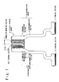
- FIGS. 1 and 2 show a configuration of a flexible printed board according to the first exemplary embodiment.
- FIGS. 3A to 5 are diagrams for showing a folding method of the flexible printed board.
- FIGS. 6 and 7 show a state in which the flexible printed board is mounted to a cellular phone.
- a device for the printed board to be mounted is not limited to cellular phones, needless to say, and may be other electronic devices such as a PDA (Personal Digital Assistant), a personal computer, and an electronic dictionary.
- PDA Personal Digital Assistant
- a flexible printed board 10 is formed approximately symmetrically between the side of a symbol (1) (the right side of FIG. 1 ) and the side of a symbol (2) (the left side of FIG. 1 ), and has two interconnection boards (a first interconnection board section and a second interconnection board section) 2 and 12 with terminal sections formed at both ends. Connection is performed on the side of the one end of the two interconnection boards 2 and 12 (the side of the upper end in FIG. 1 ).
- the interconnection board 2 (the first interconnection board section) provided on the side of the symbol (1) of the flexible printed board 10 has a terminal neighboring section 3 (a first terminal neighboring section) formed on the side of one end thereof (the side of the upper end of FIG. 1 ), a terminal section 5 formed on the side of the other end (the side of the lower end of FIG. 1 ), and an interconnection section 4 (a first interconnection section) in the form of a crank, to which a plurality of interconnections are formed for connecting both the end sections.
- a connector mounting section 1 (a first terminal board section), which is a board provided with terminals, is provided adjacent to the terminal neighboring section 3.
- the connector mounting section 1 is connected with the side of the symbol (2) which is symmetrically formed, as mentioned later.
- the interconnection section 4 is formed by attaching two interconnection layers each other, in which a plurality of interconnections are formed, although being not shown, and corresponding terminals of the connector mounting section 1 and the terminal section 5 provided at both the ends are connected by these interconnections.
- the connector mounting section 1 is formed in an approximately a rectangular shape, and a plurality of male terminals to be mounted on a board of a cellular phone are formed in the connector mounting section 1.
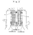
- the plurality of terminals are formed on one side (a terminal formation surface) of the connector mounting section 1. More specifically, as shown in an enlarged view of FIG. 2 , the plurality of terminals 1a are formed in two lines along a longitudinal direction of the connector mounting section 1, namely, parallel to a long side of the rectangular shape.
- the terminal neighboring section 3 of the above-mentioned interconnection board 2 is connected in adjacent to the right side of the connector mounting section 1. More in detail, the terminal neighboring section 3 is formed in parallel along the long side of the rectangular connector mounting section 1 and has approximately the same shape (rectangle) as the connector mounting section 1.
- the interconnections extending from the above-mentioned interconnection section 4 are connected to the respective terminals 1a. At this time, a number of interconnections are accommodated in a space-saved region in the interconnection section 4, since interconnections are formed in two layers.
- the interconnections are arranged on a region wider than the region of the interconnection section 4 in the terminal neighboring section 3 so as to be connected to the terminals 1a arranged along the long side of the connector mounting section 1, as shown symbol 2a of FIG. 2 (part of the interconnections 2a are not shown). That is to say, the interconnections formed in two layers in the width shown in FIG. 1 in the interconnection section 4 are arranged to be distributed over the width of the longitudinal direction (the width of the long side) of the terminal neighboring section 3 to correspond to the positions of the respective terminals 1a in the terminal neighboring section 3, immediately before being connected to the respective terminals 1a of the connector mounting section 1. For this reason, the terminal neighboring section 3 on the interconnection board 2 adjacent to the connector mounting section 1 necessarily has a large area. Additionally, the interconnection section 4 is connected on the side of the short side of the terminal neighboring section 3.
- the connector mounting section 1 and the terminal neighboring section 3 are formed a continuous portion by a single polyimide layer and so forth, and a notch section 3a along the long side and circular through-holes 3b are formed in the boundary of them, to be made weaker in strength than other portions (the periphery).
- the boundary between the connector mounting section 1 and the terminal neighboring section 3 (the two-dot chain line) is formed so as to be foldable, as will be mentioned below.
- the boundary may be formed with low strength using other methods, or the strength of a portion to be folded does not need to be formed with low strength if the strength of the flexible printed board 1 originally has foldable strength.
- the portion (on the left side of FIG. 1 ) indicated by the symbol (2) of the flexible printed board 10 according to the first exemplary embodiment has the same configuration as the portion on the side of the symbol (1) which includes the connector mounting section 1, the interconnection board 2, and the terminal section 5, and the portions are symmetrically formed in a pair with respect to the dotted line in FIG. 1 (a folding line between the terminal board sections) as the center. More in detail, the portions are symmetrically formed so as to be connected to the long side of the connector mounting section 1 on the opposite side to the terminal neighboring section 3, as shown in FIG. 1 . For example, the portions are formed continuously by a single polyimide layer and so forth.
- test terminal section 11 (a second terminal board section) as a board with terminals is provided for a portion connected to the connector mounting section 1.
- the test terminal section 11 is formed as a rectangle in the same way as the connector mounting section 1, and an interconnection board 12 (a second interconnection board section) is connected to the side of the long side opposite to the connection side to the connector mounting section 1.
- the interconnection board 12 and the above-mentioned interconnection board 2 on the right side are symmetrically formed.
- the connector mounting section 1 and the test terminal section 11 are provided to be line-symmetric with the boundary line (the folding line between the terminal board sections).
- respective interconnections 12a are distributed over a wide region in correspondence to terminals 11a, namely, along the long side of the test terminal section 11, in the terminal neighboring section 13 (the second section adjacent to terminals) adjacent to the test terminal section 11, in the other words, over the width wider than the width of an interconnection section 14 (part of the interconnections 12a are not shown), as shown in FIG. 2 .
- These interconnections are accommodated in two layers in the interconnection section 14 (the second interconnection section), extending to a terminal section 15.
- the terminals 1a of the connector mounting section 1 and the terminals 11a of the test terminal section 11 are connected through respective interconnections 2aa (part of the interconnections 2aa are not shown).
- the interconnections 2aa extend to cross the boundary line between the connector mounting section 1 and the test terminal section 11 (the folding line between the terminal board sections).
- a notch section 13a and through-holes 13b are formed on the boundary line between the test terminal section 11 and the terminal neighboring section 13 in the same way as mentioned above, so as to be foldable along the boundary line (see the two-dot chain line).
- the folding line between the connector mounting section 1 and the test terminal section 11 (the folding line between the terminal board sections; see the two-dot chain line) too, has a notch section 1b along the folding line, which is formed to be foldable.
- connection portion the upper portion of the bilaterally symmetric flexible printed board 10
- the connector mounting section 1 and the terminal neighboring section 3 adjacent thereto, and the test terminal section 11 and the terminal neighboring section 13 adjacent thereto are continuously formed by the single polyimide layer and the like, which are approximately equally divided into four as shown by the two-dot chain lines.
- Each of the four sections has a rectangular shape, and the single layer is bendable to make mountain-folds along the respective boundary lines (two-dot chain lines) as mentioned above.
- a metal plate is provided on the surface opposite to a terminal formation surface of the connector mounting section 1 for the purpose of improving the strength of the connector mounting section 1.
- double-sided tapes are provided on both surfaces of each of the terminal neighboring sections 3 and 13, which will be stuck on faces in contact when the respective terminal neighboring sections are folded. It should be noted that other adhesive bonding materials for bonding faces in contact together may be provided instead of the double-sided tape, and bonding material may be applied on (filled into) a bonding face at the time of folding.
- the respective terminal neighboring sections 3 and 13 have been described to have approximately the same shape as the connector mounting section 1 and the test terminal section 11 adjacent thereto.
- the respective terminal neighboring sections 3 and 13 may be a smaller shape than the connector mounting section 1 and the test terminal section 11. That is to say, the respective terminal neighboring sections 3 and 13 may have shape and size so as to hide under the connector mounting section 1 and the test terminal section 11 when being folded on the connector mounting section 1 and the test terminal section 11, as will be mentioned later.
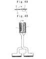
- FIG. 3B shows the flexible printed board 10 at the time of manufacturing before being folded
- FIG. 3A shows only the structure on the side of the upper end (the connector mounting section 1, the test terminal section 11, and the terminal neighboring sections 3 and 13) seen from above. That is to say, FIG. 3A is a side view of the flexible printed board 10 on the side of the terminal board section.
- the terminal neighboring section 3 and 13 positioned at both ends are bended inward at the boundary (folding) lines with the connector mounting section 1 and the test terminal section 11 adjacent thereto (first step).
- the terminal neighboring section 3 and 13 are folded to make mountain-folds on the dotted lines shown in FIG. 3B .
- the terminal neighboring section 3 positioned on the right end is folded to be put on the back side which is opposite to the terminal formation face of the connector mounting section 1.
- the terminal neighboring section 13 positioned on the left side is folded to put on the back side which is opposite to the terminal formation face of the test terminal section 11, as indicated by the arrow in FIG. 3A .
- the terminal neighboring sections 3 and 13 are positioned to be put on the back sides of the connector mounting section 1 and the test terminal section 11 respectively, as shown in FIGS. 4A and 4B .
- the interconnection boards 2 and 12 are positioned with the left and right being reversed.
- surfaces to face each other after folding namely, the backs of the connector mounting section 1 and the terminal neighboring section 3, and the backs of the test terminal section 11 and the terminal neighboring section 13, are each stuck together with the double-sided tapes.
- the flexible printed board 10 is folded to make a mountain-fold along a dotted line shown in FIG. 4B , namely, along a boundary line between the connector mounting section 1 and the test terminal section 11 (the folding line between the terminal board sections) from the state shown in FIGS. 4A and 4B .
- the test terminal section 11 and the terminal neighboring section 13, which are put on each other and positioned on the left side are folded on the side of the connector mounting section 1 and the terminal neighboring section 3, which are put on each other and positioned on the right side, as shown by the arrows in FIGS. 4A and 4B .
- the flexible printed board 10 is folded such that the terminal neighboring sections 3 and 13 oppose to each other and are put on each other.
- the connector mounting section 1 is positioned on the surface side while the test terminal section 11 is positioned on the back side, and the terminal neighboring sections 3 and 13 are layered therebetween, as shown in FIGS. 5A and 5B .
- the terminal neighboring sections 3 and 13, to which the double-sided tape is stuck are fixed to each other.
- the interconnection boards 2 and 12 are also all put on each other.
- the flexible printed board 10 can be formed to have the connector mounting section 1 and the test terminal section 11 on the surface and back sides. Therefore, a mounting region for the connector mounting section 1 is sufficient since the terminal neighboring sections 3 and 13 are put on the connector mounting section 1.
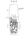
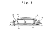
- FIG. 6 shows a folding cellular phone 100 seen from the back side of an operation face, in which an upper section 110 having a display is shown upward and a lower section 120 having an operation face is shown downward.
- FIG. 7 shows a cross sectional state of the lower section 120 along the A-A line.
- the lower section 120 of the cellular phone 100 is surrounded by an operation section 121 and a cover 122 positioned on the back side thereof.
- a main board 123 is layered on the operation section 121.
- the connector mounting section 1 of the flexible printed board 10 folded in the above way is mounted on a part of the main board 123. That is to say, the mounting is possible even in a mounting region for the area of the connector mounting section 1.
- the interconnection boards 2 and 12 put on each other are positioned to go toward the upper section 110 by passing through the hinge section and the terminal sections 5 and 15 are mounted within the upper section 110.
- the flexible printed board having the above-mentioned structure can be mounted even when only a mounting region with the width shown by the symbol W in FIG. 7 can be secured in particular. That is to say, although a mounting region of a portion adjacent to the connector mounting section 1 usually has to be secured, the folding onto the connector mounting section 1 makes it possible to save a space of a mounting region as mentioned above.
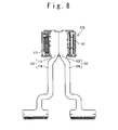
- FIG. 8 Next, another configuration and folding method of the flexible printed board will be described with reference to FIGS. 8 to 11 .
- the configuration shown in FIG. 8 will be described.
- a flexible printed board 110 shown in FIG. 8 has connector mounting sections 101 and 111 (the first terminal board section 101 and the second terminal board section 111) positioned at both ends of the upper end portion, in which terminal neighboring sections 103 and 113 (a first terminal neighboring section 103 and a second terminal neighboring section 113), respectively connected thereto, are positioned therebetween by being connected with each other. That is to say, the board formed by a single polyimide layer and so forth is approximately equally divided into four sections at the upper end portion of the flexible printed board 110, as in FIG. 1 . From the right, the connector mounting section 101, the terminal neighboring section 103 adjacent thereto, the other terminal neighboring section 113, and the other connector mounting section 111 connected thereto, are formed.
- the connector mounting section 101 is provided adjacent to one side of the terminal neighboring section 103.
- the terminal neighboring section 113 is provided adjacent on the other side of the terminal neighboring section 113.
- the connector mounting section 111 is provided adjacent to the terminal neighboring section 113 on the side opposite to the terminal neighboring section 103.
- the terminal neighboring sections 103 and 113 are each formed such that a boundary (folding) line (the chain line in FIG. 8 , the folding line between the terminal board sections) is valley-foldable.
- the connector mounting sections 101 and 111 and the terminal neighboring sections 103 and 113 are each formed such that the boundary (folding) lines thereof (the dotted lines in FIG. 8 ) are mountain-foldable.
- Interconnection boards 102 and 112 (the first interconnection board section 102 and the second interconnection board section 112) of the symmetric shapes are connected from the terminal neighboring sections 103 and 113.
- Interconnection sections 104 and 114 (a first interconnection section 104 and a second interconnection section 114) are connected to the terminal neighboring sections 103 and 113, respectively. That is to say, the terminal neighboring sections 103 and 113 have a bilaterally symmetric shape.
- the connector mounting section 101 and the connector mounting section 111 are axis-symmetrically positioned with respect to the boundary (folding) line between the terminal neighboring sections 101 and 111 (the folding line between the terminal board sections).
- the connector mounting sections 101 and 111 are positioned on the surface and back sides as a result of the folding in accordance with the above-mentioned folding lines, and the terminal neighboring sections 103 and 113 are put therebetween. Consequently, a mounting region can be a minimum space since the connector mounting section 101 and 111, which serve as terminal surfaces, are exposed outside while the terminal neighboring sections 103 and 113 adjacent thereto can be put on each other, as in the first exemplary embodiment.
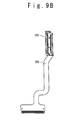
- a flexible printed board 210 of the present invention may be only the structure on the right side indicated by the symbol (1) of the flexible printed board 10 shown in FIG. 1 , as shown by the flexible printed board 210 in FIG. 9A . Consequently, it is possible to save a space of a mounting region in the same way as mentioned above, by folding a terminal neighboring section 203 (first terminal neighboring section), which is adjacent to a connector mounting section 201 (the first terminal board section), to make a mountain-fold along the dotted line in FIG. 9A in order for the terminal neighboring section 203 to be put on the connector mounting section 201.
- a flexible printed board 310 of the present invention may be a configuration in which terminal neighboring sections 303 and 313 (the first terminal neighboring sections 303 and 313) are formed adjacent to the left and right of a connector mounting section 301 (the first terminal board section 301) positioned at the center of the upper end, as shown by the flexible printed board 310 in FIG. 10A . That is to say, the terminal neighboring sections 303 and 313 are connected to both sides of the single connector mounting section 301. In this case, the terminal neighboring section 313 positioned on the left side is firstly folded at the boundary (folding) line (dotted line) with respect to the connector mounting section 301, and is put on the back side of the connector mounting section 301, as shown in FIG. 10A .
- the terminal neighboring section 303 on the right side is folded at the boundary (folding) line (dotted line) with respect to the connector mounting section 301 from the state of FIG. 10B , to be put on the back side of the connector mounting section 301, namely, to be put on the terminal neighboring section 313, which has already been folded.
- the state of FIG. 10C makes it possible to save a space of a mounting region in the same way as mentioned above.
- terminals may be formed on a portion indicated by the symbol 303.
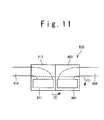
- a flexible printed board of the present invention may be a configuration as shown in FIG. 11 .
- This flexible printed board 410 is formed as a configuration that the structure on the right side indicated by the symbol (1) and the structure on the left side indicated by the symbol (2) of the above-mentioned flexible printed board 10 shown in FIG. 1 , are connected on the side of the upper end. That is to say, two rectangular connector mounting sections 401 and 411 (the first terminal board section 401 and the second terminal board section 411) are arranged in a line to be connected at the short sides while terminal neighboring sections 403 and 413 (the first terminal neighboring section 403 and the terminal neighboring section 413) are formed adjacent to the long sides of the connector mounting sections 401 and 411, respectively.
- a polyimide layer of approximately a rectangular shape is divided into four sections in the form of a cross, in which the connector mounting sections 401 and 411 and the terminal neighboring sections 403 and 413 are formed.
- Interconnection sections 404 and 414 (the first interconnection section 404 and the second interconnection section 414) are connected to the short sides of the terminal neighboring sections 403 and 413.
- a mountain-fold is firstly made along the dotted line such that the two terminal neighboring sections 403 and 413 are put on the back side of the connector mounting sections 401 and 411 adjacent thereto, as indicated by the arrow (1).
- the connector mounting sections 401 and 411 are folded such that a mountain-fold is made along the boundary (folding) line (the chain line; a folding line between the terminal board sections) between the connector mounting sections 401 and 411, as indicated by the arrow (2), in order to be positioned on the surface and back sides.
- the terminal neighboring sections 403 and 413 are positioned to be put on each other between the connector mounting sections 401 and 411, making it possible to save a space of a mounting region.
- the flexible printed board 10 according to the present invention can be mounted on such an electronic apparatus as a cellular phone and has industrial applicability, which in particular, is effective for a folding electronic apparatus in which connection is required between bendable housings.
- the flexible printed board of the present invention is characterized in that the flexible printed board has a terminal section having terminals and an interconnection board section having interconnections to be connected to the terminals, and is formed to be foldable such that a terminal neighboring section adjacent along a longitudinal direction of the terminal board section is put on the side opposite to a terminal formation surface of the terminal board section.
- the terminal neighboring section within the interconnection board section which is adjacent to the terminal board section, is firstly folded to be put on the back side of the terminal board section.
- the terminal board section more terminals are arranged along a longitudinal direction of the terminal board section than a direction different from the longitudinal direction.
- the terminal board section is approximately a rectangular shape, and the terminal neighboring section is formed adjacent to a long side thereof.
- interconnections are arranged over a region wider than other portions of the interconnection board section, in accordance with positions of the respective terminals of the terminal board section.
- the present invention is characterized in that the terminal neighboring section is a shape which is approximately the same as or smaller than the terminal board section. Consequently, it is possible to more effectively save a space since the terminal neighboring section to be put on the terminal board section when being folded does not protrude therefrom.
- the flexible printed board of the present invention is a flexible printed board having a pair of flexible printed boards which include the above-mentioned terminal board sections and interconnection board sections, and is characterized in that the flexible printed board mutually connects both the terminal board sections and/or both the terminal neighboring sections and is symmetrically formed to be foldable with a connection portion.
- the flexible printed board of the present invention is characterized in that a flexible printed board is a pair of flexible printed boards which include terminal board sections and interconnection board sections, and the flexible printed board mutually connects both the terminal board sections while connecting terminals of both the terminal board sections with interconnections, and is symmetrically formed so as to be foldable with respect to this connection portion.
- both terminal board sections are mutually positioned on the surface and back sides and the respective terminal formation surfaces of both the terminal board sections are exposed outside after the folding. Consequently, the flexible printed board having the terminals on both surfaces can be formed in a saved space.
- bonding material for bonding contact faces at the time of folding is provided. Consequently, it is possible to prevent a folded flexible printed board from opening and improve reliability of an apparatus after the mounting.
- the present invention is characterized in that a notch section and/or through-holes are formed at a folding portion, to reduce strength less than other portions. Consequently, the folding is easy and resilience after the folding is lowered to stabilize the folded state, making it possible to improve reliability of an apparatus after the mounting.
- the present invention provides an electronic apparatus to which the above-mentioned flexible printed board is mounted, e.g. a cellular phone.
- a cellular phone e.g. a cellular phone
- a method of folding the above-mentioned flexible printed board according to the present invention is characterized in that a terminal neighboring section is folded toward the side opposite to a terminal formation surface such that the terminal formation surface of a terminal board section is exposed outside.
- the flexible printed board having a pair of flexible printed boards which include terminal board sections and interconnection board sections is folded such that both the terminal board sections are positioned on the surface and back sides and each terminal formation surface is exposed outside, as mentioned above.
- the present invention is characterized that each terminal neighboring section is folded on the back sides of the terminal board sections adjacent thereto, and further folded such that the folded terminal neighboring sections oppose to each other, in order to position both the terminal board sections on the surface and back sides and expose the terminal formation surfaces outside.
Landscapes
- Engineering & Computer Science (AREA)
- Microelectronics & Electronic Packaging (AREA)
- Structure Of Printed Boards (AREA)
- Combinations Of Printed Boards (AREA)
- Printing Elements For Providing Electric Connections Between Printed Circuits (AREA)
- Telephone Set Structure (AREA)
Applications Claiming Priority (2)
| Application Number | Priority Date | Filing Date | Title |
|---|---|---|---|
| JP2006201448A JP2008028276A (ja) | 2006-07-25 | 2006-07-25 | フレキシブルプリント基板及びこれを実装した電子機器並びにフレキシブルプリント基板の折り畳み方法 |
| PCT/JP2007/063976 WO2008013070A1 (en) | 2006-07-25 | 2007-07-13 | Flexible printed board, electronic device mounted with this, and flexible printed board folding method |
Publications (3)
| Publication Number | Publication Date |
|---|---|
| EP2046103A1 true EP2046103A1 (de) | 2009-04-08 |
| EP2046103A4 EP2046103A4 (de) | 2010-02-24 |
| EP2046103B1 EP2046103B1 (de) | 2011-09-14 |
Family
ID=38981383
Family Applications (1)
| Application Number | Title | Priority Date | Filing Date |
|---|---|---|---|
| EP07790757A Not-in-force EP2046103B1 (de) | 2006-07-25 | 2007-07-13 | Flexible leiterplatte, damit versehene elektronische anordnung und faltverfahren für eine flexible leiterplatte |
Country Status (5)
| Country | Link |
|---|---|
| US (1) | US8115103B2 (de) |
| EP (1) | EP2046103B1 (de) |
| JP (1) | JP2008028276A (de) |
| CN (1) | CN101496455B (de) |
| WO (1) | WO2008013070A1 (de) |
Cited By (2)
| Publication number | Priority date | Publication date | Assignee | Title |
|---|---|---|---|---|
| WO2010070017A1 (en) * | 2008-12-19 | 2010-06-24 | Nokia Corporation | Apparatus and methods |
| EP4700945A3 (de) * | 2020-06-02 | 2026-03-18 | Samsung Electronics Co., Ltd. | Elektronische vorrichtung mit mehreren leiterplatten |
Families Citing this family (16)
| Publication number | Priority date | Publication date | Assignee | Title |
|---|---|---|---|---|
| TW201039520A (en) * | 2009-04-28 | 2010-11-01 | Adv Flexible Circuits Co Ltd | Flat signal transmission cable with bundling structure |
| JP2010287658A (ja) * | 2009-06-10 | 2010-12-24 | Lenovo Singapore Pte Ltd | フレキシブルプリント基板 |
| WO2010150825A1 (ja) * | 2009-06-25 | 2010-12-29 | オリンパスメディカルシステムズ株式会社 | 撮像ユニット |
| JP5446790B2 (ja) * | 2009-12-02 | 2014-03-19 | セイコーエプソン株式会社 | 電気光学装置および電子機器 |
| KR101786512B1 (ko) * | 2010-07-26 | 2017-10-18 | 엘지전자 주식회사 | 다층 연성회로기판의 제조방법 |
| CN102480840B (zh) * | 2010-11-24 | 2014-06-25 | 富葵精密组件(深圳)有限公司 | 电路板的制作方法 |
| US9084368B2 (en) * | 2011-06-15 | 2015-07-14 | Novatek Microelectronics Corp. | Single FPC board for connecting multiple modules and touch sensitive display module using the same |
| US9131605B2 (en) * | 2012-05-25 | 2015-09-08 | Nitto Denko Corporation | Dynamic loop with fold |
| CN103582317B (zh) * | 2013-10-16 | 2016-07-06 | 镇江华印电路板有限公司 | 挠性印制线路板漏锡半圆孔制作方法 |
| CN104837294B (zh) * | 2015-04-09 | 2017-07-11 | 京东方科技集团股份有限公司 | 一种柔性电路板及其制备方法和显示装置 |
| JP6862754B2 (ja) * | 2016-10-17 | 2021-04-21 | 大日本印刷株式会社 | 回路基板、回路装置および情報記録装置 |
| CN109983851A (zh) * | 2017-10-25 | 2019-07-05 | 深圳市大疆创新科技有限公司 | 柔性电路板及电子装置 |
| US12101882B2 (en) | 2019-03-04 | 2024-09-24 | Gigalane Co., Ltd. | Flexible circuit board and wireless terminal comprising same |
| KR102758032B1 (ko) * | 2019-08-02 | 2025-01-21 | 삼성전자주식회사 | Fpcb를 포함하는 전자 장치 |
| JP6824361B1 (ja) * | 2019-10-25 | 2021-02-03 | 三菱電機株式会社 | インバータ装置 |
| DE102024128498A1 (de) * | 2024-10-02 | 2026-04-02 | Drägerwerk AG & Co. KGaA | Leiterplatte für den Einbau in ein Elektrogerät |
Family Cites Families (17)
| Publication number | Priority date | Publication date | Assignee | Title |
|---|---|---|---|---|
| JPH04263495A (ja) * | 1991-02-18 | 1992-09-18 | Ibiden Co Ltd | フレキシブル配線板 |
| JP2744889B2 (ja) * | 1994-09-29 | 1998-04-28 | インターナショナル・ビジネス・マシーンズ・コーポレイション | 磁気ディスク装置のフレキシブルケーブル構造 |
| JP3435245B2 (ja) * | 1995-02-21 | 2003-08-11 | ペンタックス株式会社 | フレキシブルプリント配線板 |
| US6118666A (en) * | 1998-01-12 | 2000-09-12 | Asahi Kogaku Kogyo Kabushiki Kaisha | Flexible printed wiring board and connecting structure thereof |
| US6153832A (en) * | 1999-02-08 | 2000-11-28 | Hewlett-Packard Company | Z-fold printhead carriage trailing cable for optimized panelization |
| JP3773782B2 (ja) * | 2000-10-31 | 2006-05-10 | 三洋電機株式会社 | 折畳式携帯電話端末 |
| JP2003158355A (ja) * | 2001-11-20 | 2003-05-30 | Kenwood Corp | フレキシブルプリント基板の接続構造および電子機器 |
| JP4319385B2 (ja) * | 2002-10-10 | 2009-08-26 | 株式会社東芝 | 移動通信端末装置及びフレキシブル基板 |
| JP4136695B2 (ja) * | 2003-02-10 | 2008-08-20 | 住友電工プリントサーキット株式会社 | フレキシブルプリント基板 |
| JP4121391B2 (ja) | 2003-02-17 | 2008-07-23 | 三洋電機株式会社 | フレキシブルプリント基板及びフレキシブルプリント基板を有する折り畳み式電子機器 |
| JP3098782U (ja) | 2003-06-24 | 2004-03-11 | 住友電工プリントサーキット株式会社 | フレキシブルプリント基板 |
| JP4087311B2 (ja) | 2003-08-06 | 2008-05-21 | シャープ株式会社 | 携帯機器 |
| JP4543772B2 (ja) | 2003-09-19 | 2010-09-15 | セイコーエプソン株式会社 | 電気光学装置および電子機器 |
| JP4206017B2 (ja) * | 2003-09-22 | 2009-01-07 | 住友電工プリントサーキット株式会社 | フレキシブルプリント基板 |
| JP4159529B2 (ja) * | 2004-10-07 | 2008-10-01 | 埼玉日本電気株式会社 | 折り畳み型機器のヒンジ部構造 |
| TW200710672A (en) * | 2005-09-02 | 2007-03-16 | Adv Flexible Circuits Co Ltd | Circuit connection bus cable capable of changing corresponding pins |
| JP2007109343A (ja) * | 2005-10-14 | 2007-04-26 | Hitachi Global Storage Technologies Netherlands Bv | フレキシブル・ケーブルの位置決め構造および磁気ディスク装置 |
-
2006
- 2006-07-25 JP JP2006201448A patent/JP2008028276A/ja active Pending
-
2007
- 2007-07-13 CN CN2007800286736A patent/CN101496455B/zh not_active Expired - Fee Related
- 2007-07-13 US US12/374,368 patent/US8115103B2/en not_active Expired - Fee Related
- 2007-07-13 WO PCT/JP2007/063976 patent/WO2008013070A1/ja not_active Ceased
- 2007-07-13 EP EP07790757A patent/EP2046103B1/de not_active Not-in-force
Cited By (3)
| Publication number | Priority date | Publication date | Assignee | Title |
|---|---|---|---|---|
| WO2010070017A1 (en) * | 2008-12-19 | 2010-06-24 | Nokia Corporation | Apparatus and methods |
| US8043115B2 (en) | 2008-12-19 | 2011-10-25 | Nokia Corporation | Apparatus and methods |
| EP4700945A3 (de) * | 2020-06-02 | 2026-03-18 | Samsung Electronics Co., Ltd. | Elektronische vorrichtung mit mehreren leiterplatten |
Also Published As
| Publication number | Publication date |
|---|---|
| WO2008013070A1 (en) | 2008-01-31 |
| EP2046103B1 (de) | 2011-09-14 |
| EP2046103A4 (de) | 2010-02-24 |
| US20100016039A1 (en) | 2010-01-21 |
| US8115103B2 (en) | 2012-02-14 |
| CN101496455B (zh) | 2013-05-22 |
| CN101496455A (zh) | 2009-07-29 |
| JP2008028276A (ja) | 2008-02-07 |
Similar Documents
| Publication | Publication Date | Title |
|---|---|---|
| EP2046103B1 (de) | Flexible leiterplatte, damit versehene elektronische anordnung und faltverfahren für eine flexible leiterplatte | |
| JP4552565B2 (ja) | フレキシブル配線基板及び折り畳み式電子機器 | |
| CN109121285B (zh) | 一种电路板结构及电子设备 | |
| WO2009154335A1 (en) | Printed circuit board electrically connected to the ground of electronic device | |
| KR20090044704A (ko) | 연성인쇄회로기판, 이의 접합방법 및 이를 구비하는 배터리팩 | |
| JP4014575B2 (ja) | フレキシブル基板用コネクタ付き回路基板および回路基板とフレキシブル基板との接続構造 | |
| KR101406045B1 (ko) | 시일 구조체 | |
| JP3992470B2 (ja) | ケーブル部を有するフレキシブルプリント基板 | |
| JP2010040929A (ja) | 電子機器及びフレキシブルプリント配線板 | |
| JPH11258621A (ja) | 可撓性配線基板、液晶表示装置、電子機器 | |
| KR20110045721A (ko) | 휴대 단말기용 인쇄회로기판 | |
| JP4121391B2 (ja) | フレキシブルプリント基板及びフレキシブルプリント基板を有する折り畳み式電子機器 | |
| US8835761B2 (en) | Sealing structure | |
| JP2002289764A (ja) | フレキシブル回路基板、それを用いた表示装置および電子機器 | |
| JP6323622B2 (ja) | 部品実装基板 | |
| JP4793230B2 (ja) | フレキシブルプリント基板 | |
| JP5029953B2 (ja) | シール構造体 | |
| JP4309230B2 (ja) | 携帯端末装置及びフレキシブルプリント配線板 | |
| JP2002158419A (ja) | フレキシブル配線基板及びそれを用いた電気・電子機器 | |
| JP2003309354A (ja) | プリント配線基板の接続方法及びプリント配線基板 | |
| KR20050061960A (ko) | 정전기 제거 특성이 강화된 에프피씨비가 구비된 이동통신 단말기 | |
| JP4318554B2 (ja) | フレキシブル配線回路基板 | |
| JP4899804B2 (ja) | フレキシブルプリント配線基板 | |
| KR20080044927A (ko) | 인쇄회로기판과의 결합력을 향상시킬 수 있는 구조의 표면실장형 카메라 모듈 | |
| JP4856234B2 (ja) | 電子機器 |
Legal Events
| Date | Code | Title | Description |
|---|---|---|---|
| PUAI | Public reference made under article 153(3) epc to a published international application that has entered the european phase |
Free format text: ORIGINAL CODE: 0009012 |
|
| 17P | Request for examination filed |
Effective date: 20090122 |
|
| AK | Designated contracting states |
Kind code of ref document: A1 Designated state(s): AT BE BG CH CY CZ DE DK EE ES FI FR GB GR HU IE IS IT LI LT LU LV MC MT NL PL PT RO SE SI SK TR |
|
| AX | Request for extension of the european patent |
Extension state: AL BA HR MK RS |
|
| DAX | Request for extension of the european patent (deleted) | ||
| RBV | Designated contracting states (corrected) |
Designated state(s): DE FR GB IT |
|
| A4 | Supplementary search report drawn up and despatched |
Effective date: 20100127 |
|
| RIC1 | Information provided on ipc code assigned before grant |
Ipc: H05K 1/02 20060101AFI20101116BHEP Ipc: H05K 1/11 20060101ALI20101116BHEP Ipc: H05K 3/40 20060101ALI20101116BHEP |
|
| GRAP | Despatch of communication of intention to grant a patent |
Free format text: ORIGINAL CODE: EPIDOSNIGR1 |
|
| RTI1 | Title (correction) |
Free format text: FLEXIBLE PRINTED BOARD, ELECTRONIC DEVICE EQUIPPED WITH IT, AND FLEXIBLE PRINTED BOARD FOLDING METHOD |
|
| RIN1 | Information on inventor provided before grant (corrected) |
Inventor name: TOKUYAMA, MAYUMI |
|
| GRAS | Grant fee paid |
Free format text: ORIGINAL CODE: EPIDOSNIGR3 |
|
| GRAA | (expected) grant |
Free format text: ORIGINAL CODE: 0009210 |
|
| AK | Designated contracting states |
Kind code of ref document: B1 Designated state(s): DE FR GB IT |
|
| REG | Reference to a national code |
Ref country code: GB Ref legal event code: FG4D |
|
| REG | Reference to a national code |
Ref country code: DE Ref legal event code: R096 Ref document number: 602007017227 Country of ref document: DE Effective date: 20111208 |
|
| PLBE | No opposition filed within time limit |
Free format text: ORIGINAL CODE: 0009261 |
|
| STAA | Information on the status of an ep patent application or granted ep patent |
Free format text: STATUS: NO OPPOSITION FILED WITHIN TIME LIMIT |
|
| 26N | No opposition filed |
Effective date: 20120615 |
|
| REG | Reference to a national code |
Ref country code: DE Ref legal event code: R097 Ref document number: 602007017227 Country of ref document: DE Effective date: 20120615 |
|
| PGFP | Annual fee paid to national office [announced via postgrant information from national office to epo] |
Ref country code: IT Payment date: 20120725 Year of fee payment: 6 |
|
| PG25 | Lapsed in a contracting state [announced via postgrant information from national office to epo] |
Ref country code: IT Free format text: LAPSE BECAUSE OF NON-PAYMENT OF DUE FEES Effective date: 20130713 |
|
| REG | Reference to a national code |
Ref country code: GB Ref legal event code: 732E Free format text: REGISTERED BETWEEN 20141023 AND 20141029 |
|
| REG | Reference to a national code |
Ref country code: FR Ref legal event code: TP Owner name: LENOVO INNOVATIONS LIMITED (HONG KONG), HK Effective date: 20141119 |
|
| REG | Reference to a national code |
Ref country code: FR Ref legal event code: PLFP Year of fee payment: 10 |
|
| PGFP | Annual fee paid to national office [announced via postgrant information from national office to epo] |
Ref country code: FR Payment date: 20160613 Year of fee payment: 10 |
|
| PGFP | Annual fee paid to national office [announced via postgrant information from national office to epo] |
Ref country code: GB Payment date: 20160713 Year of fee payment: 10 Ref country code: DE Payment date: 20160705 Year of fee payment: 10 |
|
| REG | Reference to a national code |
Ref country code: DE Ref legal event code: R119 Ref document number: 602007017227 Country of ref document: DE |
|
| GBPC | Gb: european patent ceased through non-payment of renewal fee |
Effective date: 20170713 |
|
| REG | Reference to a national code |
Ref country code: FR Ref legal event code: ST Effective date: 20180330 |
|
| PG25 | Lapsed in a contracting state [announced via postgrant information from national office to epo] |
Ref country code: GB Free format text: LAPSE BECAUSE OF NON-PAYMENT OF DUE FEES Effective date: 20170713 Ref country code: DE Free format text: LAPSE BECAUSE OF NON-PAYMENT OF DUE FEES Effective date: 20180201 |
|
| PG25 | Lapsed in a contracting state [announced via postgrant information from national office to epo] |
Ref country code: FR Free format text: LAPSE BECAUSE OF NON-PAYMENT OF DUE FEES Effective date: 20170731 |