EP2048706A1 - Übertragungsverfahren mit einer Behandlung einer zu verbindenden Oberfläche - Google Patents
Übertragungsverfahren mit einer Behandlung einer zu verbindenden Oberfläche Download PDFInfo
- Publication number
- EP2048706A1 EP2048706A1 EP08166193A EP08166193A EP2048706A1 EP 2048706 A1 EP2048706 A1 EP 2048706A1 EP 08166193 A EP08166193 A EP 08166193A EP 08166193 A EP08166193 A EP 08166193A EP 2048706 A1 EP2048706 A1 EP 2048706A1
- Authority
- EP
- European Patent Office
- Prior art keywords
- wafer
- carried out
- bonded
- treatment
- implantation
- Prior art date
- Legal status (The legal status is an assumption and is not a legal conclusion. Google has not performed a legal analysis and makes no representation as to the accuracy of the status listed.)
- Granted
Links
Images


Classifications
-
- H—ELECTRICITY
- H10—SEMICONDUCTOR DEVICES; ELECTRIC SOLID-STATE DEVICES NOT OTHERWISE PROVIDED FOR
- H10P—GENERIC PROCESSES OR APPARATUS FOR THE MANUFACTURE OR TREATMENT OF DEVICES COVERED BY CLASS H10
- H10P14/00—Formation of materials, e.g. in the shape of layers or pillars
- H10P14/20—Formation of materials, e.g. in the shape of layers or pillars of semiconductor materials
-
- H—ELECTRICITY
- H10—SEMICONDUCTOR DEVICES; ELECTRIC SOLID-STATE DEVICES NOT OTHERWISE PROVIDED FOR
- H10P—GENERIC PROCESSES OR APPARATUS FOR THE MANUFACTURE OR TREATMENT OF DEVICES COVERED BY CLASS H10
- H10P90/00—Preparation of wafers not covered by a single main group of this subclass, e.g. wafer reinforcement
- H10P90/19—Preparing inhomogeneous wafers
- H10P90/1904—Preparing vertically inhomogeneous wafers
- H10P90/1906—Preparing SOI wafers
- H10P90/1914—Preparing SOI wafers using bonding
- H10P90/1916—Preparing SOI wafers using bonding with separation or delamination along an ion implanted layer, e.g. Smart-cut
-
- H—ELECTRICITY
- H10—SEMICONDUCTOR DEVICES; ELECTRIC SOLID-STATE DEVICES NOT OTHERWISE PROVIDED FOR
- H10W—GENERIC PACKAGES, INTERCONNECTIONS, CONNECTORS OR OTHER CONSTRUCTIONAL DETAILS OF DEVICES COVERED BY CLASS H10
- H10W10/00—Isolation regions in semiconductor bodies between components of integrated devices
- H10W10/10—Isolation regions comprising dielectric materials
- H10W10/181—Semiconductor-on-insulator [SOI] isolation regions, e.g. buried oxide regions of SOI wafers
Definitions
- the invention generally concerns the manufacturing of multilayer wafer including materials selected from semiconductor materials, and used in applications in microelectronics, optics, optoelectronics and/or optronics.
- the invention concerns the processes for transferring from a "top” wafer (or donor wafer - these terms being herein understood as equivalent) a layer of a semiconductor material onto a "handle” (or receiving wafer, or “base” wafer - these terms being herein understood as equivalent), in order to make a multilayer wafer.
- the known types of BTP processes include:
- the bonding step of such processes is generally performed without adding between the top and handle wafers any adhesive (such as a resin).
- the surfaces to be bonded must be very smooth (i-e. present a very low roughness).
- a bonding of the surfaces of two wafers generates between the bonded surfaces a bonding interface associated with a given bonding energy (the higher this energy the stronger the bond).
- the bonding energy obtained by direct bonding two wafers without any additional treatment is sometimes not high enough.
- such BHT is generally carried out at high temperatures (i.e. at temperatures of 900°C or higher).
- high temperatures i.e. at temperatures of 900°C or higher.
- HT BHT high temperature BHT carried out at temperature higher than 900°C.
- Such HT BHT reinforces the bonding interface and can bring its bonding energy up to a desired level.
- the bonding energy between a Si wafer and a Si or SiO2 wafer is maximized after a HT BHT at temperatures in the order of 1100-1200°C.
- the bonding energy obtained after a HT BHT can e.g. be 2 to 2.5 J/m 2 for a bonding of Si/Si, SiO 2 /SiO 2 , or Si/SiO 2 .
- Such HT BHT can therefore allow the manufacturing of multilayer wafers with adequate bonding energy between the bonded layers of the wafer.
- the layers associated to different CTEs will undergo expansions of different magnitudes when exposed to a HT BHT. This can lead to negative effects such as a warp of the wafers, or even the generation of defects such as dislocations in the crystalline structure of the wafers.
- a HT BHT on a bonded multilayer wafer for other reasons, e.g. the wafer already comprises components totally or partially elaborated (such wafer is usually called "structured substrate"), or the material of the wafer is likely to be altered by a high temperature treatment (e.g. case of a wafer comprising sharp doping profile like boron, phosphorous or comprising metastable layers that would be altered by HT BUT, like low k materials, high k materials or comprising layers with metallic elements like Al 2 O 3 or TiN),
- a high temperature treatment e.g. case of a wafer comprising sharp doping profile like boron, phosphorous or comprising metastable layers that would be altered by HT BUT, like low k materials, high k materials or comprising layers with metallic elements like Al 2 O 3 or TiN
- the surfaces to be bonded are "activated" by their exposure to a plasma, before being contacted together.
- Plasma activation is advantageous since it allows obtaining high bonding energy with a BHT which is carried out after contacting the surfaces to be bonded, but which remains limited to a low temperature BHT ("LT BHT").
- This article discloses a Smart Cut TM -type process in which prior to the wafer bonding step (between a top and a handle wafers) a plasma activation can be carried out on the surfaces to be bonded.
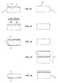
- figure 1 The general principle of such process is illustrated in figure 1 , which comprises figures 1a to 1e to show the successive main steps of such a known principle.
- Figure 1a shows a top wafer 10, and a handle wafer 20.
- the top wafer 10 has been implanted with one or more species in order to form an embrittlement zone 11.
- This top wafer 10 is covered by an insulator layer 12.
- the surface 100 of this insulator layer is to be contacted with a surface 200 of the handle wafer, for a direct bonding.
- Figure 1b shows the activation of the front surfaces 100 and 200 by a plasma, in a plasma chamber.
- this activation creates an activated region 101 on the front surface 100 of the top wafer 10, and an activated region 201 on the front surface 200 of the handle wafer 20.
- This activation also generates contaminants due to the exposure of the wafers to a plasma.
- Such contaminants are more particularly illustrated by references 111 and 211 on the respective back faces 110, 210 of the wafers, as the front faces receive significantly less contaminants than the back faces (as an example, the plasma activation of a silicon wafer typically generates a contaminant concentration of about 2.10 10 atoms/cm 2 on the "front" surface which is to be activated and which faces the inner space of the plasma chamber, the contaminant concentration being above 10 11 atoms/cm 2 on the back surface of the wafer).
- the wafer is disposed on a chuck in the plasma chamber.
- the chuck is adapted to perform the following functions:
- This set of functions that have to be performed by the chuck leads to selecting for making the chuck materials containing elements that are likely to contaminate the surface of the wafer in contact with said chuck (i.e. the back surface of the wafer, since it is the front surface which is directly exposed to the plasma).
- This material can typically be Al 2 O 3 based sintered ceramics.
- Figure 1d illustrates the direct bonding of top wafer 10 and handle wafer 20, these two wafers being bonded by their front surfaces. This bonding generates a multilayer 30 wafer (referred to as an "intermediate" multilayer wafer) which comprises in particular the embrittlement zone 11.
- Figure 1e hen illustrates the multilayer wafer 35 obtained after a detachment carried out at the embrittlement zone.
- This wafer 35 can be of the type SOI (Silicon On Insulator), SGOI (SiliconGermanium On Insulator), sSOI (strained Silicon On Insulator), GeOI (Germanium On Insulator), SiCOI (Silicon Carbide On insulator), SOQ (Silicon On Quartz), or any other type.
- SOI Silicon On Insulator
- SGOI Silicon Germanium On Insulator
- sSOI strained Silicon On Insulator
- GeOI Germanium On Insulator
- SiCOI Silicon Carbide On insulator
- SOQ Silicon On Quartz
- Figure 1e also illustrates the remaining part of the top wafer (part 15), which has been detached. This part can be treated and reused for a new process, e.g. for constituting a new top or a new handle wafer.
- This type of process illustrates that plasma activation could be advantageous for making multilayer wafers through a DBTP.
- plasma activation is in itself associated with another drawback, related to the contaminants generated by the activation.
- plasma activation generates a contamination of the wafer which is exposed to the plasma, in particular on the back surface of the wafer.
- This "contamination” corresponds to a deposit of metallic elements (e.g. Al, Fe, Ni, Zn, Cr, Ti, Ca, Mg, Y, altogether that may be incorporated in fine particles, on the surface of the wafer, or absorbed in said surface in the case of isolated atoms, molecules or ions.
- metallic elements e.g. Al, Fe, Ni, Zn, Cr, Ti, Ca, Mg, Y, .
- Such deposit of metallic elements can be observed with levels of contamination in the order of 5.10 11 - 5.10 12 atoms/cm 2 on at least some areas of the surface of the exposed wafer.
- Such concentrations are too high for a multilayer wafer which is to be subject to further thermal treatments (e.g. a high temperature annealing at temperatures above 1000°C for smoothing the surface of the wafer, or further treatments carried out on the multilayer wafer for integrating components into the wafer).
- further thermal treatments e.g. a high temperature annealing at temperatures above 1000°C for smoothing the surface of the wafer, or further treatments carried out on the multilayer wafer for integrating components into the wafer).
- the invention proposes a method for transferring from a top donor wafer a layer of material onto a receiving handle wafer, the top and receiving wafers comprising respective surfaces to be bonded, the method comprising:
- Figure 2 (which comprises figures 2a-2e ) shows the main steps of a first embodiment of the invention.
- Figure 2a thus shows a top wafer 10 with an implanted embrittlement zone 11, and a handle wafer 20.
- the front surfaces 100 and 200 of top wafer 10 and handle wafer 20 can undergo preliminary treatments for preparing the surfaces to be bonded.
- These preliminary treatments can include a Chemical-Mechanical Polishing (CMP) and/or one or more cleanings with a cleaning solution (such as RCA, SPM+RCA, ).
- CMP Chemical-Mechanical Polishing
- a cleaning solution such as RCA, SPM+RCA, .
- the top wafer 10 can be made of Si, SiGe, Ge, SiC, or in any other semiconductor material.
- the handle wafer 20 can be made of Si, fused silica, SiC, glass (all these materials being possibly in crystalline, polycrystalline or amorphous form), or in any other semiconductor material.
- the embrittlement zone 11 can have been made by introduction of species in the top wafer (this "introduction being carried out e.g. as an implantation and/or by diffusion, or by any other known technique).
- the "introduction" of species is an implantation of species
- such implantation can be an implantation of only one species (such as e.g. H or He). It can also have been made by implantation of several species (i.e. co-implantation), for example H and He.
- the front surface 100 of the top wafer is the surface of an oxide layer (e.g. a deposit of SiO2, or an oxidized region of the underlying material).
- an oxide layer e.g. a deposit of SiO2, or an oxidized region of the underlying material.
- Figure 2b illustrates an activation step, during which the front surface 100 of the top is exposed to a plasma.
- This activation step like all activation steps mentioned in the different embodiments described in this text - more generally corresponds to a treatment step of a surface to be bonded, with a generation of a contamination on the surface of the wafer which is opposite to the surface treated.
- the back surface 110 of top 10 is therefore covered by a region 111 which is contaminated with metallic contaminants such as those mentioned above (see figure 2c ).
- this contamination on the back surface of the top wafer corresponds to contaminant concentrations which is typically higher than the maximum concentration generally tolerated.
- the handle wafer 20 is not exposed to any plasma. Therefore, no contamination is deposited on the surfaces of said handle wafer.
- the following step is the direct bonding of the top wafer and the handle wafer, for making an intermediate multilayer wafer 30 ( Figure 2d ).
- this removal is carried out by detaching the excess material as delimited in the top by the embrittlement zone 11.
- the remainder 15 of the top is detached from the intermediate wafer 30.
- the removal can also be carried out according to any method known for BTPs.
- This removal can therefore be carried out by etching the back face of the top wafer 10 (i.e. the face of the top wafer which is opposed to the front surface 100), on the intermediate wafer 30.
- the removal step can also be performed in accordance with the ELTRAN ® method.
- embrittlement zone has previously been made by porous material, and here again no implantation is necessary.
- the multilayer wafer 35 obtained does not comprise a heavy contamination generated on a back surface of a wafer whose front surfaces would have been exposed to a plasma for its activation.
- this multilayer wafer shall then undergo additional thermal treatments, some of these thermal treatments being as mentioned before carried out at high temperatures (e.g. smoothing annealing at temperatures above 1000°C).
- this first embodiment of the invention allows to make a multilayer wafer with a DBTP, without having said multilayer wafer polluted by a heavy concentration of contaminants.
- the contaminant concentrations which can be observed on the front face of the exposed top after the activation step are in the order of 2.10 10 atoms/cm2, which is a generally acceptable concentration level.
- the removal step illustrated in figure 2e is carried out by detaching the top wafer at the implanted embrittlement zone 11.
- This detachment can result from a mechanical and/or thermal action.
- the temperature should be kept at moderated values, in order to avoid any diffusion of contaminants which would have been generated on the front surfaces 100, 200 (and would therefore be located in the vicinity of the bonding interface).
- Typical values of moderated temperatures for such splitting annealing are 300-500°C, for a multilayer wafer such as an SOI.
- the implantation of the top for creating the embrittlement zone 11 can advantageously be made with more than one species (co-implantation, e.g. of H+He).
- co-implantation allows a reduction of the temperature for the splitting annealing ; the splitting at an embrittlement zone created by co-implantation (e.g; H+He into a Si top wafer) occurs (for a given global implantation dose - i.e. the sum of the doses of all implanted species-which can typically be a "standard" implantation dose of e.g. 5.10 16 atoms/cm 2 - and more generally a few 10 16 atoms/cm 2 ) at lower temperatures than it would have occurred in the same top wafer implanted with the same global implantation dose, but with only one species.
- a standard implantation dose of e.g. 5.10 16 atoms/cm 2 - and more generally a few 10 16 atoms/cm 2
- a co-implantation (e.g. with H+He) therefore constitutes a favourable feature for performing a splitting annealing at moderated temperatures as mentioned above. And such co-implantation even allows a further reduction of the temperature for the splitting annealing.
- this temperature can remain under 350°C - it can in particular be in a range as low as 200-300°C.
- Figure 3 (which comprises figures 3a-3f ) shows the main steps of a second embodiment of the invention.
- Figure 3a illustrates - as figures 1a and 2a - a top wafer 10 and a handle wafer 20.
- the materials of the top and the handle wafers can be the identical to the materials mentioned in reference to the first embodiment described above.
- the top wafer has been implanted with one or more species for generating an embrittlement zone 11.
- implanted embrittlement zone is only a particular illustration corresponding to the case where the invention is embodied with a Smart Cut TM -type method, whereas any type of DBTP can be used.
- Figure 3b illustrates the step of activation through exposure to a plasma.
- the front surface of the top wafer 10 and/or of the handle wafer 20 can be exposed.
- the first embodiment described above can be combined with the second embodiment.
- Figures 3b-3d illustrate the particular case where both top and handle wafers are activated by a plasma.
- Figure 3c thus illustrates highly contaminated regions 111 and 211 respectively associated to the back surfaces of the top and the handle wafers.
- Figure 3d illustrates the direct bonding of the top and handle wafers, with their front surfaces contacted.
- the bonding is followed (preferably immediately followed) by a cleaning step ( figure 3e ) for removing the contaminants from the highly contaminated regions 111 and 211 on the intermediate multilayer wafer 30 (or from the region 111 or 211 which has been formed, if only one such highly contaminated region has been formed because only one wafer was activated by a plasma before bonding).
- the region 111 is said to be associated to a first "main" surface of the intermediate multilayer wafer 30, and the region 211 is said to be associated to a second "main” surface of the intermediate multilayer wafer 30.
- This cleaning step is carried out on the intermediate multilayer wafer 30 which has been made by the direct bonding of the top and handle wafers, with a cleaning solution able to eliminate contaminants.
- a SC2 solution or a HF solution can be used for that purpose.
- the cleaning step is carried out before the wafer undergoes any high temperature treatment (i.e. any thermal treatment above 900°C).
- the "cleaning step" illustrated in figure 3e can be composed of several successive cleanings.
- Such cleaning is carried out on the intermediate multilayer wafer 30. This differs from the cleaning operations known in the art since these cleaning are usually carried out on single-layer wafers such as bulk silicon wafers.
- Each cleaning of the cleaning step can be carried out as a wet cleaning, i.e. by immersing the wafer to be cleaned in a bath made of the cleaning solution.
- this second embodiment which has the cleaning performed after the bonding, further allows to use a solution such as a SC2 or HF solution, which is known to efficiently remove metallic contaminants.
- a SC2 or HF solution would indeed have been associated to problems if used for cleaning the top and/or handle wafer before their bonding together : in such case, the SC2 or HF solution would have removed the undesirable contaminants, but would also have deactivated the surfaces to be bonded - thus losing the benefit of the plasma activation.
- Figure 3f illustrates the removal step of the excess material of the top.
- An advantage of this second embodiment is that in the case of a removal carried out in a way which generates a remainder (as illustrated in the left part of figure 3f ), such remainder has already been cleaned by the cleaning step.
- the invention ensures that no wafer surfaces can undergo high temperature thermal treatments if said surface is heavily contaminated.
Landscapes
- Pressure Welding/Diffusion-Bonding (AREA)
- Threshing Machine Elements (AREA)
- Container, Conveyance, Adherence, Positioning, Of Wafer (AREA)
- Mechanical Treatment Of Semiconductor (AREA)
Applications Claiming Priority (2)
| Application Number | Priority Date | Filing Date | Title |
|---|---|---|---|
| EP04769581A EP1792337B1 (de) | 2004-09-21 | 2004-09-21 | Übertragungsverfahren mit einer behandlung einer zu verbindenden oberfläche |
| PCT/IB2004/003275 WO2006032946A1 (en) | 2004-09-21 | 2004-09-21 | Transfer method with a treatment of a surface to be bonded |
Related Parent Applications (2)
| Application Number | Title | Priority Date | Filing Date |
|---|---|---|---|
| EP04769581A Division EP1792337B1 (de) | 2004-09-21 | 2004-09-21 | Übertragungsverfahren mit einer behandlung einer zu verbindenden oberfläche |
| EP04769581.2 Division | 2004-09-21 |
Publications (2)
| Publication Number | Publication Date |
|---|---|
| EP2048706A1 true EP2048706A1 (de) | 2009-04-15 |
| EP2048706B1 EP2048706B1 (de) | 2012-12-12 |
Family
ID=34959038
Family Applications (2)
| Application Number | Title | Priority Date | Filing Date |
|---|---|---|---|
| EP04769581A Expired - Lifetime EP1792337B1 (de) | 2004-09-21 | 2004-09-21 | Übertragungsverfahren mit einer behandlung einer zu verbindenden oberfläche |
| EP08166193A Expired - Lifetime EP2048706B1 (de) | 2004-09-21 | 2004-09-21 | Übertragungsverfahren mit einer Behandlung einer zu verbindenden Oberfläche |
Family Applications Before (1)
| Application Number | Title | Priority Date | Filing Date |
|---|---|---|---|
| EP04769581A Expired - Lifetime EP1792337B1 (de) | 2004-09-21 | 2004-09-21 | Übertragungsverfahren mit einer behandlung einer zu verbindenden oberfläche |
Country Status (8)
| Country | Link |
|---|---|
| US (2) | US7615464B2 (de) |
| EP (2) | EP1792337B1 (de) |
| JP (1) | JP5101287B2 (de) |
| KR (1) | KR20120011095A (de) |
| CN (1) | CN101027769B (de) |
| AT (1) | ATE469438T1 (de) |
| DE (1) | DE602004027422D1 (de) |
| WO (1) | WO2006032946A1 (de) |
Families Citing this family (15)
| Publication number | Priority date | Publication date | Assignee | Title |
|---|---|---|---|---|
| FR2865574B1 (fr) * | 2004-01-26 | 2006-04-07 | Soitec Silicon On Insulator | Procede de fabrication d'un substrat demontable |
| JP5064692B2 (ja) * | 2006-02-09 | 2012-10-31 | 信越化学工業株式会社 | Soi基板の製造方法 |
| US20070284730A1 (en) * | 2006-06-12 | 2007-12-13 | Wei Shi | Method, apparatus, and system for thin die thin thermal interface material in integrated circuit packages |
| FR2903808B1 (fr) * | 2006-07-11 | 2008-11-28 | Soitec Silicon On Insulator | Procede de collage direct de deux substrats utilises en electronique, optique ou opto-electronique |
| US20080268617A1 (en) * | 2006-08-09 | 2008-10-30 | Applied Materials, Inc. | Methods for substrate surface cleaning suitable for fabricating silicon-on-insulator structures |
| CN101056339B (zh) | 2006-11-06 | 2011-06-08 | 华为技术有限公司 | 回铃音与振铃音相互转换的方法、系统及装置 |
| US20100044827A1 (en) * | 2008-08-22 | 2010-02-25 | Kinik Company | Method for making a substrate structure comprising a film and substrate structure made by same method |
| US7927975B2 (en) | 2009-02-04 | 2011-04-19 | Micron Technology, Inc. | Semiconductor material manufacture |
| FR2962141A1 (fr) * | 2010-06-30 | 2012-01-06 | Soitec Silicon On Insulator Technologies | Procédé de désoxydation d'une structure multicouche a l'acide fluorhydrique |
| EP3447789B1 (de) * | 2011-01-25 | 2021-04-14 | EV Group E. Thallner GmbH | Verfahren zum permanenten bonden von wafern |
| US9305865B2 (en) * | 2013-10-31 | 2016-04-05 | Micron Technology, Inc. | Devices, systems and methods for manufacturing through-substrate vias and front-side structures |
| FR2977069B1 (fr) | 2011-06-23 | 2014-02-07 | Soitec Silicon On Insulator | Procede de fabrication d'une structure semi-conductrice mettant en oeuvre un collage temporaire |
| FR3007892B1 (fr) * | 2013-06-27 | 2015-07-31 | Commissariat Energie Atomique | Procede de transfert d'une couche mince avec apport d'energie thermique a une zone fragilisee via une couche inductive |
| US20240321855A1 (en) * | 2023-03-24 | 2024-09-26 | Taiwan Semiconductor Manufacturing Company, Ltd. | Bonding techniques for stacked transistor structures |
| KR102930829B1 (ko) * | 2025-01-23 | 2026-02-24 | 포항공과대학교 산학협력단 | 반도체 부품 제조방법, 박막형 액추에이터 및 박막형 그립퍼 |
Citations (9)
| Publication number | Priority date | Publication date | Assignee | Title |
|---|---|---|---|---|
| EP1039513A2 (de) * | 1999-03-26 | 2000-09-27 | Canon Kabushiki Kaisha | Verfahren zur Herstellung einer SOI-Scheibe |
| EP1050901A2 (de) * | 1999-04-30 | 2000-11-08 | Canon Kabushiki Kaisha | Trennverfahren für ein Verbundbauteil und Herstellungsverfahren für einen dünnen Film |
| US6368938B1 (en) * | 1999-10-05 | 2002-04-09 | Silicon Wafer Technologies, Inc. | Process for manufacturing a silicon-on-insulator substrate and semiconductor devices on said substrate |
| US20030227057A1 (en) * | 2002-06-07 | 2003-12-11 | Lochtefeld Anthony J. | Strained-semiconductor-on-insulator device structures |
| WO2004002779A1 (en) | 2002-07-01 | 2004-01-08 | Meridiana Investimenti Sagl | Emergency optical signalling device |
| EP1381086A1 (de) * | 2001-04-18 | 2004-01-14 | Shin-Etsu Handotai Co., Ltd | Herstellungsverfahren für gebondete substrate |
| WO2004008514A1 (en) * | 2002-07-12 | 2004-01-22 | Alexander Usenko | Process for forming a fragile layer inside of a single crystalline substrate |
| US20040097055A1 (en) * | 1997-07-18 | 2004-05-20 | Silicon Genesis Corporation | Gettering technique for wafers made using a controlled cleaving process |
| WO2004042779A2 (en) * | 2002-11-07 | 2004-05-21 | S.O.I.Tec Silicon On Insulator Technologies | Method of detaching a thin film at moderate temperature after co-implantation |
Family Cites Families (13)
| Publication number | Priority date | Publication date | Assignee | Title |
|---|---|---|---|---|
| US5395788A (en) * | 1991-03-15 | 1995-03-07 | Shin Etsu Handotai Co., Ltd. | Method of producing semiconductor substrate |
| JP3294934B2 (ja) * | 1994-03-11 | 2002-06-24 | キヤノン株式会社 | 半導体基板の作製方法及び半導体基板 |
| US6150239A (en) * | 1997-05-31 | 2000-11-21 | Max Planck Society | Method for the transfer of thin layers monocrystalline material onto a desirable substrate |
| US5877070A (en) * | 1997-05-31 | 1999-03-02 | Max-Planck Society | Method for the transfer of thin layers of monocrystalline material to a desirable substrate |
| AU9296098A (en) * | 1997-08-29 | 1999-03-16 | Sharon N. Farrens | In situ plasma wafer bonding method |
| JP3412470B2 (ja) * | 1997-09-04 | 2003-06-03 | 三菱住友シリコン株式会社 | Soi基板の製造方法 |
| JPH11251207A (ja) * | 1998-03-03 | 1999-09-17 | Canon Inc | Soi基板及びその製造方法並びにその製造設備 |
| JP3697106B2 (ja) * | 1998-05-15 | 2005-09-21 | キヤノン株式会社 | 半導体基板の作製方法及び半導体薄膜の作製方法 |
| JP2004063730A (ja) * | 2002-07-29 | 2004-02-26 | Shin Etsu Handotai Co Ltd | Soiウェーハの製造方法 |
| US7176108B2 (en) * | 2002-11-07 | 2007-02-13 | Soitec Silicon On Insulator | Method of detaching a thin film at moderate temperature after co-implantation |
| US7176528B2 (en) * | 2003-02-18 | 2007-02-13 | Corning Incorporated | Glass-based SOI structures |
| JP2004259970A (ja) * | 2003-02-26 | 2004-09-16 | Shin Etsu Handotai Co Ltd | Soiウエーハの製造方法及びsoiウエーハ |
| US6911376B2 (en) * | 2003-10-01 | 2005-06-28 | Wafermasters | Selective heating using flash anneal |
-
2004
- 2004-09-21 AT AT04769581T patent/ATE469438T1/de not_active IP Right Cessation
- 2004-09-21 EP EP04769581A patent/EP1792337B1/de not_active Expired - Lifetime
- 2004-09-21 JP JP2007532977A patent/JP5101287B2/ja not_active Expired - Lifetime
- 2004-09-21 EP EP08166193A patent/EP2048706B1/de not_active Expired - Lifetime
- 2004-09-21 DE DE602004027422T patent/DE602004027422D1/de not_active Expired - Lifetime
- 2004-09-21 KR KR1020127001258A patent/KR20120011095A/ko not_active Ceased
- 2004-09-21 CN CN200480044032.6A patent/CN101027769B/zh not_active Expired - Lifetime
- 2004-09-21 WO PCT/IB2004/003275 patent/WO2006032946A1/en not_active Ceased
-
2005
- 2005-05-25 US US11/138,926 patent/US7615464B2/en not_active Expired - Lifetime
-
2009
- 2009-09-24 US US12/566,036 patent/US7972939B2/en not_active Expired - Lifetime
Patent Citations (9)
| Publication number | Priority date | Publication date | Assignee | Title |
|---|---|---|---|---|
| US20040097055A1 (en) * | 1997-07-18 | 2004-05-20 | Silicon Genesis Corporation | Gettering technique for wafers made using a controlled cleaving process |
| EP1039513A2 (de) * | 1999-03-26 | 2000-09-27 | Canon Kabushiki Kaisha | Verfahren zur Herstellung einer SOI-Scheibe |
| EP1050901A2 (de) * | 1999-04-30 | 2000-11-08 | Canon Kabushiki Kaisha | Trennverfahren für ein Verbundbauteil und Herstellungsverfahren für einen dünnen Film |
| US6368938B1 (en) * | 1999-10-05 | 2002-04-09 | Silicon Wafer Technologies, Inc. | Process for manufacturing a silicon-on-insulator substrate and semiconductor devices on said substrate |
| EP1381086A1 (de) * | 2001-04-18 | 2004-01-14 | Shin-Etsu Handotai Co., Ltd | Herstellungsverfahren für gebondete substrate |
| US20030227057A1 (en) * | 2002-06-07 | 2003-12-11 | Lochtefeld Anthony J. | Strained-semiconductor-on-insulator device structures |
| WO2004002779A1 (en) | 2002-07-01 | 2004-01-08 | Meridiana Investimenti Sagl | Emergency optical signalling device |
| WO2004008514A1 (en) * | 2002-07-12 | 2004-01-22 | Alexander Usenko | Process for forming a fragile layer inside of a single crystalline substrate |
| WO2004042779A2 (en) * | 2002-11-07 | 2004-05-21 | S.O.I.Tec Silicon On Insulator Technologies | Method of detaching a thin film at moderate temperature after co-implantation |
Non-Patent Citations (3)
| Title |
|---|
| JEAN-PIERRE COLINGE: "SILICON-ON-INSULATOR TECHNOLOGY: Materials to VLSI" |
| TARASCHI ET AL.: "Ultra-thin strained-silicon-on-insulator and SiGe-on-insulator created using low-temperature wafer bonding and metastable layers", J. ELECTROCHEM. SOC., vol. 151, no. 1, 2004, pages 47 |
| TONG; G6SELE: "Semiconductor on Wafer Bonding: Science and Technology", 1999, ELECTROCHEMICAL SOCIETY, INC., A WILEY-INTERSCIENCE PUBLICATION |
Also Published As
| Publication number | Publication date |
|---|---|
| US20100015780A1 (en) | 2010-01-21 |
| DE602004027422D1 (de) | 2010-07-08 |
| US7615464B2 (en) | 2009-11-10 |
| US20060270187A1 (en) | 2006-11-30 |
| EP2048706B1 (de) | 2012-12-12 |
| JP2008514023A (ja) | 2008-05-01 |
| US7972939B2 (en) | 2011-07-05 |
| KR20120011095A (ko) | 2012-02-06 |
| ATE469438T1 (de) | 2010-06-15 |
| CN101027769B (zh) | 2017-06-23 |
| CN101027769A (zh) | 2007-08-29 |
| WO2006032946A1 (en) | 2006-03-30 |
| EP1792337A1 (de) | 2007-06-06 |
| EP1792337B1 (de) | 2010-05-26 |
| JP5101287B2 (ja) | 2012-12-19 |
Similar Documents
| Publication | Publication Date | Title |
|---|---|---|
| US7972939B2 (en) | Transfer method with a treatment of a surface to be bonded | |
| US7449394B2 (en) | Atomic implantation and thermal treatment of a semiconductor layer | |
| US6391740B1 (en) | Generic layer transfer methodology by controlled cleavage process | |
| TWI545614B (zh) | 低溫下分離半導體層之方法 | |
| US9837301B2 (en) | Method for producing hybrid substrates, and hybrid substrate | |
| US7598153B2 (en) | Method and structure for fabricating bonded substrate structures using thermal processing to remove oxygen species | |
| US20020115264A1 (en) | Controlled cleavage process using pressurized fluid | |
| KR101526245B1 (ko) | 임시 접합을 채용하는 반도체 구조를 제조하기 위한 방법 | |
| JP5865786B2 (ja) | 半導体基板の再生方法、及びsoi基板の作製方法 | |
| US7588997B2 (en) | Method of fabricating a thin film | |
| CN102460642A (zh) | 半导体衬底的再加工方法及soi衬底的制造方法 | |
| TW200816398A (en) | A method of direct bonding two substrates used in electronics, optics, or optoelectronics | |
| TWI487014B (zh) | 自施體基板轉移一層至處理基板之方法 | |
| US20070087526A1 (en) | Method of recycling an epitaxied donor wafer | |
| US7387947B2 (en) | Method for transferring a thin layer including a controlled disturbance of a crystalline structure | |
| US20100167500A1 (en) | Method of recycling an epitaxied donor wafer | |
| CN118633150A (zh) | 用于制造双绝缘体上半导体结构的方法 | |
| KR20070083581A (ko) | 접합될 표면의 처리를 수반한 전달 방법 | |
| WO2008088559A1 (en) | Method and structure for cleaning surfaces for bonding layer transfer substrates |
Legal Events
| Date | Code | Title | Description |
|---|---|---|---|
| PUAI | Public reference made under article 153(3) epc to a published international application that has entered the european phase |
Free format text: ORIGINAL CODE: 0009012 |
|
| AC | Divisional application: reference to earlier application |
Ref document number: 1792337 Country of ref document: EP Kind code of ref document: P |
|
| AK | Designated contracting states |
Kind code of ref document: A1 Designated state(s): AT BE BG CH CY CZ DE DK EE ES FI FR GB GR HU IE IT LI LU MC NL PL PT RO SE SI SK TR |
|
| 17P | Request for examination filed |
Effective date: 20090923 |
|
| 17Q | First examination report despatched |
Effective date: 20091028 |
|
| AKX | Designation fees paid |
Designated state(s): AT BE BG CH CY CZ DE DK EE ES FI FR GB GR HU IE IT LI LU MC NL PL PT RO SE SI SK TR |
|
| RAP1 | Party data changed (applicant data changed or rights of an application transferred) |
Owner name: SOITEC |
|
| GRAP | Despatch of communication of intention to grant a patent |
Free format text: ORIGINAL CODE: EPIDOSNIGR1 |
|
| GRAS | Grant fee paid |
Free format text: ORIGINAL CODE: EPIDOSNIGR3 |
|
| GRAA | (expected) grant |
Free format text: ORIGINAL CODE: 0009210 |
|
| AC | Divisional application: reference to earlier application |
Ref document number: 1792337 Country of ref document: EP Kind code of ref document: P |
|
| AK | Designated contracting states |
Kind code of ref document: B1 Designated state(s): AT BE BG CH CY CZ DE DK EE ES FI FR GB GR HU IE IT LI LU MC NL PL PT RO SE SI SK TR |
|
| REG | Reference to a national code |
Ref country code: GB Ref legal event code: FG4D |
|
| REG | Reference to a national code |
Ref country code: CH Ref legal event code: EP |
|
| REG | Reference to a national code |
Ref country code: AT Ref legal event code: REF Ref document number: 588694 Country of ref document: AT Kind code of ref document: T Effective date: 20121215 |
|
| REG | Reference to a national code |
Ref country code: IE Ref legal event code: FG4D |
|
| REG | Reference to a national code |
Ref country code: DE Ref legal event code: R096 Ref document number: 602004040418 Country of ref document: DE Effective date: 20130207 |
|
| PG25 | Lapsed in a contracting state [announced via postgrant information from national office to epo] |
Ref country code: FI Free format text: LAPSE BECAUSE OF FAILURE TO SUBMIT A TRANSLATION OF THE DESCRIPTION OR TO PAY THE FEE WITHIN THE PRESCRIBED TIME-LIMIT Effective date: 20121212 Ref country code: ES Free format text: LAPSE BECAUSE OF FAILURE TO SUBMIT A TRANSLATION OF THE DESCRIPTION OR TO PAY THE FEE WITHIN THE PRESCRIBED TIME-LIMIT Effective date: 20130323 Ref country code: SE Free format text: LAPSE BECAUSE OF FAILURE TO SUBMIT A TRANSLATION OF THE DESCRIPTION OR TO PAY THE FEE WITHIN THE PRESCRIBED TIME-LIMIT Effective date: 20121212 |
|
| REG | Reference to a national code |
Ref country code: NL Ref legal event code: VDEP Effective date: 20121212 |
|
| REG | Reference to a national code |
Ref country code: AT Ref legal event code: MK05 Ref document number: 588694 Country of ref document: AT Kind code of ref document: T Effective date: 20121212 |
|
| PG25 | Lapsed in a contracting state [announced via postgrant information from national office to epo] |
Ref country code: SI Free format text: LAPSE BECAUSE OF FAILURE TO SUBMIT A TRANSLATION OF THE DESCRIPTION OR TO PAY THE FEE WITHIN THE PRESCRIBED TIME-LIMIT Effective date: 20121212 Ref country code: GR Free format text: LAPSE BECAUSE OF FAILURE TO SUBMIT A TRANSLATION OF THE DESCRIPTION OR TO PAY THE FEE WITHIN THE PRESCRIBED TIME-LIMIT Effective date: 20130313 |
|
| PG25 | Lapsed in a contracting state [announced via postgrant information from national office to epo] |
Ref country code: BE Free format text: LAPSE BECAUSE OF FAILURE TO SUBMIT A TRANSLATION OF THE DESCRIPTION OR TO PAY THE FEE WITHIN THE PRESCRIBED TIME-LIMIT Effective date: 20121212 Ref country code: BG Free format text: LAPSE BECAUSE OF FAILURE TO SUBMIT A TRANSLATION OF THE DESCRIPTION OR TO PAY THE FEE WITHIN THE PRESCRIBED TIME-LIMIT Effective date: 20130312 Ref country code: EE Free format text: LAPSE BECAUSE OF FAILURE TO SUBMIT A TRANSLATION OF THE DESCRIPTION OR TO PAY THE FEE WITHIN THE PRESCRIBED TIME-LIMIT Effective date: 20121212 Ref country code: AT Free format text: LAPSE BECAUSE OF FAILURE TO SUBMIT A TRANSLATION OF THE DESCRIPTION OR TO PAY THE FEE WITHIN THE PRESCRIBED TIME-LIMIT Effective date: 20121212 Ref country code: SK Free format text: LAPSE BECAUSE OF FAILURE TO SUBMIT A TRANSLATION OF THE DESCRIPTION OR TO PAY THE FEE WITHIN THE PRESCRIBED TIME-LIMIT Effective date: 20121212 Ref country code: CZ Free format text: LAPSE BECAUSE OF FAILURE TO SUBMIT A TRANSLATION OF THE DESCRIPTION OR TO PAY THE FEE WITHIN THE PRESCRIBED TIME-LIMIT Effective date: 20121212 |
|
| PG25 | Lapsed in a contracting state [announced via postgrant information from national office to epo] |
Ref country code: NL Free format text: LAPSE BECAUSE OF FAILURE TO SUBMIT A TRANSLATION OF THE DESCRIPTION OR TO PAY THE FEE WITHIN THE PRESCRIBED TIME-LIMIT Effective date: 20121212 Ref country code: PL Free format text: LAPSE BECAUSE OF FAILURE TO SUBMIT A TRANSLATION OF THE DESCRIPTION OR TO PAY THE FEE WITHIN THE PRESCRIBED TIME-LIMIT Effective date: 20121212 Ref country code: PT Free format text: LAPSE BECAUSE OF FAILURE TO SUBMIT A TRANSLATION OF THE DESCRIPTION OR TO PAY THE FEE WITHIN THE PRESCRIBED TIME-LIMIT Effective date: 20130412 Ref country code: RO Free format text: LAPSE BECAUSE OF FAILURE TO SUBMIT A TRANSLATION OF THE DESCRIPTION OR TO PAY THE FEE WITHIN THE PRESCRIBED TIME-LIMIT Effective date: 20121212 |
|
| PLBE | No opposition filed within time limit |
Free format text: ORIGINAL CODE: 0009261 |
|
| STAA | Information on the status of an ep patent application or granted ep patent |
Free format text: STATUS: NO OPPOSITION FILED WITHIN TIME LIMIT |
|
| PG25 | Lapsed in a contracting state [announced via postgrant information from national office to epo] |
Ref country code: DK Free format text: LAPSE BECAUSE OF FAILURE TO SUBMIT A TRANSLATION OF THE DESCRIPTION OR TO PAY THE FEE WITHIN THE PRESCRIBED TIME-LIMIT Effective date: 20121212 |
|
| 26N | No opposition filed |
Effective date: 20130913 |
|
| PG25 | Lapsed in a contracting state [announced via postgrant information from national office to epo] |
Ref country code: CY Free format text: LAPSE BECAUSE OF FAILURE TO SUBMIT A TRANSLATION OF THE DESCRIPTION OR TO PAY THE FEE WITHIN THE PRESCRIBED TIME-LIMIT Effective date: 20121212 |
|
| PG25 | Lapsed in a contracting state [announced via postgrant information from national office to epo] |
Ref country code: IT Free format text: LAPSE BECAUSE OF FAILURE TO SUBMIT A TRANSLATION OF THE DESCRIPTION OR TO PAY THE FEE WITHIN THE PRESCRIBED TIME-LIMIT Effective date: 20121212 |
|
| REG | Reference to a national code |
Ref country code: DE Ref legal event code: R097 Ref document number: 602004040418 Country of ref document: DE Effective date: 20130913 |
|
| PG25 | Lapsed in a contracting state [announced via postgrant information from national office to epo] |
Ref country code: MC Free format text: LAPSE BECAUSE OF FAILURE TO SUBMIT A TRANSLATION OF THE DESCRIPTION OR TO PAY THE FEE WITHIN THE PRESCRIBED TIME-LIMIT Effective date: 20121212 |
|
| REG | Reference to a national code |
Ref country code: CH Ref legal event code: PL |
|
| GBPC | Gb: european patent ceased through non-payment of renewal fee |
Effective date: 20130921 |
|
| REG | Reference to a national code |
Ref country code: IE Ref legal event code: MM4A |
|
| PG25 | Lapsed in a contracting state [announced via postgrant information from national office to epo] |
Ref country code: LI Free format text: LAPSE BECAUSE OF NON-PAYMENT OF DUE FEES Effective date: 20130930 Ref country code: CH Free format text: LAPSE BECAUSE OF NON-PAYMENT OF DUE FEES Effective date: 20130930 Ref country code: IE Free format text: LAPSE BECAUSE OF NON-PAYMENT OF DUE FEES Effective date: 20130921 Ref country code: GB Free format text: LAPSE BECAUSE OF NON-PAYMENT OF DUE FEES Effective date: 20130921 |
|
| PG25 | Lapsed in a contracting state [announced via postgrant information from national office to epo] |
Ref country code: TR Free format text: LAPSE BECAUSE OF FAILURE TO SUBMIT A TRANSLATION OF THE DESCRIPTION OR TO PAY THE FEE WITHIN THE PRESCRIBED TIME-LIMIT Effective date: 20121212 |
|
| REG | Reference to a national code |
Ref country code: DE Ref legal event code: R082 Ref document number: 602004040418 Country of ref document: DE Representative=s name: HOEGER, STELLRECHT & PARTNER PATENTANWAELTE MB, DE |
|
| PG25 | Lapsed in a contracting state [announced via postgrant information from national office to epo] |
Ref country code: LU Free format text: LAPSE BECAUSE OF NON-PAYMENT OF DUE FEES Effective date: 20130921 Ref country code: HU Free format text: LAPSE BECAUSE OF FAILURE TO SUBMIT A TRANSLATION OF THE DESCRIPTION OR TO PAY THE FEE WITHIN THE PRESCRIBED TIME-LIMIT; INVALID AB INITIO Effective date: 20040921 |
|
| REG | Reference to a national code |
Ref country code: FR Ref legal event code: PLFP Year of fee payment: 13 |
|
| REG | Reference to a national code |
Ref country code: FR Ref legal event code: PLFP Year of fee payment: 14 |
|
| REG | Reference to a national code |
Ref country code: FR Ref legal event code: PLFP Year of fee payment: 15 |
|
| REG | Reference to a national code |
Ref country code: DE Ref legal event code: R082 Ref document number: 602004040418 Country of ref document: DE Representative=s name: HOEGER, STELLRECHT & PARTNER PATENTANWAELTE MB, DE |
|
| PGFP | Annual fee paid to national office [announced via postgrant information from national office to epo] |
Ref country code: FR Payment date: 20230821 Year of fee payment: 20 Ref country code: DE Payment date: 20230802 Year of fee payment: 20 |
|
| REG | Reference to a national code |
Ref country code: DE Ref legal event code: R071 Ref document number: 602004040418 Country of ref document: DE |