EP2050126B1 - FORMATION DE GeN MONOCRISTALLIN SUR UN SUBSTRAT - Google Patents
FORMATION DE GeN MONOCRISTALLIN SUR UN SUBSTRAT Download PDFInfo
- Publication number
- EP2050126B1 EP2050126B1 EP07784904.0A EP07784904A EP2050126B1 EP 2050126 B1 EP2050126 B1 EP 2050126B1 EP 07784904 A EP07784904 A EP 07784904A EP 2050126 B1 EP2050126 B1 EP 2050126B1
- Authority
- EP
- European Patent Office
- Prior art keywords
- layer
- substrate
- gen
- contacts
- monocrystalline
- Prior art date
- Legal status (The legal status is an assumption and is not a legal conclusion. Google has not performed a legal analysis and makes no representation as to the accuracy of the status listed.)
- Active
Links
Images



Classifications
-
- C—CHEMISTRY; METALLURGY
- C30—CRYSTAL GROWTH
- C30B—SINGLE-CRYSTAL GROWTH; UNIDIRECTIONAL SOLIDIFICATION OF EUTECTIC MATERIAL OR UNIDIRECTIONAL DEMIXING OF EUTECTOID MATERIAL; REFINING BY ZONE-MELTING OF MATERIAL; PRODUCTION OF A HOMOGENEOUS POLYCRYSTALLINE MATERIAL WITH DEFINED STRUCTURE; SINGLE CRYSTALS OR HOMOGENEOUS POLYCRYSTALLINE MATERIAL WITH DEFINED STRUCTURE; AFTER-TREATMENT OF SINGLE CRYSTALS OR A HOMOGENEOUS POLYCRYSTALLINE MATERIAL WITH DEFINED STRUCTURE; APPARATUS THEREFOR
- C30B23/00—Single-crystal growth by condensing evaporated or sublimed materials
- C30B23/02—Epitaxial-layer growth
- C30B23/025—Epitaxial-layer growth characterised by the substrate
-
- C—CHEMISTRY; METALLURGY
- C30—CRYSTAL GROWTH
- C30B—SINGLE-CRYSTAL GROWTH; UNIDIRECTIONAL SOLIDIFICATION OF EUTECTIC MATERIAL OR UNIDIRECTIONAL DEMIXING OF EUTECTOID MATERIAL; REFINING BY ZONE-MELTING OF MATERIAL; PRODUCTION OF A HOMOGENEOUS POLYCRYSTALLINE MATERIAL WITH DEFINED STRUCTURE; SINGLE CRYSTALS OR HOMOGENEOUS POLYCRYSTALLINE MATERIAL WITH DEFINED STRUCTURE; AFTER-TREATMENT OF SINGLE CRYSTALS OR A HOMOGENEOUS POLYCRYSTALLINE MATERIAL WITH DEFINED STRUCTURE; APPARATUS THEREFOR
- C30B23/00—Single-crystal growth by condensing evaporated or sublimed materials
- C30B23/02—Epitaxial-layer growth
-
- C—CHEMISTRY; METALLURGY
- C30—CRYSTAL GROWTH
- C30B—SINGLE-CRYSTAL GROWTH; UNIDIRECTIONAL SOLIDIFICATION OF EUTECTIC MATERIAL OR UNIDIRECTIONAL DEMIXING OF EUTECTOID MATERIAL; REFINING BY ZONE-MELTING OF MATERIAL; PRODUCTION OF A HOMOGENEOUS POLYCRYSTALLINE MATERIAL WITH DEFINED STRUCTURE; SINGLE CRYSTALS OR HOMOGENEOUS POLYCRYSTALLINE MATERIAL WITH DEFINED STRUCTURE; AFTER-TREATMENT OF SINGLE CRYSTALS OR A HOMOGENEOUS POLYCRYSTALLINE MATERIAL WITH DEFINED STRUCTURE; APPARATUS THEREFOR
- C30B29/00—Single crystals or homogeneous polycrystalline material with defined structure characterised by the material or by their shape
- C30B29/10—Inorganic compounds or compositions
- C30B29/40—AIIIBV compounds wherein A is B, Al, Ga, In or Tl and B is N, P, As, Sb or Bi
- C30B29/403—AIII-nitrides
-
- H—ELECTRICITY
- H10—SEMICONDUCTOR DEVICES; ELECTRIC SOLID-STATE DEVICES NOT OTHERWISE PROVIDED FOR
- H10P—GENERIC PROCESSES OR APPARATUS FOR THE MANUFACTURE OR TREATMENT OF DEVICES COVERED BY CLASS H10
- H10P14/00—Formation of materials, e.g. in the shape of layers or pillars
- H10P14/20—Formation of materials, e.g. in the shape of layers or pillars of semiconductor materials
- H10P14/203—Formation of materials, e.g. in the shape of layers or pillars of semiconductor materials using transformation of metal, e.g. oxidation or nitridation
-
- H—ELECTRICITY
- H10—SEMICONDUCTOR DEVICES; ELECTRIC SOLID-STATE DEVICES NOT OTHERWISE PROVIDED FOR
- H10P—GENERIC PROCESSES OR APPARATUS FOR THE MANUFACTURE OR TREATMENT OF DEVICES COVERED BY CLASS H10
- H10P14/00—Formation of materials, e.g. in the shape of layers or pillars
- H10P14/20—Formation of materials, e.g. in the shape of layers or pillars of semiconductor materials
- H10P14/29—Formation of materials, e.g. in the shape of layers or pillars of semiconductor materials characterised by the substrates
- H10P14/2901—Materials
- H10P14/2902—Materials being Group IVA materials
- H10P14/2905—Silicon, silicon germanium or germanium
-
- H—ELECTRICITY
- H10—SEMICONDUCTOR DEVICES; ELECTRIC SOLID-STATE DEVICES NOT OTHERWISE PROVIDED FOR
- H10P—GENERIC PROCESSES OR APPARATUS FOR THE MANUFACTURE OR TREATMENT OF DEVICES COVERED BY CLASS H10
- H10P14/00—Formation of materials, e.g. in the shape of layers or pillars
- H10P14/20—Formation of materials, e.g. in the shape of layers or pillars of semiconductor materials
- H10P14/29—Formation of materials, e.g. in the shape of layers or pillars of semiconductor materials characterised by the substrates
- H10P14/2926—Crystal orientations
-
- H—ELECTRICITY
- H10—SEMICONDUCTOR DEVICES; ELECTRIC SOLID-STATE DEVICES NOT OTHERWISE PROVIDED FOR
- H10P—GENERIC PROCESSES OR APPARATUS FOR THE MANUFACTURE OR TREATMENT OF DEVICES COVERED BY CLASS H10
- H10P14/00—Formation of materials, e.g. in the shape of layers or pillars
- H10P14/20—Formation of materials, e.g. in the shape of layers or pillars of semiconductor materials
- H10P14/32—Formation of materials, e.g. in the shape of layers or pillars of semiconductor materials characterised by intermediate layers between substrates and deposited layers
- H10P14/3202—Materials thereof
-
- H—ELECTRICITY
- H10—SEMICONDUCTOR DEVICES; ELECTRIC SOLID-STATE DEVICES NOT OTHERWISE PROVIDED FOR
- H10P—GENERIC PROCESSES OR APPARATUS FOR THE MANUFACTURE OR TREATMENT OF DEVICES COVERED BY CLASS H10
- H10P14/00—Formation of materials, e.g. in the shape of layers or pillars
- H10P14/20—Formation of materials, e.g. in the shape of layers or pillars of semiconductor materials
- H10P14/34—Deposited materials, e.g. layers
- H10P14/3402—Deposited materials, e.g. layers characterised by the chemical composition
Definitions
- the present invention relates to a method for forming a monocrystalline GeN layer on a substrate comprising at least a Ge surface and a structure comprising a monocrystalline GeN layer on a substrate.
- Group III-Nitrides have gained a lot of importance for the last decade, for example in semiconductor processing. Examples of applications are High Electron Mobility Transistors (HEMT) for high power and high frequency applications, blue LEDs, etc.
- HEMT High Electron Mobility Transistors
- Ge-nitrides An example of group IV-nitrides are Ge-nitrides.
- Ge-Nitrides have been first synthesized by Johnson in 1930 (J. Am. Chem. Soc. 52, 5160 (1930)) by exposing a powder sample of Ge to an ammonia atmosphere at high temperatures ( ⁇ 700°C). This material was later on identified to have the phenacite hexagonal structure ⁇ -Ge 3 N 4 (Z. Anorg. Allg. Chem. 241, 32 (1939)).
- a way of forming GeN is by nitridation of a germanium substrate. It is known that nitridation of Ge using a N 2 plasma cell in a UHV (ultrahigh vacuum) chamber at temperatures of between 100°C and 550°C results in the formation of amorphous Ge 3 N 4 (Wang et al. Applied Physics Letters 89, 022105 (2006)). It was found that after annealing at 600°C in vacuum, this layer completely evaporated, implying that the Ge 3 N 4 film is not stable at temperatures above 600°C. Nitridation of Ge layers in UHV by a N 2 plasma cell is known to lead to amorphous GeN ( T. Maeda, T. Yasuda, M. Nishizawa, N. Miyata, Y. Morita, S. Takagi, Applied Physics Letters Volume 85, no. 15, 2004, pages 3181-3183 ).
- the structure obtained by the method according to embodiments of the invention can be used for further growing crystalline materials thereupon.
- the GeN grown on the substrate using the method according to embodiments of the invention can be used to form Ohmic or rectifying (Schottky) contacts with improved characteristics.
- the GeN grown on the substrate using the method according to embodiments of the invention may serve as a passivation layer for passivating surface states present at the Ge surface.
- the present invention provides a method for forming a monocrystalline GeN layer on a substrate, the substrate comprising at least a Ge surface.
- the method comprises, while heating the substrate to a temperature between 650°C and 940°C, exposing the substrate to a nitrogen gas flow.
- a monocrystalline GeN layer on the substrate with at least a Ge surface makes the substrate suitable to be used in further processing of e.g. semiconductor devices.
- the GeN layer can be used to form layers of other materials on, e.g. layers of group III-nitrides such as GaN, or conductive contacts can be advantageously formed on the GeN layer. This is because the GeN layer passivates surface states present in the GeN layer.
- Exposing the substrate to a nitrogen gas flow may be performed by exposing the substrate to a nitrogen gas flow comprising N 2 or NH 3 .
- the substrate may comprise at least a Ge surface with a hexagonal structure.
- the Ge surface may have a (111) orientation or an off-cut between 0° and 15°.
- the method comprises applying a plasma while exposing the substrate to a nitrogen gas flow.
- the Ge surface may be reorganized.
- the method may furthermore comprise patterning the GeN layer.
- the method furthermore comprises maintaining the nitrogen gas flow during cooling down of the substrate to a temperature below 650°C after formation of the monocrystalline GeN layer.
- Maintaining a nitrogen flow (N 2 plasma or NH 3 flow) towards the Ge layer during cooling down may balance the evaporation of GeN and lead to the formation of a stable monocrystalline GeN layer. That way a thin monocrystalline GeN layer can be formed and maintained.
- the present invention provides a method for forming metal contacts on a substrate.
- the method comprises:
- forming metal contacts on the monocrystalline GeN layer may be performed such that the metal contacts are Ohmic contacts.
- forming metal contacts on the monocrystalline GeN layer may be performed such that the metal contacts are Schottky contacts.
- the present invention furthermore provides, in a further aspect, a method for forming at least one group III-nitride layer on a substrate.
- the method comprises:
- Forming at least one group III-nitride layer on the GeN layer may be performed by depositing at least one group III-nitride layer at a deposition temperature between 550°C and 850°C.
- the method may furthermore comprise patterning at least one of the at least one group III-nitride layer.
- the present invention also provides the use of a method according to embodiments of the invention in semiconductor processing.
- the present invention also provides the use of a method according to embodiments of the invention in a manufacturing process for making a junction diode.
- the present invention provides a structure comprising:
- the Ge surface may have a hexagonal symmetry.
- the Ge surface has (111) orientation or an off-cut between 0° and 15°.
- the monocrystalline GeN layer may have a thickness of between 0.1 nm and 100 nm, more particularly between 0.3 nm and 10 nm or between 0.1 nm and 5 nm and more particularly between 0.1 nm and 2 nm.
- the monocrystalline GeN layer may be patterned.
- the structure may furthermore comprise metal contacts in direct contact with the monocrystalline GeN layer.
- the contacts may be Ohmic contacts.
- the contacts may Schottky contacts.
- the method may furthermore comprise depositing at least one insulating layer on top of the GeN layer.
- the at least one insulating layer may be selected from the group consisting of SiN, SiO, HfO and organic materials.
- the structure may furthermore comprise at least one group III-nitride layer on the monocrystalline GeN layer.
- At least one of the at least one group III-nitride layer may be patterned.
- the present invention furthermore provides a semiconductor device comprising at least one structure according to embodiments of the present invention.
- the semiconductor device may be a junction diode.
- top, bottom, over, under and the like in the description and the claims are used for descriptive purposes and not necessarily for describing relative positions. The terms so used are interchangeable under appropriate circumstances and the embodiments described herein can operate in other orientations than described or illustrated herein.
- nitridation of a Ge layer in ultrahigh vacuum (UHV) using a plasma cell is known to lead to an amorphous GeN layer that is not stable above 600 °C.
- Annealing under NH 3 atmosphere is known to lead to different phases of GeN.
- the present invention provides a method for forming a monocrystalline GeN layer on a substrate, the substrate comprising at least a Ge surface, and a structure comprising a monocrystalline GeN layer on a substrate.
- forming a GeN layer is meant depositing or growing a GeN layer on the substrate.
- the terms forming, depositing and growing may be used next to each other, all indicating the same end result, i.e. the formation of a GeN layer on the substrate.
- the method for forming a monocrystalline GeN layer on a substrate, the substrate comprising at least a Ge surface comprises exposing the substrate to a nitrogen gas flow, while heating the substrate to a temperature between 700°C and 800°C and for example to a temperature of 700°C. This may be performed in a deposition chamber of a processing tool.
- the substrate may be formed of any suitable material or combination of materials, also referred to as support; with on top a Ge layer having at least a Ge top surface, for example GaAs with on top a Ge layer or Si with on top a Ge layer.
- the term "support” may include any underlying material or materials that may be used, or upon which a device, a circuit or an epitaxial layer may be formed. In other alternative embodiments, this "support" may include a semiconductor substrate such as e.g.
- GaAs gallium arsenide
- GaAsP gallium arsenide phosphide
- InP indium phosphide
- SiGe silicon germanium
- group III-nitrides grown on Sapphire or Si such as e.g. GaN on Sapphire or GaN on Si, with one or more interlayers, such as e.g. AlN, may be used as support.
- the "support” may also include for example an insulating layer such as a SiO 2 or an Si 3 N 4 layer in addition to a semiconductor substrate portion.
- support also includes silicon-on-glass, silicon-on sapphire substrates.
- support is thus used to define generally the elements for layers that underlie a layer or portions of interest.
- the “support” may be any other base on which a layer is formed, for example a glass, plastic or metal layer.
- a Ge layer may be provided on the support.
- crystalline Ge substrates with (111) orientation can be used.
- off-cut Ge(111) substrates can be used, i.e. off-oriented Ge(111) or tilted Ge(111) substrates.
- the off-cut angle is between 0° and 15°, or between 2° and 10°, between 4° and 8°, or between 4° and 6°, such as for example 2°, 4°, 4.7°, 6°, 8°.
- the top Ge layer may also be crystalline Ge(111) formed by the transformation of amorphous Ge during annealing under an N 2 atmosphere or N 2 plasma at temperatures above 500°C.
- Ge(111) is formed.
- the top Ge layer or Ge surface is crystalline.
- the orientation of the top Ge layer may be (111).
- the off-cut angle may be between 0° and 15°, or between 2° and 10°, between 4° and 8°, or between 4° and 6°, such as for example 2°, 4°, 4.7°, 6°, 8°.
- the Ge forming at least a top surface of the substrate may also be doped with suitable dopants, for example Ga.
- the thickness of the Ge(111) top layer may be between 0.4 nm and 500 micron, for example between 5 nm and 500 micron, between 0.4 nm and 100 micron, between 10 nm and 100 micron, between 100 nm and 10 micron, between 500 nm and 1000 nm.
- the method according to embodiments of the invention allows forming a stable GeN layer as a thin single crystalline layer on top of a substrate comprising at least a Ge surface by exposing this Ge surface to a nitrogen flow at elevated temperatures. It has to be noted that Ge has a melt temperature of 940°C. Therefore, nitridation temperatures for the growth of GeN onto a substrate comprising at least a Ge top layer or Ge surface are limited.
- MBE molecular beam epitaxy
- CVD chemical vapor deposition
- two different implementations can be used for exposing the Ge surface to a nitrogen flow at elevated temperatures.
- a monocrystalline GeN layer is formed, e.g. at temperatures higher than 650°C, by introducing an N 2 gas in the deposition chamber.
- the N 2 molecules are cracked by heating the Ge substrate and by using a N 2 plasma.
- Other nitrogen sources, such as an NH 3 flow, could be used as well in combination with a high Ge temperature and a plasma.
- the GeN layer formed by this method is found to be monocrystalline for, for example, Ge(111) substrates or Ge(111) substrates with off-cuts.
- Maintaining a nitrogen flow (N 2 plasma or NH 3 flow) towards the Ge layer during cooling down may balance the evaporation of GeN and lead to the formation of a stable monocrystalline GeN layer. That way a thin monocrystalline GeN layer can be formed and maintained.
- a substrate comprising at least a Ge surface, e.g. Ge(111) surface
- high temperatures e.g. between 650 and 940°C, or between 650 and 880°C, in particular around 800°C
- an ammonia atmosphere forms a smooth single crystalline GeN layer on top of the Ge surface, e.g. Ge(111) surface.
- smooth is meant that the roughness of the GeN layer formed may preferably be not higher than 2 nm, in particular not higher than 1 nm and may for example be about 0.4 nm.
- Exposure of a substrate comprising at least a Ge surface, e.g. Ge(111) surface, at high temperatures between 650 and 940°C, or between 650 and 880°C to an N 2 atmosphere (pressure of 1 bar) forms a smooth single crystalline GeN layer on top of the Ge surface, e.g. Ge(111) surface.
- the monocrystalline GeN layer may be stabilized on the Ge surface, e.g. Ge(111) surface, of the substrate and may be limited in thickness by the unstable character of the GeN bonds formed at the temperatures used.
- the thickness of the GeN layer may be below the detection limit of XRD (X-ray diffraction) measurements (see further), e.g. lower than 5 nm.
- the detection limit depends on the quality of the crystal that is being measured. For good single crystal films typically at least 5 to 10 monolayers are required which corresponds to a thickness of about 3 nm to 5 nm.
- this hexagonal phase can be stabilized pseudomorphic on the Ge(111) surface.
- the monocrystalline GeN layer formed by the method according to embodiments of the invention is found to be able to reduce the number of surface states which may be present at the Ge surface of the substrate. Therefore, the monocrystalline GeN layer may be used as a passivation layer e.g. for gate passivation in CMOS devices. Because of the ability to passivate surface states at the Ge surface, formation of metal contacts, e.g. Ohmic contacts or Schottky contacts, may be advantageously performed on the monocrystalline GeN layer. With advantageously performed is meant that formation of contacts onto the nitridated Ge substrate, or GeN/Ge substrate, may lead to contacts with better properties than when the same contacts would be formed on bare Ge substrates (see further).
- metal contacts e.g. Ohmic contacts or Schottky contacts
- the monocrystalline GeN layer formed by the method according to embodiments of the invention can be used to grow crystalline materials on.
- Deposition or growth of other materials, e.g. group III-nitrides, on the GeN layer may lead to layers with good quality (see further).
- a substrate 1 may be provided which may be formed by a support 2 with a Ge top layer 3, the Ge top layer 3 having a hexagonal or six-fold symmetry.
- the Ge top layer 3 may also be referred to as Ge surface 3.
- nitridation of the Ge top layer 3 is performed, i.e. the Ge top layer 3 is exposed to a nitrogen gas flow at a temperature of between 650°C and 940°C, thereby forming a monocrystalline Ge 3 N 4 layer 4 (see Figure 1B ).
- the nitrogen gas may comprise N-containing molecules.
- the nitrogen gas flow may comprise N 2 or NH 3 .
- nitrogen gas molecules (such as N 2 or NH 3 ) are relatively stable the nitrogen molecules from the nitrogen gas flow have to be split into atomic nitrogen atoms to bind more easily to the Ge top layer 3 of the substrate 1.
- This can be done in a plasma and by thermally cracking in front of the substrate 1, for example by using high substrate temperatures, or in a plasma cell.
- Preferably cracking of N 2 may be done in a plasma and preferably cracking of NH 3 may be done by thermally cracking in front of the substrate 1, for example by using high substrate temperatures, or in a plasma cell
- the nitrogen gas flow may be maintained during cooling down of the substrate in order to stabilise the GeN layer 4.
- stabilisation of the GeN layer 4 is possible if the substrate 1 is being exposed to the nitrogen gas flow until the substrate 1 has cooled down to a temperature below 650°C , in particular below 600°C or below 550°C.
- Maintaining a nitrogen gas flow towards the Ge top layer 3 during cooling down to temperatures below 650°C, in particular below 600°C or below 550°C may balance the evaporation of GeN and therefore may lead to the formation of monocrystalline GeN. That way a thin monocrystalline GeN layer 4 can be formed and maintained.
- NH 3 is split at the substrate 1 or in a cell by increased temperature into atomic nitrogen. This allows Ge atoms of at least one upper layer of the Ge top layer 3 to be transformed into GeN, thereby forming a thin GeN layer 4 on the Ge top layer 3 of the substrate 1 (see Figure 1B ).
- the ammonia is injected in the deposition chamber and dissociated at the Ge top layer 3 at high temperature between 650°C and 940°C to transform at least an upper part of the Ge surface into GeN.
- the time period during which the Ge top layer 3 of the substrate 1 is exposed to the nitrogen gas flow may depend on the substrate temperature during nitridation and on flow parameters of the nitrogen gas flow.
- the nitrogen gas flow may preferably be between 1 sccm and 2 sccm (Standard Cubic Centimeters per Minute). However, a nitrogen gas flow of higher than 2 sccm or lower than 1 sccm may also be used in the method according to embodiments of the invention.
- the exposure time may vary between 1 sec and 30 min, in particular between 30 sec and 2 min, and may, for example, be 60 sec.
- shorter or longer exposure times may be used depending on the nitrogen gas flow and nitridation temperature.
- the exposure time is too short a layer 4 of GeN will not be formed.
- the exposure time is long, the surface of the GeN layer 4 may become rough.
- the properties such as e.g. thickness of the GeN layer 4 may be well controlled.
- the GeN layer 4 formed on the substrate 1 may have a smooth surface. With smooth surface is meant that the roughness of the GeN surface may be not higher than 2 nm, in particular not higher than 1 nm and may for example be about 0.4 nm.
- the thin GeN layer 4 may have a thickness of between 0.1 nm and 100 nm, or between 0.3 nm and 10 nm or between 0.1 nm and 5 nm and in particular between 0.1 nm and 2 nm.
- the thickness of the GeN layer 4 is determined by the duration and temperature of the nitridation step and by the nitrogen gas flow during the nitridation step.
- the monocrystalline GeN layer 4 formed according to embodiments of the invention may be used as a passivation layer for passivation of surface states.
- passivation of the surface states is meant in this context that the number of surface dangling bonds may be reduced. This decreases the effect of the surface states on the barrier height. It is known that there are many surface states present at a Ge surface, which prevent proper operation of devices, e.g. semiconductor devices, formed on the substrate when these are not passivated properly. In particular, this may, for example, be a problem for n-Ge for n-MOS devices because the high density of negative charges at an un-passivated or not well passivated surface makes inversion of a p-Ge channel difficult.
- I-V (current-voltage) measurements and C-V (capacitance-voltage) measurements indicate that a monocrystalline GeN layer 4 passivates surface states at the Ge surface.
- C-V measurements show a large hysteresis for bare Ge, indicating a lot of traps in the structure.
- Samples with GeN show an improved characteristic, i.e. smaller hysteresis. This will be described in more detail in the experiments further in this description.
- the method according to embodiments of the invention may be used in the formation of Ohmic and Schottky contacts on a substrate 1 comprising at least a Ge top surface 3. It has been found that the barrier height in metal/Ge contacts shows a weak dependency on the metal workfunction indicating strong Fermi-level pinning because of a high amount of surface states. Consequently it is difficult to realise good Ohmic contacts on Ge. With good Ohmic contacts is meant contacts with low contact resistance of lower than 500 Ohm, preferably lower than 250 Ohm and most preferably lower than 150 Ohm.
- the electron affinity of Ge is 4.0 eV.
- Contacts that are, in theory, expected to form a rectifying contact or an Ohmic contact on n-Ge based on the difference in workfunction of the metal and the electron affinity of the semiconductor may, in practise, not show this behaviour because of the presence of Ge surface states which are fixing the barrier height.
- This phenomenon is known by a person skilled in the art.
- the barrier height of a metal-semiconductor contact or junction is determined by the workfunction of the metal used, the electron affinity of the semiconductor, and the semiconductor surface states. When the surface state density is high, which is the case for Ge ( ⁇ 1e13 1/(eV cm 2 )), the barrier height may become independent of the metal workfunction and the semiconductor electron affinity.
- the presence of a GeN layer 4 on top of the Ge substrate 1, e.g. Ge(111) substrate, formed by the method according to embodiments of the invention allows passivation of these surface states.
- passivation of the surface states is meant that the presence of a monocrystalline GeN layer on the Ge surface can decrease the effect of the surface states.
- Different metal contacts have been investigated in prior art to reduce the barrier height between the contact and n-Ge, but in all these cases Schottky contacts were realized instead of Ohmic contacts. High resistance values and rectifying behaviour were found for Hf, Ni, Ti, Ta, La, Gd, Ce and Pt on bare Ge substrates, i.e. on Ge substrates without a GeN layer 4 being present (see A.
- the method according to embodiments of the invention may be applied before forming the contacts on the substrate.
- passivation of the surface states is meant that the presence of a monocrystalline GeN layer 4 on the Ge surface 3 reduces the number of surface dangling bonds which decreases the effect of the surface states on the barrier height. This may lead to good Ohmic contacts and to good rectifying (Schottky) contacts, depending on the material used to form the contacts.
- a monocrystalline GeN layer 4 in between the substrate 1 and the contacts allows making the barrier height of the contact/substrate junction formed more dependent on the metal workfunction. This thus allows making Ohmic or rectifying (Schottky) contacts in an easy way by choosing a metal with an appropriate workfunction.
- Conductive materials that can be used for forming contacts on the monocrystalline GeN layer 4 may for example, be metals, such as Au, Al, Cr, Ag, Cu, Pt, Ti, Co, Ni.
- the contacts can also be formed by a stack of different materials.
- a metal for contacting the Ge or GeN/Ge can be used, for example Au, Al, Cr, Ag, Cu, Pt, Ti, Co, Ni with on top of the metal a layer, which may also be referred to as capping layer, for protecting the contacting materials from oxidation, for example Au or Pt.
- alloys comprising these metals can be used. In fact all conducting materials, such as metals, alloys, semiconductor materials can be used.
- Table 1 gives an overview of workfunctions for different metals.
- Table 1 Metal workfunction Metal Workfunction (eV) Yb 2.6 Ta 4.25 Ag 4.26 Al 4.28 Zn 4.3 Ti 4.33 Mo 4.37 Sn 4.42 W 4.5 Cr 4.55 Co 5 Au 5.1 Pd 5.12 Cu 4.65 Ni 5.15 Pt 6.35
- Ohmic contacts or contacts with a low resistance can be realized for metals having a workfunction below 4.6 eV.
- these metals are Al and Cr.
- metals having a workfunction of higher than 5.0 eV show Schottky behaviour.
- such metals are Au and Pt.
- the ability to reduce the influence of surface states at the Ge surface can be suitable for being used in, for example, MOSFETs.
- MOSFETs Metal Organic Source Electrode
- the n-channel MOSFETs obtained up till now are barely functional and often exhibit low channel mobility (e.g. 100 cm 2 /Vs as mentioned in IEEE electron device letters, vol. 25, no. 3, march 2004 ) and low ON-state currents of about 11 ⁇ A (0.4V) for a gate length of 100 ⁇ m and a width/length ratio of ⁇ 9.
- the lack of a suitable method to form good Ohmic contacts on n-type Ge limits the ON-state currents. Ohmic contacts are very important for MOSFET structures as source and drain contact and for connecting semiconductor devices with the outside world.
- the ability to reduce the influence of surface states at the Ge surface can also be suitable for being used in Metal-Insulator-Semiconductor (MIS) structures are used in MISFET (Metal-Insulator-Semiconductor Field Effect Transistor) structures, of which a MOSFET is a particular example, e.g. as a gate.
- MISFET Metal-Insulator-Semiconductor Field Effect Transistor
- MOSFET Metal-Insulator-Semiconductor Field Effect Transistor
- the MISFET in conjunction with other circuit elements, is capable of signal-power and voltage gain and is also used in digital circuit applications as switching device. By applying a voltage to the metal, carriers can be attracted or repelled in the semiconductor underneath the gate. By this, current trough the channel between a drain and source contact can be allowed or obstructed.
- the insulator between the metal and semiconductor limits the current flowing from the gate to the drain or source.
- Surface states at the insulator-semiconductor interface will limit the switching speed of this device. Reduction of these surface states will allow higher switching speeds and thus faster devices. Reduction of surface states present at the interface can be obtained by passivating the Ge surface 3 before deposition of the insulator.
- a MIS structure i.e. MOSFET, with nitridated Ge surface shows less influence of trap or surface states than for a Ge surface without nitridation.
- SiO, SiN, HfO, GdO, etc. can be used as an insulator SiO, SiN, HfO, GdO, etc. can be used.
- other materials may be deposited onto the monocrystalline GeN layer 4.
- the presence of a GeN layer 4 on the Ge surface 3 of the substrate 1 allows the growth of high quality materials such as e.g. high quality group III nitrides.
- high quality materials such as e.g. high quality group III nitrides.
- GaN will be used as an example, but any suitable material can be deposited onto the monocrystalline GeN layer 4.
- GeN may also improve the crystal quality of other crystalline materials, grown on the monocrystalline GeN layer 4, that have a lattice that matches that of the GeN structure.
- the presence of a monocrystalline GeN layer 4 on a Ge(111) surface 3 with hexagonal symmetry enables crystalline growth of GaN 5.
- Figure 1C illustrates the provision of a layer 5 of GaN onto the monocrystalline GeN layer 4. This may be done by simultaneously exposing the GeN/Ge substrate to a nitrogen gas flow and a Ga gas flow while heating the substrate 1.
- the Nitrogen gas flow and Ga gas flow may have a comparable atomic flux.
- the atomic ratio of the nitrogen gas flow and the Ga gas flow may be 1/1. This may lead to good crystal quality because the atomic ratio Ga and N in the deposited GaN layer 5 may also be 1/1 and fewer defects may be present in the lattice of the deposited GaN layer 5 than when the atomic ratio of the nitrogen gas flow and the Ga gas flow would be different from 1/1.
- a nitrogen or Ga excess flux or nitrogen and Ga gas flow with an atomic ratio different from 1/1 may be used as well.
- the substrate 1 may be heated to a deposition temperature which may be between 100°C and 940°C, between 400°C and 940°C, preferably between 550°C and 850°C and which may, for example, be 700°C.
- the pressure in the deposition chamber may be between 10 -6 Torr and 10 -4 Torr and may preferably be between 1.10 -5 Torr and 5.10 -5 Torr.
- higher or lower pressures may also be used.
- the deposition rate of GaN may be between 10 nm/h and 2000 nm/h, preferably between 180 and 690 nm/h, depending on the deposition parameters such as pressure, temperature and gas flow.
- lower or higher deposition rates may also be possible.
- the thickness of the GaN layer 5 depends on the deposition rate and the deposition time and may be between 0.5 nm and 1 cm, preferably between 0.5 nm and 100 ⁇ m, more preferably between 0.5 nm and 10 um, or even more preferably between 0.5 nm and 1000 nm, between 0.5 nm and 500 nm, between 0.5 nm and 100 nm, between 0.5 nm and 20 nm, between 0.5 nm and 10 nm, between 0.5 nm and 2 nm, or may have a thickness corresponding to between 1 and 5 monolayers.
- the deposition time required is determined by the deposition rate and by the required thickness for the GaN layer 5 for particular applications.
- the smooth surface of the GeN layer 4 makes sure that the GaN layer 5 which is deposited subsequently will have good crystal quality.
- the GaN layer 5 may be doped. This may be done during deposition or growth of the GaN layer 5. Efficient n- and p-type doping is of importance for the fabrication of electronic devices. Doping of the GaN layer 5 may be achieved by introducing foreign elements into the GaN during growth or afterwards by, for example, ion implantation. Examples of elements for doping GaN are Si for forming n-type GaN or Mg for forming p-type GaN. It has to be noted that p-GaN is difficult to grow or deposit because of a high n-type background doping density (non intentionally) which must be compensated for.
- n-GaN As it is hard to make p-GaN, it is difficult to realise a p/n-GaN junction. It is also difficult to make a p/n heterojunction comprising an n-GaN layer on a p-type material due to structural differences.
- a p/n heterojunction e.g. n-GaN/p-Ge, with high quality can be made.
- GaN layers 5 with good crystal quality can be deposited on the substrate 1.
- XRD X-ray diffraction
- XRD omega and XRD omega-2theta scan experiments see further.
- XRD full widths at half maximum (FWHM) of the omega scan may be between 100 and 1000 seconds, preferably between 200 and 700 seconds and more preferably between 300 and 600 seconds.
- Low XRD FWHM values indicate a good nicely repeated crystal structure.
- XRD FWHM values of the omega scan of 300 to 600 arcseconds have been measured.
- the GaN layer 5 may be patterned to expose parts of the GeN layer 4. Subsequently, contacts 6, 7 as described earlier may be provided onto the parts of the GeN layer 4 which have been exposed.
- the contacts 6, 7 formed may, depending on the material used to form the contacts 6, 7 and as described above, be Ohmic contacts or Schottky contacts. This is illustrated in Figure 1C .
- Two crystalline n-Ge(111) ( ⁇ 0.1 Ohm.cm) samples were prepared.
- One sample was nitridated at a temperature of between 700°C and 800°C at a pressure of around 1e-5 torr.
- the other sample was annealed at a temperature of 700°C in vacuum of ⁇ 1e-9 Torr to degas the sample and to remove native GeO present at the Ge surface 3.
- ⁇ 20 nm SiO 2 was deposited on both samples as an insulator so as to form a MIS structure, in particular a MOS structure which can be used as a gate in MOSFETs.
- Au contacts were made onto a front side of both samples, i.e. onto the SiO 2 .
- a monocrystalline GeN layer 4 on a Ge substrate 1 may improve the hysteresis for, for example, Metal Oxide Semiconductor (MOS) structures when compared to cases where a Ge substrate 1 was used without nitridation before forming contacts.
- MOS Metal Oxide Semiconductor
- the remaining hysteresis of the sample with the GeN layer 4 can be explained by traps or surface states in the oxide and at the interface of the oxide, which was deposited in another system than the system in which the nitridation took place.
- I-V measurements on the structure as illustrated in Figure 3 were done between a 86 ⁇ m diameter Au dot and a backside contact 20 on the Ge substrate 1.
- the I-V curve is shown in Figure 4 .
- Curve 14 (full line) shows the result of the measurement while curve 15 (dashed line) shows the fit.
- Fitting was performed by using a Schottky diode (metal/GeN/Ge contact) in series with a resistance Rs (for the substrate resistance, contact resistances).
- the parameters I st (saturation current), n (ideality factor) and Rs were changed so as to obtain the best fit.
- Equation (1) gives the current I as a function of the applied voltage V a for a Schottky contact in series with a substrate having a substrate resistance Rs. When n equals 1 the Schottky contact is ideal, indicating that no recombination occurs at the interface between the substrate and the Schottky contact forming material.
- the ideality factor n is determined to be 1.038, indicating not much recombination at the interface and therefore good Schottky behavior.
- Figure 5 shows C-V measurements for the Au/GeN/Ge diodes illustrated in Figure 3 .
- Curve 16 (full line) shows the C-V measurement at 500 kHz and curve 17 (dashed line) shows the C-V measurement at 1000 kHz.
- the samples were annealed in vacuum ( ⁇ 1e-9 torr) to degas them and to remove the remaining native Ge oxide.
- the removal of the native oxide was confirmed by RHEED (Reflection High Electron Energy Diffraction), which showed a reconstructed surface, indicating a clean Ge surface.
- RHEED Reflect High Electron Energy Diffraction
- One of the two samples was heated to a temperature of between 700°C and 800°C and while being exposed to a nitrogen plasma at a pressure of around 1e-5 torr. From RHEED measurements the formation of a monocrystalline GeN layer 4 could be observed.
- the second sample was only degassed in the UHV system at a temperature of 700 °C without being exposed to a nitrogen plasma.
- the two samples were taken out of the UHV system and immediately loaded into a metal deposition system where metal dots were deposited on the samples by using a shadow mask (foil with holes with a diameter of, in the example given, 500 ⁇ m).
- a shadow mask fin with holes with a diameter of, in the example given, 500 ⁇ m.
- Contacts were formed by depositing a 20 nm thick Pt layer with on top a 100 nm thick Au layer through this mask, thereby forming contacts with a diameter of 500 ⁇ m. No etching has been done.
- the presence of the GeN layer 4 allows a better control of the barrier height as a function of the workfunction of the metal.
- the barrier height can even be reduced such that Ohmic contacts can be realised.
- the GeN layer 4 gives good Schottky characteristics at the same time.
- a GeN layer 4 was formed onto an n-type Ge(111) substrate 1 during 30 minutes.
- An n-type Ge(111) substrate 1 with a carrier density of 8e15-8e16 carriers/cm 3 was loaded into a Metal Organic Chemical Vapor Deposition (MOCVD) system.
- MOCVD Metal Organic Chemical Vapor Deposition
- the substrate 1 was heated to 800°C while being exposed to an ammonia flow of 8 slm (Standard Litre per minute) during 30 minutes.
- Spectroscopic ellipsometry showed the formation of a thin GeN layer 4 on the Ge substrate 1.
- Contacts with a diameter of 500 ⁇ m and comprising a 100 nm thick Al layer with a 100 nm thick Au layer on top were formed on the GeN layer 4.
- I-V measurements were performed between the 500 ⁇ m diameter contacts on GeN/Ge and a backside of the Ge substrate 1 (see Figure 7 ). Also I-V measurements were done between two 500 ⁇ m diameter contacts
- the resistance at -0.5 V is 268 Ohm.
- the behaviour is clearly linear between -10 V and 10 V (see Figure 7 ).
- the current density at -1 V is -1.8 A/cm 2 , which is higher than for Al contacts on bare Gewhich show a current density of -2.5 mA/cm 2 .
- the current density is lower than for Al contacts on Ge nitridated in UHV by plasma (16.6 A/cm 2 ). This is because the latter GeN layer was thinner.
- a GeN layer 4 can be formed on a Ge(111) substrate 1 by exposure of the substrate to ammonia at high temperatures. It is furthermore shown that Al contacts 6, 7 formed on the GeN layer 4 show low contact resistance compared to the same contacts formed on a bare Ge substrate 1.
- a GeN layer 4 is not present and the metallic contacts 6, 7 are in direct contact with the Ge substrate 1.
- n-type Ge(111) substrates 1 with a resistivity of 0.02-0.2 Ohm.cm and a carrier concentration of 8e15-8e16 carriers/cm 3 were used.
- the samples are chemically cleaned to remove metallic contamination, particles and the native Ge oxide form the surface, just before loading into a UHV (Ultra High Vacuum) system.
- annealing in vacuum ⁇ 1e-9 torr was done to degas the samples and to remove remaining native Ge oxide.
- the thickness of the metal layer deposited for forming the metal dots was fixed at 20 nm. In order to prevent the metal from oxidizing, a 100 nm thick Au cap-layer was deposited on top of the metal. The metal dots or contacts formed have a diameter of 500 ⁇ m. This experiment was repeated for each of the above-mentioned metals, i.e. for Al, Au, Cr, Pt. Backside metallisation, i.e. formation of a contact on the backside of the Ge substrate 1 was done with AuGe/Ni/Au (120nm/15nm/100nm).
- I-V measurements were carried out between one metal contact 6 with a diameter of 500 ⁇ m (experimental set-up as illustrated in Figure 9(a) ) and a backside contact 20 of the Ge substrate 1 as well as between two metal contacts 6, 7 each with a diameter of 500 ⁇ m (experimental set-up as illustrated in Figure 9(b) ).
- a linear behaviour can be expected in the I-V measurements for both nitridated and non-nitridated samples.
- the electron affinity of Ge is 4.0 eV. All contacts which were formed in this fourth experiment are, based on the workfunction of the metals used, expected to give a rectifying contact on n-Ge because the workfunction of the different metals used is larger than the electron affinity.
- the workfunction for Al, Au, Cr, Pt is respectively 4.28 eV, 5.1 eV, 4.55 eV and 6.35 eV.
- the barrier height would only depend on the workfunction of the metal and the electron affinity of the semiconductor.
- the difference between the metal workfunction of Al (4.28 eV) and the Ge electron affinity (4.0 eV) is 0.28 eV.
- a barrier height of 0.28 eV could be expected for a n-Ge/Al contact in the absence of surface states.
- the effective barrier height can be deduced from I-V measurements, and are given in Table 3 below.
- I-V measurements between a metal contact 6 and a backside contact 20 of the Ge substrate 1 were performed for the different metals mentioned above. In case of Ohmic contacts, a linear behaviour can be expected in these I-V measurements.
- the metal/Ge contact at the backside of the Ge substrate 1 covers the complete backside and thus has a large surface area. Therefore, Ohmic behaviour can be observed for this contact.
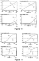
- the I-V measurements between a metal contact 6 and a backside contact 20 of the Ge substrate 1 are shown in Figure 10.
- Figure 10(a) shows I-V measurements for Al/GeN/Ge (curve 21) and Al/Ge (curve 22), Figure 10(b) for Cr/GeN/Ge (curve 21) and Cr/Ge (curve 22), Figure 10(c) for Au/GeN/Ge (curve 21) and Au/Ge (curve 22) and Figure 10(d) for Pt/GeN/Ge (curve 21) and Pt/Ge (curve 22).
- Al and Cr contacts show rectifying behaviour when formed directly onto a bare Ge surface but show Ohmic behaviour when formed on a nitridated Ge substrate 1, or in other words, when formed on a GeN layer 4 formed by the method according to embodiments of the invention.
- This is also indicated in Table 2 below, where results of the I-V measurements are summarized.
- Table 2 shows the resistance between a 500 ⁇ m diameter contact 6 and a backside contact 20 of the Ge substrate 1 at -1V (needle on the 500 ⁇ m contact is at -1 V, the chuck is grounded) is given, as well as the corresponding current density for the different metals used to form contacts both on bare Ge and on GeN/Ge.
- Table 2 results from I-V measurements using different contacting materials Substrate Ge substrate GeN/Ge substrate measurement IV curve current density resistance IV curve current density resistance Al/Au rectifying 4.5e-3 A/cm 2 Ohmic 3.4 A/cm 2 113083 Ohm 149 Ohm Cr/Au rectifying 3.03E-2 A/cm 2 Ohmic 4.5 A/cm 2 16827 Ohm 114 Ohm Au/Au rectifying 4.6e-3 A/cm 2 rectifying 4.6e-2 A/cm 2 109754 Ohm 10989 Ohm Pt/Au rectifying 4.1e-3 A/cm 2 rectifying 2.8e-2 A/cm 2 124780 Ohm 18455 Ohm
- I-V measurements were also performed between two metal contacts 6, 7 (see experimental set-up as illustrated in Figure 9(b) ). The results of these I-V measurements are shown in Figure 11.
- Figure 11(a) shows I-V measurements for Al/GeN/Ge (curve 23) and Al/Ge (curve 24)
- Figure 10(b) for Cr/GeN/Ge (curve 23) and Cr/Ge (curve 24)
- Figure 10(d) for Pt/GeN/Ge (curve 23) and Pt/Ge (curve 24).
- the resistance determined at 0.5 V is shown in Table 4 below.
- AuGe/Ni/Au contacts on Ge the following processing steps were performed.
- a n-type Ge(111) substrate 1 with a carrier concentration of 8e15-8e16 carriers/cm 3 was dipped in water to remove native Ge oxide.
- a metal stack comprising AuGe/Ni/Au was deposited through a shadow mask followed by annealing at 380°C in forming (N 2 /H 2 ) gas. Annealing of this metal stack mixes the different materials and lets them diffuse into the Ge substrate. This lowers the contact resistance.
- Ni For contacting Ge with Ni, processing was done as follows. Another n-type Ge(111) substrate 1 with a carrier concentration of 8e15-8e16 carriers/cm 3 was also dipped in water to remove native Ge oxide. Subsequently, Ni was deposited through a shadow mask followed by annealing at 350 °C in nitrogen. As Ni has a higher workfunction (5.15 eV) than the electron affinity of Ge (4.0 eV), the contact formed would be expected to show Schottky behaviour on n-Ge in the absence of surface traps at the Ge surface. Annealing leads to formation of NiGe, which lowers the contact resistance.
- I-V measurements were done on both samples between metal contacts, i.e. respectively the AuGe/Ni/Au contacts and the Ni contacts, on the Ge substrate 1 and a backside contact of the Ge substrate 1 at -1V.
- the resistance of the AuGe/Ni/Au and Ni contacts was then compared to the resistance of a 20 nm thick Al contact with 100nm Au on top on a bare Ge substrate 1 and on GeN/Ge substrate according to the processing described above (see experiment 4). The results are summarized in Table 5.
- Table 5 Current density between a metal contact and a backside contact of the Ge substrate at -1 V Metal Substrate Current density Al Ge/GeN 3.4 A/cm2 Al Ge 4.5e-3 A/cm2 AuGe/Ni/Au with anneal Ge 4.0e-2A/cm2 Ni with anneal Ge 2.2e-3 A/cm2
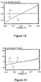
- FIG. 12 shows results of an I-V measurement between a top contact 6 and a backside contact 20 on the Ge substrate 1.
- Curve 28 shows I-V measurements for an Al/GeN/Ge contact, curve 29 for a Ni/Ge contact after anneal and curve 30 for an AuGe/Ni/Au/Ge contact after anneal.
- a monocrystalline GeN layer 4 formed by the method according to embodiments of the present invention on an n-Ge(111) substrate 1 provides high current densities of 3.4 A/cm2 and thus low contact resistance.
- the current density obtained at Al/n-GeN/Ge contacts is much higher than for Al contacts on bare Ge substrates or AuGe/Ni/Au contacts and the Ni contacts used in prior art for lowering contact resistance (see Table 5).
- Ohmic or low resistance contacts can be formed by first forming a GeN layer 4 on the Ge substrate 1 with the method according to embodiments of the present invention before forming the contacts. This may be more easy and cheaper than the requirement to form AuGe/Ni/Au contacts.
- an n-type Ge(111) substrate 1 was nitridated at high temperature of between 700°C and 800°C to form a thin monocrystalline GeN layer 4 on the substrate 1.
- the existence of this GeN layer 4 was confirmed by RHEED measurements and by spectroscopic ellipsometry.
- the sample was dipped into a 2 % HF solution for 1 minute. Spectroscopic ellipsometry showed the removal of the GeN layer 4 after this dip.
- the sample was then loaded into a UHV system.
- the sample was annealed for 10 minutes at ⁇ 350°C, to degas the sample.
- RHEED measurements indicated the removal of the GeN layer 4 and showed a nice reconstructed Ge surface.
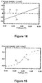
- Figure 14 shows results of I-V measurements between two 500 ⁇ m diameter contacts 6, 7.
- Curve 34 shows I-V measurements for Al/GeN/Ge contacts, curve 35 for Al/Ge for which GeN was removed by HF and curve 36 for Al/Ge contacts.
- Figure 15 shows a zoom of the I-V measurements between two 500 mm diameter contacts 6, 7 as shown in Figure 14 for the Al/Ge contacts (curve 32) and for Al/Ge for which GeN was removed by HF (curve 33). This shows the thin GeN layer 4 is responsible for lowering the contact resistance and not a doping effect of nitrogen into the Ge.
- a GaN layer 5 was grown onto a GeN/Ge(111) substrate and the crystal quality of this GaN layer 5 was studied.
- a Ge(111) substrate 1 was cleaned to remove, for example, oxides and/or organic materials which may be present at the surface of the substrate 1. Cleaning was done by chemical cleaning. After cleaning, the Ge(111) substrate 1 was loaded in the MBE system and outgassed while it was heated to about 550°C.
- the Ge surface 3 of the substrate 1 Prior to growth of the GaN layer 5, the Ge surface 3 of the substrate 1 was exposed to a nitrogen gas flow at a nitridation temperature between 650°C and 750°C, in that way forming a thin GeN layer 4 which then enables crystalline growth of the GaN layer 5.
- GaN was deposited by providing a Ga source flow next to the nitrogen gas flow at different deposition temperatures between 550°C and 800°C for different experiments, in order to determine optimal growth conditions.
- the nitrogen source for the nitrogen gas flow may, according to the present example, be formed by a nitrogen plasma.
- the nitrogen gas flow and the Ga flux may preferably have a comparable atomic flux.
- the pressure in the deposition chamber was in the order of 10 -5 Torr.
- the deposition rate was in the order of 180 to 690 nm/h.
- Different GaN layers 5 with thicknesses between 1.5 nm en 450 nm were deposited.
- the surface morphology and crystal quality of the different GaN layers 5 have been studied RHEED.
- the grown GaN layers 5 were then afterwards studied with XRD omega-2theta scan and omega scan.
- a thin GaN layer 5 of ⁇ 10 nm was deposited or grown at a deposition temperature of 550°C.
- a thicker GaN layer of ⁇ 310 nm was deposited at a higher temperature of 750°C.
- a thin GaN layer of ⁇ 35 nm was deposited at a temperature of 750°C.
- a thicker GaN layer of ⁇ 290 nm was deposited at different temperatures below the deposition temperature of the thin GaN layer, i.e. at ⁇ 550°C, ⁇ 620°C and ⁇ 690°C.
- Growth at a temperature of ⁇ 800°C i.e. above the temperature of the thin GaN layer was also performed but the crystal quality of the resulting layer was not better than for the sample grown at 750°C.
- the RHEED diffraction pattern showed a smooth transition from Ge streaks towards GaN streaks in a few tens of seconds. During the transition no roughening of the surface is observed. The RHEED streaks stay smooth and do not show spots, indicating a smooth surface. This indicates that the GaN lattice fits well on top of the Ge crystal. This is because of the presence of the thin GeN layer 4, which may preferably only be 1 to 2 monolayers thick. The distance between the main streaks visible in the RHEED diffraction pattern does not change when the Ge is nitridated. This indicates that the GeN layer 4 that is formed has the same in-plane lattice parameters as the Ge of the substrate 1 underneath. This result is in contradiction with expectations based on the theoretical lattice mismatch between GaN and Ge being -20.3%. From this large lattice mismatch, roughening would be expected to be seen during RHEED experiments at the start of GaN growth.
- the distance of the RHEED streaks changes abruptly at the start of GaN growth. From an analysis of the distance between the streaks of GaN and the Ge lattice, an in-plane lattice parameter of 3.20 ( ⁇ 0.02) ⁇ could be extracted in case of a thin GaN layer 5 of about 40 nm grown on top of the substrate 1. This indicates that the GaN is not stressed and that the GaN grows relaxated from the beginning. This is a good sign because defects occur when a layer is stressed in order to relieve that stress.
- Table 6 results with respect to the crystal quality are shown for a thin layer of 38 nm of GaN on Ge(111).
- Table 6 Experimental results for a 38 nm thick GaN layer on a Ge(111) substrate. Growth Integrated peak intensity FWHM ⁇ FWHM ⁇ /2 ⁇ FWHM ⁇ /2 ⁇ Thickness GaN GaN GaN Ge GaN (%) (s) (s) (s) nm sample 2.1 371 396 58 38
- an XRD FWHM value of the omega scan was determined to be only 371 arcseconds (see Figure 16 ), which is very good considering the small thickness of this layer 5.
- Thin layer fringes are visible in the omega-2theta scan (see Figure 17 ).
- the presence of such fringes 25, also referred to as Kiessig fringes, are indicative for a good interface quality between the GaN layer 5 (indicated by peak 26) and the Ge substrate 1 (indicated by peak 27).
- the GeN layer 4 is, as already discussed before, preferably not much thicker than a few monolayers and forms a natural transition between Ge and GaN, but is too thin to be observed in XRD experiments.
- the GaN layer 5 formed according to the present example has a crystal quality which is comparable to or better than the crystal quality of GaN grown or deposited on a Si substrate with at least one intermediate layer in between the GaN and the substrate and which is comparable to the crystal quality obtained for GaN on Sapphire substrates with at least one intermediate layer (low quality GaN layer grown at low temperature) in between the good quality GaN and the substrate.
- For GaN on Sapphire average values for the XRD omega scan of 300 arcseconds are obtained and for GaN on Si average values for the XRD omega scan of 600 arcseconds are obtained for thick GaN layers, i.e. for GaN layers 5 with a thickness of higher than 1 micron (see earlier). For thin layers no other substrate can compare to Ge to grow GaN on.
- Thin layers such as the 40 nm thick GaN layer 5 of the present example, cannot be grown on Si, Sapphire or SiC with such good quality as is obtained with the method according to embodiments of the present invention for GaN on Ge. For thicker layers, Sapphire gives better quality.
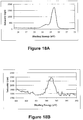
- X-ray Photoelectron Spectroscopy (XPS) measurements performed on a nitridated Ge substrate formed according to the first example show a peak for Ge (see Figure 18A ) and GeN (see Figure 18B ).
- the second, small peak in Figure 18A just before the Ge peak may be due to a Ge-nitride binding.
- Figure 18B proves that this second, small peak is due to a nitride binding because the binding energy coincides with reference nitride binding energy (for WN, BN and NaSCN), which lies between 397 and 398 eV as can be seen from Figure 18B.
- Figure 18A shows a large peak that is due to the Ge substrate (Ge-Ge binding).
- the small peak in Figure 18A is due to the binding of Ge and another element.
- Figure 18B shows the peak due to the binding of nitrogen with another element. This shows that the small peak in figure 18A is due to the binding of Ge and N.
- the peak of the binding of an element, for example Ge shifts very slightly when it binds with another element. So the peak of Ge bound with N is a little shifted with respect to the peak of Ge bound with Ge.
- the size of the peak is indicative for the thickness of the GeN layer. So from the small peak the thickness of the GeN can be estimated.
- a thickness of 0.7 nm is found.
- the measurements illustrated in Figure 7A and 7B indicate the formation of a GeN layer 4 in between the Ge substrate 1 and the GaN layer 5.
- SIMS results for a 450 nm thick GaN layer 5 on a Ge substrate 1 showed limited diffusion of Ga atoms into the Ge substrate 1 and Ge atoms into the GaN layer 5.
- the best layer quality for GaN layers 5 deposited onto a GeN/Ge substrate may be obtained for thin layers of ⁇ 50 nm or less.
- the quality may be slightly reduced, but is still good. This may be due to the fact that when the GaN layer 5 becomes thicker the surface temperature may change because the GaN differently absorbs heat than the Ge substrate 1 and also the heat conduction may be different. Hence, during growth the surface temperature may change and therefore, optimal required growth parameters may change as well.
- an InN layer has been grown on the structure similar to the one obtained in experiment 9, or in other words, an InN layer has been grown on top of a GaN/GeN/Ge structure.
- the GaN layer 5 has a thickness of 5 nm and the InN layer on top of the GaN layer 5 has a thickness of 50 nm.
- An omega/2theta FWHM of 839 arcseconds and a omega scan FWHM of 903 arcseconds were measured.
- the rocking curve value is much smaller than reported before for InN on Ge substrates, which means that the InN layer deposited on the GaN layer has a good crystal quality.
- the omega/2theta scan no GeN peak was observed. This is because the GeN layer is preferably only 1 or 2 monolayers thick and can be considered as a binding or transition between two materials, i.e. Ge and GaN, and should, when it is only 1 or 2 monolayers thick.
- Nitridation prior to growth of InN leads to crystalline InN whereas the process without a nitridation step and thus without formation of a GeN layer 4 in between the substrate 1 and the InN layer, leads to amorphous (non-crystalline) InN. This is confirmed by the absence of an InN peak in the omega/2theta scan.
- an AlGaN layer comprising ⁇ 8% Al and ⁇ 92% Ga was formed on a GeN/Ge substrate at a temperature of ⁇ 750°C.
- the quality of the AlGaN in this case is found to be slightly less than that of GaN layers of comparable thickness, but is still very good.
- the AlGaN peak moved a little bit to the right when compared to pure GaN because of the extra Al present in the alloy. From this experiment it can be concluded that high quality AlGaN can be grown on a GeN/Ge substrate formed with the method according to embodiments of the present invention.
Landscapes
- Chemical & Material Sciences (AREA)
- Engineering & Computer Science (AREA)
- Crystallography & Structural Chemistry (AREA)
- Materials Engineering (AREA)
- Metallurgy (AREA)
- Organic Chemistry (AREA)
- Inorganic Chemistry (AREA)
- Crystals, And After-Treatments Of Crystals (AREA)
- Electrodes Of Semiconductors (AREA)
- Recrystallisation Techniques (AREA)
- Physical Vapour Deposition (AREA)
- Led Devices (AREA)
- Physical Deposition Of Substances That Are Components Of Semiconductor Devices (AREA)
- Chemical Vapour Deposition (AREA)
- Internal Circuitry In Semiconductor Integrated Circuit Devices (AREA)
- Bipolar Transistors (AREA)
Claims (24)
- Procédé de formation d'une couche de GeN monocristalline (4) sur un substrat (1), le substrat (1) comprenant au moins une surface de Ge (3), dans lequel le procédé comprend :- tout en chauffant le substrat (1) à une température comprise entre 650 °C et 940 °C, l'exposition du substrat (1) à un flux de gaz azote, formant de la sorte une couche de GeN monocristalline (4) ;- le refroidissement du substrat (1) à une température inférieure à 650 °C après formation de ladite couche de GeN monocristalline (4) ; et- le maintien du flux de gaz azote au cours du refroidissement du substrat pour entretenir ladite couche de GeN monocristalline (4) ;dans lequel ladite surface de Ge (3) a une orientation (111) ou a une chute entre 0° et 15° et dans lequel le procédé comprend l'application d'un plasma tout en exposant le substrat (1) au flux de gaz azote.
- Procédé selon la revendication 1, dans lequel le substrat (1) comprend au moins une surface de Ge (3) avec une structure hexagonale.
- Procédé selon l'une quelconque des revendications précédentes, dans lequel l'exposition du substrat (1) à un flux de gaz azote est effectuée en exposant le substrat (1) à un flux de gaz azote comprenant du N2 ou du NH3.
- Procédé selon l'une quelconque des revendications précédentes, comprenant la croissance de la couche de GeN monocristalline (4) jusqu'à une épaisseur comprise entre 0,1 nm et 100 nm.
- Procédé selon l'une quelconque des revendications précédentes, dans lequel la surface de Ge (3) est réorganisée lors du chauffage du substrat (1).
- Procédé selon l'une quelconque des revendications précédentes, comprenant en outre une configuration de motifs sur la couche de GeN (4).
- Procédé selon l'une quelconque des revendications précédentes, comprenant en outre le nettoyage de ladite surface de Ge (3) avant d'exposer le substrat (1) à un flux de gaz azote.
- Procédé de formation de contacts métalliques (6, 7) sur un substrat (1), le procédé comprenant :- la formation d'une couche de GeN monocristalline (4) sur un substrat (1) comprenant au moins une surface de Ge (3) en utilisant le procédé selon l'une quelconque des revendications 1 à 7, ladite couche de GeN monocristalline (4) ayant une épaisseur comprise entre 0,1 et 2 nm et- la formation de contacts métalliques (6, 7) sur la couche de GeN monocristalline (4).
- Procédé selon la revendication 8, dans lequel la formation de contacts métalliques (6, 7) sur la couche de GeN monocristalline (4) est effectuée de sorte que les contacts métalliques (6, 7) soient des contacts ohmiques.
- Procédé selon la revendication 8, dans lequel la formation de contacts métalliques (6, 7) sur la couche de GeN monocristalline (4) est effectuée de sorte que les contacts métalliques (6, 7) soient des contacts de Schottky.
- Procédé de formation d'au moins une couche de nitrure du groupe III sur un substrat (1) comprenant :- la formation d'une couche de GeN monocristalline (4) sur un substrat (1) comprenant au moins une surface de Ge (3) en utilisant le procédé selon l'une quelconque des revendications 1 à 7, et- la formation d'au moins une couche de nitrure du groupe III sur la couche de GeN (4).
- Procédé selon la revendication 11, dans lequel la formation d'au moins une couche de nitrure du groupe III sur la couche de GeN (4) est effectuée en déposant au moins une couche de nitrure du groupe III à une température de dépôt comprise entre 550 °C et 850 °C.
- Procédé selon la revendication 11 ou 12, comprenant en outre la configuration de motifs sur au moins l'une de la au moins une couche de nitrure du groupe III.
- Structure comprenant :- un substrat (1) comprenant au moins une surface de Ge (3) ayant une orientation (111) ou ayant une chute entre 0° et 15°,- une couche de GeN monocristalline (4) par-dessus la surface de Ge (3) du substrat (1) et en contact direct avec celle-ci.
- Structure selon la revendication 14, dans laquelle la surface de Ge (3) a une symétrie hexagonale.
- Structure selon l'une quelconque des revendications 14 à 15, dans laquelle la couche de GeN monocristalline (4) a une épaisseur comprise entre 0,1 nm et 100 nm.
- Structure selon l'une quelconque des revendications 14 à 16, dans laquelle la couche de GeN monocristalline (4) est configurée avec des motifs.
- Structure selon l'une quelconque des revendications 14 à 16, dans laquelle la couche de GeN monocristalline (4) a une épaisseur comprise entre 0,1 nm et 2 nm et la structure comprend en outre des contacts métalliques (6, 7) en contact direct avec la couche de GeN monocristalline (4).
- Structure selon la revendication 18, dans laquelle lesdits contacts sont des contacts ohmiques.
- Structure selon la revendication 18, dans laquelle lesdits contacts sont des contacts de Schottky.
- Structure selon l'une quelconque des revendications 14 à 20, comprenant en outre au moins une couche isolante par-dessus la couche de GeN (4).
- Structure selon la revendication 21, dans laquelle la au moins une couche isolante est choisie dans le groupe constitué de SiN, de SiO, de HfO et de matériaux organiques.
- Structure selon l'une quelconque des revendications 14 à 22, dans laquelle la structure comprend en outre au moins une couche de nitrure du groupe III sur la couche de GeN monocristalline (4).
- Structure selon la revendication 23, dans laquelle au moins l'une de la au moins une couche de nitrure de groupe III est configurée avec des motifs.
Priority Applications (1)
| Application Number | Priority Date | Filing Date | Title |
|---|---|---|---|
| EP07784904.0A EP2050126B1 (fr) | 2006-07-27 | 2007-07-20 | FORMATION DE GeN MONOCRISTALLIN SUR UN SUBSTRAT |
Applications Claiming Priority (4)
| Application Number | Priority Date | Filing Date | Title |
|---|---|---|---|
| US83425706P | 2006-07-27 | 2006-07-27 | |
| EP07005755A EP1883103A3 (fr) | 2006-07-27 | 2007-03-21 | Dépôt de nitrures de groupe III sur du Ge |
| PCT/BE2007/000087 WO2008011688A2 (fr) | 2006-07-27 | 2007-07-20 | FORMATION DE GeN MONOCRISTALLIN SUR UN SUBSTRAT |
| EP07784904.0A EP2050126B1 (fr) | 2006-07-27 | 2007-07-20 | FORMATION DE GeN MONOCRISTALLIN SUR UN SUBSTRAT |
Publications (2)
| Publication Number | Publication Date |
|---|---|
| EP2050126A2 EP2050126A2 (fr) | 2009-04-22 |
| EP2050126B1 true EP2050126B1 (fr) | 2019-03-20 |
Family
ID=38042784
Family Applications (3)
| Application Number | Title | Priority Date | Filing Date |
|---|---|---|---|
| EP07005755A Withdrawn EP1883103A3 (fr) | 2006-07-27 | 2007-03-21 | Dépôt de nitrures de groupe III sur du Ge |
| EP07765130A Withdrawn EP2047501A1 (fr) | 2006-07-27 | 2007-07-09 | Dépôt de nitrures du groupe iii sur ge |
| EP07784904.0A Active EP2050126B1 (fr) | 2006-07-27 | 2007-07-20 | FORMATION DE GeN MONOCRISTALLIN SUR UN SUBSTRAT |
Family Applications Before (2)
| Application Number | Title | Priority Date | Filing Date |
|---|---|---|---|
| EP07005755A Withdrawn EP1883103A3 (fr) | 2006-07-27 | 2007-03-21 | Dépôt de nitrures de groupe III sur du Ge |
| EP07765130A Withdrawn EP2047501A1 (fr) | 2006-07-27 | 2007-07-09 | Dépôt de nitrures du groupe iii sur ge |
Country Status (4)
| Country | Link |
|---|---|
| US (2) | US7964482B2 (fr) |
| EP (3) | EP1883103A3 (fr) |
| JP (3) | JP4917152B2 (fr) |
| WO (3) | WO2008011979A1 (fr) |
Families Citing this family (23)
| Publication number | Priority date | Publication date | Assignee | Title |
|---|---|---|---|---|
| EP1130091A3 (fr) | 2000-03-01 | 2001-11-14 | Message Pharmaceuticals, Inc. | Protéines de RNase P d'origine bactérienne et leur utilisation pour identifier des composés antibactériens |
| KR100661602B1 (ko) * | 2005-12-09 | 2006-12-26 | 삼성전기주식회사 | 수직 구조 질화갈륨계 led 소자의 제조방법 |
| DE102008027131A1 (de) | 2008-05-30 | 2009-12-03 | Picanol N.V. | Vorrichtung zum Trennen eines Schussfadens |
| DE102008027140A1 (de) | 2008-05-30 | 2009-12-03 | Picanol N.V. | Vorrichtung und Verfahren zum Schneiden eines einzutragenden Schussfadens |
| EP2270840B1 (fr) * | 2009-06-29 | 2020-06-03 | IMEC vzw | Procédé de fabrication d'un substrat en materiau III-V et substrat correspondant |
| US8274116B2 (en) * | 2009-11-16 | 2012-09-25 | International Business Machines Corporation | Control of threshold voltages in high-k metal gate stack and structures for CMOS devices |
| US8178443B2 (en) * | 2009-12-04 | 2012-05-15 | Novellus Systems, Inc. | Hardmask materials |
| KR101431168B1 (ko) * | 2010-06-25 | 2014-08-18 | 가부시키가이샤 아루박 | 성막 장치, 성막 장치의 유지보수 방법 |
| JP2012015304A (ja) * | 2010-06-30 | 2012-01-19 | Sumitomo Electric Ind Ltd | 半導体装置 |
| EP2461352B1 (fr) * | 2010-12-06 | 2013-07-10 | Imec | Procédé de fabrication de contacts à faible résistance sur germanium de type n |
| WO2013063038A1 (fr) * | 2011-10-24 | 2013-05-02 | Rosestreet Labs, Llc | Détecteurs de lumière uv à base de nitrure sur substrats en silicium |
| US8878251B2 (en) * | 2012-10-17 | 2014-11-04 | Seoul National University R&Db Foundation | Silicon-compatible compound junctionless field effect transistor |
| US9214630B2 (en) * | 2013-04-11 | 2015-12-15 | Air Products And Chemicals, Inc. | Method of making a multicomponent film |
| JP2014220274A (ja) * | 2013-05-01 | 2014-11-20 | 株式会社東芝 | 半導体装置及びその製造方法 |
| US9368582B2 (en) | 2013-11-04 | 2016-06-14 | Avogy, Inc. | High power gallium nitride electronics using miscut substrates |
| US9460917B2 (en) * | 2014-02-12 | 2016-10-04 | Translucent, Inc. | Method of growing III-N semiconductor layer on Si substrate |
| KR20160025781A (ko) | 2014-08-28 | 2016-03-09 | 전북대학교산학협력단 | 반도체 소자 및 제조방법 |
| US10269565B2 (en) * | 2015-01-09 | 2019-04-23 | Swegan Ab | Semiconductor device structure and methods of its production |
| WO2016155794A1 (fr) | 2015-03-31 | 2016-10-06 | Erik Janzén | Hétérostructure et son procédé de production |
| US9917156B1 (en) | 2016-09-02 | 2018-03-13 | IQE, plc | Nucleation layer for growth of III-nitride structures |
| WO2019066825A1 (fr) * | 2017-09-27 | 2019-04-04 | Intel Corporation | Couche de passivation pour substrat en germanium |
| CN113838929B (zh) * | 2020-06-23 | 2025-10-17 | 广东致能半导体有限公司 | 一种半导体器件及其制造方法 |
| CN111893566A (zh) * | 2020-07-21 | 2020-11-06 | 璨隆科技发展有限公司 | 一种氮化镓晶体的制备方法 |
Family Cites Families (25)
| Publication number | Priority date | Publication date | Assignee | Title |
|---|---|---|---|---|
| US4254429A (en) * | 1978-07-08 | 1981-03-03 | Shunpei Yamazaki | Hetero junction semiconductor device |
| US4514748A (en) * | 1983-11-21 | 1985-04-30 | At&T Bell Laboratories | Germanium p-i-n photodetector on silicon substrate |
| US4671845A (en) | 1985-03-22 | 1987-06-09 | The United States Of America As Represented By The Secretary Of The Navy | Method for producing high quality germanium-germanium nitride interfaces for germanium semiconductors and device produced thereby |
| JPS62231202A (ja) * | 1986-03-31 | 1987-10-09 | Nec Corp | 分光器用結晶、量子細線構造及びそれらの製造方法 |
| JPH0594874A (ja) * | 1991-06-26 | 1993-04-16 | Ricoh Co Ltd | 能動素子 |
| US5357122A (en) * | 1991-09-05 | 1994-10-18 | Sony Corporation | Three-dimensional optical-electronic integrated circuit device with raised sections |
| DE69622277T2 (de) * | 1995-09-18 | 2003-03-27 | Hitachi, Ltd. | Halbleitermaterial, verfahren zur herstellung des halbleitermaterials und eine halbleitervorrichtung |
| JPH10242586A (ja) * | 1997-02-24 | 1998-09-11 | Fuji Electric Co Ltd | Iii 族窒化物半導体装置およびその製造方法 |
| JPH10303510A (ja) * | 1997-04-23 | 1998-11-13 | Fuji Electric Co Ltd | Iii 族窒化物半導体素子およびその製造方法 |
| JPH11346002A (ja) * | 1998-04-01 | 1999-12-14 | Matsushita Electric Ind Co Ltd | p型窒化ガリウム系化合物半導体の製造方法 |
| JP2000353809A (ja) * | 1999-03-02 | 2000-12-19 | Semiconductor Energy Lab Co Ltd | 半導体装置およびその作製方法 |
| JP4282173B2 (ja) * | 1999-09-03 | 2009-06-17 | シャープ株式会社 | 窒素化合物半導体発光素子およびその製造方法 |
| JP2002145700A (ja) * | 2000-08-14 | 2002-05-22 | Nippon Telegr & Teleph Corp <Ntt> | サファイア基板および半導体素子ならびに電子部品および結晶成長方法 |
| JP2002241198A (ja) * | 2001-02-13 | 2002-08-28 | Hitachi Cable Ltd | GaN単結晶基板及びその製造方法 |
| FR2836159B1 (fr) * | 2002-02-15 | 2004-05-07 | Centre Nat Rech Scient | Procede de formation de couche de carbure de silicium ou de nitrure d'element iii sur un substrat adapte |
| US7176483B2 (en) * | 2002-08-12 | 2007-02-13 | Acorn Technologies, Inc. | Method for depinning the Fermi level of a semiconductor at an electrical junction and devices incorporating such junctions |
| GB2398672A (en) * | 2003-02-19 | 2004-08-25 | Qinetiq Ltd | Group IIIA nitride buffer layers |
| WO2005017963A2 (fr) * | 2003-08-04 | 2005-02-24 | Asm America, Inc. | Preparation de surfaces prealable au depot sur germanium |
| EP1583139A1 (fr) * | 2004-04-02 | 2005-10-05 | Interuniversitaire Microelectronica Centrum vzw ( IMEC) | Méthode de dépôt d'un matériau nitrure du groupe III sur un substrat de silicium et dispositif correspondant |
| JP5259914B2 (ja) * | 2003-12-22 | 2013-08-07 | アイメック | シリコン基板上にiii族窒化物材料を成長させた装置及びその作製方法 |
| EP1548807B1 (fr) * | 2003-12-22 | 2018-08-22 | IMEC vzw | Méthode de dépôt d'un matériau nitrure du groupe III sur un substrat de silicium et dispositif correspondant |
| JP3888374B2 (ja) * | 2004-03-17 | 2007-02-28 | 住友電気工業株式会社 | GaN単結晶基板の製造方法 |
| JP4691911B2 (ja) * | 2004-06-11 | 2011-06-01 | 日立電線株式会社 | Iii−v族窒化物系半導体自立基板の製造方法 |
| US7339205B2 (en) * | 2004-06-28 | 2008-03-04 | Nitronex Corporation | Gallium nitride materials and methods associated with the same |
| US20080001181A1 (en) * | 2006-06-28 | 2008-01-03 | Titash Rakshit | Complementarily doped metal-semiconductor interfaces to reduce dark current in MSM photodetectors |
-
2007
- 2007-03-21 EP EP07005755A patent/EP1883103A3/fr not_active Withdrawn
- 2007-07-09 JP JP2009521133A patent/JP4917152B2/ja not_active Expired - Fee Related
- 2007-07-09 EP EP07765130A patent/EP2047501A1/fr not_active Withdrawn
- 2007-07-09 WO PCT/EP2007/006050 patent/WO2008011979A1/fr not_active Ceased
- 2007-07-09 US US12/309,939 patent/US7964482B2/en not_active Expired - Fee Related
- 2007-07-20 JP JP2009521071A patent/JP5204105B2/ja active Active
- 2007-07-20 WO PCT/BE2007/000087 patent/WO2008011688A2/fr not_active Ceased
- 2007-07-20 EP EP07784904.0A patent/EP2050126B1/fr active Active
- 2007-07-20 WO PCT/BE2007/000086 patent/WO2008011687A2/fr not_active Ceased
- 2007-07-20 US US12/309,940 patent/US8017509B2/en active Active
-
2012
- 2012-01-25 JP JP2012012665A patent/JP2012116751A/ja active Pending
Non-Patent Citations (1)
| Title |
|---|
| None * |
Also Published As
| Publication number | Publication date |
|---|---|
| WO2008011688A2 (fr) | 2008-01-31 |
| EP2050126A2 (fr) | 2009-04-22 |
| JP2009545140A (ja) | 2009-12-17 |
| US8017509B2 (en) | 2011-09-13 |
| EP1883103A2 (fr) | 2008-01-30 |
| WO2008011979A1 (fr) | 2008-01-31 |
| JP5204105B2 (ja) | 2013-06-05 |
| WO2008011687A2 (fr) | 2008-01-31 |
| US7964482B2 (en) | 2011-06-21 |
| US20090189192A1 (en) | 2009-07-30 |
| JP2009545145A (ja) | 2009-12-17 |
| WO2008011688A3 (fr) | 2008-03-13 |
| US20110089520A1 (en) | 2011-04-21 |
| EP1883103A3 (fr) | 2008-03-05 |
| EP2047501A1 (fr) | 2009-04-15 |
| JP4917152B2 (ja) | 2012-04-18 |
| JP2012116751A (ja) | 2012-06-21 |
| WO2008011687A3 (fr) | 2008-03-13 |
Similar Documents
| Publication | Publication Date | Title |
|---|---|---|
| EP2050126B1 (fr) | FORMATION DE GeN MONOCRISTALLIN SUR UN SUBSTRAT | |
| US11056569B2 (en) | Method for depinning the fermi level of a semiconductor at an electrical junction and devices incorporating such junctions | |
| US10541315B2 (en) | INP-based transistor fabrication | |
| Hashizume et al. | Chemistry and electrical properties of surfaces of GaN and GaN/AlGaN heterostructures | |
| US9112035B2 (en) | Semiconductor substrate, field-effect transistor, integrated circuit, and method for fabricating semiconductor substrate | |
| EP0964453A2 (fr) | Dispositif comprenant une couche d'oxyde sur un corps semi-conducteur à base de GaAs et sa methode de fabrication | |
| US20050093027A1 (en) | Method for depinning the fermi level of a semiconductor at an electrical junction and devices incorporating such junctions | |
| Li et al. | Material and Device Characteristics of Metamorphic ${\rm In} _ {0.53}{\rm Ga} _ {0.47}{\rm As} $ MOSHEMTs Grown on GaAs and Si Substrates by MOCVD | |
| US20070138506A1 (en) | Nitride metal oxide semiconductor integrated transistor devices | |
| Nguyen et al. | Investigating FinFET sidewall passivation using epitaxial (100) Ge and (110) Ge metal–oxide–semiconductor devices on AlAs/GaAs | |
| US20250167005A1 (en) | Method for manufacturing a substrate wafer for building group iii-v devices thereon and a substrate wafer for building group iii-v devices thereon | |
| Gila et al. | MBE Growth of Oxides for III–N MOSFETs | |
| Gila et al. | A comparison of gallium gadolinium oxide and gadolinium oxide for use as dielectrics in GaN MOSFETs | |
| Abernathy et al. | University of Florida, Gainesville, FL 32606, USA | |
| Abernathy et al. | FABRICATION AND PERFORMANCE OF GaN MOSFETS AND MOSHFETS | |
| Gila et al. | Gadolinium Oxide Gate Dielectrics for GaN MOSFETs | |
| JPH07254708A (ja) | 半導体装置の製造方法 | |
| US20130093029A1 (en) | Process for preparing a beryllium oxide layer on a semiconductor substrate | |
| JPH06334176A (ja) | 半導体装置の製造方法 |
Legal Events
| Date | Code | Title | Description |
|---|---|---|---|
| PUAI | Public reference made under article 153(3) epc to a published international application that has entered the european phase |
Free format text: ORIGINAL CODE: 0009012 |
|
| 17P | Request for examination filed |
Effective date: 20090219 |
|
| AK | Designated contracting states |
Kind code of ref document: A2 Designated state(s): AT BE BG CH CY CZ DE DK EE ES FI FR GB GR HU IE IS IT LI LT LU LV MC MT NL PL PT RO SE SI SK TR |
|
| AX | Request for extension of the european patent |
Extension state: AL BA HR MK RS |
|
| RAP1 | Party data changed (applicant data changed or rights of an application transferred) |
Owner name: VRIJE UNIVERSITEIT BRUSSEL Owner name: IMEC |
|
| DAX | Request for extension of the european patent (deleted) | ||
| 17Q | First examination report despatched |
Effective date: 20120405 |
|
| STAA | Information on the status of an ep patent application or granted ep patent |
Free format text: STATUS: EXAMINATION IS IN PROGRESS |
|
| RAP1 | Party data changed (applicant data changed or rights of an application transferred) |
Owner name: VRIJE UNIVERSITEIT BRUSSEL Owner name: IMEC VZW |
|
| GRAP | Despatch of communication of intention to grant a patent |
Free format text: ORIGINAL CODE: EPIDOSNIGR1 |
|
| STAA | Information on the status of an ep patent application or granted ep patent |
Free format text: STATUS: GRANT OF PATENT IS INTENDED |
|
| GRAJ | Information related to disapproval of communication of intention to grant by the applicant or resumption of examination proceedings by the epo deleted |
Free format text: ORIGINAL CODE: EPIDOSDIGR1 |
|
| GRAJ | Information related to disapproval of communication of intention to grant by the applicant or resumption of examination proceedings by the epo deleted |
Free format text: ORIGINAL CODE: EPIDOSDIGR1 |
|
| GRAP | Despatch of communication of intention to grant a patent |
Free format text: ORIGINAL CODE: EPIDOSNIGR1 |
|
| STAA | Information on the status of an ep patent application or granted ep patent |
Free format text: STATUS: EXAMINATION IS IN PROGRESS |
|
| GRAJ | Information related to disapproval of communication of intention to grant by the applicant or resumption of examination proceedings by the epo deleted |
Free format text: ORIGINAL CODE: EPIDOSDIGR1 |
|
| GRAP | Despatch of communication of intention to grant a patent |
Free format text: ORIGINAL CODE: EPIDOSNIGR1 |
|
| INTG | Intention to grant announced |
Effective date: 20180822 |
|
| INTG | Intention to grant announced |
Effective date: 20180830 |
|
| GRAP | Despatch of communication of intention to grant a patent |
Free format text: ORIGINAL CODE: EPIDOSNIGR1 |
|
| INTC | Intention to grant announced (deleted) | ||
| STAA | Information on the status of an ep patent application or granted ep patent |
Free format text: STATUS: GRANT OF PATENT IS INTENDED |
|
| INTG | Intention to grant announced |
Effective date: 20181004 |
|
| GRAS | Grant fee paid |
Free format text: ORIGINAL CODE: EPIDOSNIGR3 |
|
| GRAA | (expected) grant |
Free format text: ORIGINAL CODE: 0009210 |
|
| STAA | Information on the status of an ep patent application or granted ep patent |
Free format text: STATUS: THE PATENT HAS BEEN GRANTED |
|
| AK | Designated contracting states |
Kind code of ref document: B1 Designated state(s): AT BE BG CH CY CZ DE DK EE ES FI FR GB GR HU IE IS IT LI LT LU LV MC MT NL PL PT RO SE SI SK TR |
|
| REG | Reference to a national code |
Ref country code: GB Ref legal event code: FG4D |
|
| REG | Reference to a national code |
Ref country code: CH Ref legal event code: EP |
|
| REG | Reference to a national code |
Ref country code: DE Ref legal event code: R096 Ref document number: 602007057901 Country of ref document: DE |
|
| REG | Reference to a national code |
Ref country code: AT Ref legal event code: REF Ref document number: 1111372 Country of ref document: AT Kind code of ref document: T Effective date: 20190415 |
|
| REG | Reference to a national code |
Ref country code: IE Ref legal event code: FG4D |
|
| REG | Reference to a national code |
Ref country code: NL Ref legal event code: MP Effective date: 20190320 |
|
| PG25 | Lapsed in a contracting state [announced via postgrant information from national office to epo] |
Ref country code: FI Free format text: LAPSE BECAUSE OF FAILURE TO SUBMIT A TRANSLATION OF THE DESCRIPTION OR TO PAY THE FEE WITHIN THE PRESCRIBED TIME-LIMIT Effective date: 20190320 Ref country code: SE Free format text: LAPSE BECAUSE OF FAILURE TO SUBMIT A TRANSLATION OF THE DESCRIPTION OR TO PAY THE FEE WITHIN THE PRESCRIBED TIME-LIMIT Effective date: 20190320 Ref country code: LT Free format text: LAPSE BECAUSE OF FAILURE TO SUBMIT A TRANSLATION OF THE DESCRIPTION OR TO PAY THE FEE WITHIN THE PRESCRIBED TIME-LIMIT Effective date: 20190320 |
|
| REG | Reference to a national code |
Ref country code: LT Ref legal event code: MG4D |
|
| PG25 | Lapsed in a contracting state [announced via postgrant information from national office to epo] |
Ref country code: LV Free format text: LAPSE BECAUSE OF FAILURE TO SUBMIT A TRANSLATION OF THE DESCRIPTION OR TO PAY THE FEE WITHIN THE PRESCRIBED TIME-LIMIT Effective date: 20190320 Ref country code: NL Free format text: LAPSE BECAUSE OF FAILURE TO SUBMIT A TRANSLATION OF THE DESCRIPTION OR TO PAY THE FEE WITHIN THE PRESCRIBED TIME-LIMIT Effective date: 20190320 Ref country code: GR Free format text: LAPSE BECAUSE OF FAILURE TO SUBMIT A TRANSLATION OF THE DESCRIPTION OR TO PAY THE FEE WITHIN THE PRESCRIBED TIME-LIMIT Effective date: 20190621 Ref country code: BG Free format text: LAPSE BECAUSE OF FAILURE TO SUBMIT A TRANSLATION OF THE DESCRIPTION OR TO PAY THE FEE WITHIN THE PRESCRIBED TIME-LIMIT Effective date: 20190620 |
|
| REG | Reference to a national code |
Ref country code: AT Ref legal event code: MK05 Ref document number: 1111372 Country of ref document: AT Kind code of ref document: T Effective date: 20190320 |
|
| PG25 | Lapsed in a contracting state [announced via postgrant information from national office to epo] |
Ref country code: EE Free format text: LAPSE BECAUSE OF FAILURE TO SUBMIT A TRANSLATION OF THE DESCRIPTION OR TO PAY THE FEE WITHIN THE PRESCRIBED TIME-LIMIT Effective date: 20190320 Ref country code: ES Free format text: LAPSE BECAUSE OF FAILURE TO SUBMIT A TRANSLATION OF THE DESCRIPTION OR TO PAY THE FEE WITHIN THE PRESCRIBED TIME-LIMIT Effective date: 20190320 Ref country code: CZ Free format text: LAPSE BECAUSE OF FAILURE TO SUBMIT A TRANSLATION OF THE DESCRIPTION OR TO PAY THE FEE WITHIN THE PRESCRIBED TIME-LIMIT Effective date: 20190320 Ref country code: RO Free format text: LAPSE BECAUSE OF FAILURE TO SUBMIT A TRANSLATION OF THE DESCRIPTION OR TO PAY THE FEE WITHIN THE PRESCRIBED TIME-LIMIT Effective date: 20190320 Ref country code: IT Free format text: LAPSE BECAUSE OF FAILURE TO SUBMIT A TRANSLATION OF THE DESCRIPTION OR TO PAY THE FEE WITHIN THE PRESCRIBED TIME-LIMIT Effective date: 20190320 Ref country code: SK Free format text: LAPSE BECAUSE OF FAILURE TO SUBMIT A TRANSLATION OF THE DESCRIPTION OR TO PAY THE FEE WITHIN THE PRESCRIBED TIME-LIMIT Effective date: 20190320 Ref country code: PT Free format text: LAPSE BECAUSE OF FAILURE TO SUBMIT A TRANSLATION OF THE DESCRIPTION OR TO PAY THE FEE WITHIN THE PRESCRIBED TIME-LIMIT Effective date: 20190720 |
|
| PG25 | Lapsed in a contracting state [announced via postgrant information from national office to epo] |
Ref country code: PL Free format text: LAPSE BECAUSE OF FAILURE TO SUBMIT A TRANSLATION OF THE DESCRIPTION OR TO PAY THE FEE WITHIN THE PRESCRIBED TIME-LIMIT Effective date: 20190320 |
|
| PG25 | Lapsed in a contracting state [announced via postgrant information from national office to epo] |
Ref country code: AT Free format text: LAPSE BECAUSE OF FAILURE TO SUBMIT A TRANSLATION OF THE DESCRIPTION OR TO PAY THE FEE WITHIN THE PRESCRIBED TIME-LIMIT Effective date: 20190320 Ref country code: IS Free format text: LAPSE BECAUSE OF FAILURE TO SUBMIT A TRANSLATION OF THE DESCRIPTION OR TO PAY THE FEE WITHIN THE PRESCRIBED TIME-LIMIT Effective date: 20190720 |
|
| REG | Reference to a national code |
Ref country code: DE Ref legal event code: R097 Ref document number: 602007057901 Country of ref document: DE |
|
| PLBE | No opposition filed within time limit |
Free format text: ORIGINAL CODE: 0009261 |
|
| STAA | Information on the status of an ep patent application or granted ep patent |
Free format text: STATUS: NO OPPOSITION FILED WITHIN TIME LIMIT |
|
| PG25 | Lapsed in a contracting state [announced via postgrant information from national office to epo] |
Ref country code: DK Free format text: LAPSE BECAUSE OF FAILURE TO SUBMIT A TRANSLATION OF THE DESCRIPTION OR TO PAY THE FEE WITHIN THE PRESCRIBED TIME-LIMIT Effective date: 20190320 |
|
| 26N | No opposition filed |
Effective date: 20200102 |
|
| PG25 | Lapsed in a contracting state [announced via postgrant information from national office to epo] |
Ref country code: SI Free format text: LAPSE BECAUSE OF FAILURE TO SUBMIT A TRANSLATION OF THE DESCRIPTION OR TO PAY THE FEE WITHIN THE PRESCRIBED TIME-LIMIT Effective date: 20190320 Ref country code: MC Free format text: LAPSE BECAUSE OF FAILURE TO SUBMIT A TRANSLATION OF THE DESCRIPTION OR TO PAY THE FEE WITHIN THE PRESCRIBED TIME-LIMIT Effective date: 20190320 |
|
| REG | Reference to a national code |
Ref country code: CH Ref legal event code: PL |
|
| GBPC | Gb: european patent ceased through non-payment of renewal fee |
Effective date: 20190720 |
|
| PG25 | Lapsed in a contracting state [announced via postgrant information from national office to epo] |
Ref country code: TR Free format text: LAPSE BECAUSE OF FAILURE TO SUBMIT A TRANSLATION OF THE DESCRIPTION OR TO PAY THE FEE WITHIN THE PRESCRIBED TIME-LIMIT Effective date: 20190320 |
|
| REG | Reference to a national code |
Ref country code: BE Ref legal event code: MM Effective date: 20190731 |
|
| PG25 | Lapsed in a contracting state [announced via postgrant information from national office to epo] |
Ref country code: GB Free format text: LAPSE BECAUSE OF NON-PAYMENT OF DUE FEES Effective date: 20190720 |
|
| PG25 | Lapsed in a contracting state [announced via postgrant information from national office to epo] |
Ref country code: LI Free format text: LAPSE BECAUSE OF NON-PAYMENT OF DUE FEES Effective date: 20190731 Ref country code: LU Free format text: LAPSE BECAUSE OF NON-PAYMENT OF DUE FEES Effective date: 20190720 Ref country code: BE Free format text: LAPSE BECAUSE OF NON-PAYMENT OF DUE FEES Effective date: 20190731 Ref country code: CH Free format text: LAPSE BECAUSE OF NON-PAYMENT OF DUE FEES Effective date: 20190731 |
|
| PG25 | Lapsed in a contracting state [announced via postgrant information from national office to epo] |
Ref country code: IE Free format text: LAPSE BECAUSE OF NON-PAYMENT OF DUE FEES Effective date: 20190720 |
|
| PG25 | Lapsed in a contracting state [announced via postgrant information from national office to epo] |
Ref country code: CY Free format text: LAPSE BECAUSE OF FAILURE TO SUBMIT A TRANSLATION OF THE DESCRIPTION OR TO PAY THE FEE WITHIN THE PRESCRIBED TIME-LIMIT Effective date: 20190320 |
|
| PG25 | Lapsed in a contracting state [announced via postgrant information from national office to epo] |
Ref country code: MT Free format text: LAPSE BECAUSE OF FAILURE TO SUBMIT A TRANSLATION OF THE DESCRIPTION OR TO PAY THE FEE WITHIN THE PRESCRIBED TIME-LIMIT Effective date: 20190320 Ref country code: HU Free format text: LAPSE BECAUSE OF FAILURE TO SUBMIT A TRANSLATION OF THE DESCRIPTION OR TO PAY THE FEE WITHIN THE PRESCRIBED TIME-LIMIT; INVALID AB INITIO Effective date: 20070720 |
|
| P01 | Opt-out of the competence of the unified patent court (upc) registered |
Effective date: 20230513 |
|
| PGFP | Annual fee paid to national office [announced via postgrant information from national office to epo] |
Ref country code: FR Payment date: 20250620 Year of fee payment: 19 |
|
| PGFP | Annual fee paid to national office [announced via postgrant information from national office to epo] |
Ref country code: DE Payment date: 20250620 Year of fee payment: 19 |
|
| REG | Reference to a national code |
Ref country code: DE Ref legal event code: R079 Ref document number: 602007057901 Country of ref document: DE Free format text: PREVIOUS MAIN CLASS: H01L0021318000 Ipc: H10P0014694000 |