EP2052867A1 - Tête d'impression thermique - Google Patents
Tête d'impression thermique Download PDFInfo
- Publication number
- EP2052867A1 EP2052867A1 EP07791363A EP07791363A EP2052867A1 EP 2052867 A1 EP2052867 A1 EP 2052867A1 EP 07791363 A EP07791363 A EP 07791363A EP 07791363 A EP07791363 A EP 07791363A EP 2052867 A1 EP2052867 A1 EP 2052867A1
- Authority
- EP
- European Patent Office
- Prior art keywords
- thermal conductivity
- layer
- heating resistor
- protective film
- high thermal
- Prior art date
- Legal status (The legal status is an assumption and is not a legal conclusion. Google has not performed a legal analysis and makes no representation as to the accuracy of the status listed.)
- Withdrawn
Links
- 230000001681 protective effect Effects 0.000 claims abstract description 36
- 238000010438 heat treatment Methods 0.000 claims abstract description 32
- 239000000758 substrate Substances 0.000 claims abstract description 17
- 239000000463 material Substances 0.000 claims description 10
- 239000010410 layer Substances 0.000 description 38
- 239000011521 glass Substances 0.000 description 7
- 244000126211 Hericium coralloides Species 0.000 description 3
- 239000011347 resin Substances 0.000 description 2
- 229920005989 resin Polymers 0.000 description 2
- 239000002356 single layer Substances 0.000 description 2
- 238000004544 sputter deposition Methods 0.000 description 2
- PNEYBMLMFCGWSK-UHFFFAOYSA-N Alumina Chemical compound [O-2].[O-2].[O-2].[Al+3].[Al+3] PNEYBMLMFCGWSK-UHFFFAOYSA-N 0.000 description 1
- 230000015572 biosynthetic process Effects 0.000 description 1
- 229910010293 ceramic material Inorganic materials 0.000 description 1
- 238000000034 method Methods 0.000 description 1
- 239000011241 protective layer Substances 0.000 description 1
- 229910001925 ruthenium oxide Inorganic materials 0.000 description 1
- WOCIAKWEIIZHES-UHFFFAOYSA-N ruthenium(iv) oxide Chemical compound O=[Ru]=O WOCIAKWEIIZHES-UHFFFAOYSA-N 0.000 description 1
Images

Classifications
-
- B—PERFORMING OPERATIONS; TRANSPORTING
- B41—PRINTING; LINING MACHINES; TYPEWRITERS; STAMPS
- B41J—TYPEWRITERS; SELECTIVE PRINTING MECHANISMS, i.e. MECHANISMS PRINTING OTHERWISE THAN FROM A FORME; CORRECTION OF TYPOGRAPHICAL ERRORS
- B41J2/00—Typewriters or selective printing mechanisms characterised by the printing or marking process for which they are designed
- B41J2/315—Typewriters or selective printing mechanisms characterised by the printing or marking process for which they are designed characterised by selective application of heat to a heat sensitive printing or impression-transfer material
- B41J2/32—Typewriters or selective printing mechanisms characterised by the printing or marking process for which they are designed characterised by selective application of heat to a heat sensitive printing or impression-transfer material using thermal heads
- B41J2/335—Structure of thermal heads
- B41J2/33505—Constructional details
- B41J2/3351—Electrode layers
-
- B—PERFORMING OPERATIONS; TRANSPORTING
- B41—PRINTING; LINING MACHINES; TYPEWRITERS; STAMPS
- B41J—TYPEWRITERS; SELECTIVE PRINTING MECHANISMS, i.e. MECHANISMS PRINTING OTHERWISE THAN FROM A FORME; CORRECTION OF TYPOGRAPHICAL ERRORS
- B41J2/00—Typewriters or selective printing mechanisms characterised by the printing or marking process for which they are designed
- B41J2/315—Typewriters or selective printing mechanisms characterised by the printing or marking process for which they are designed characterised by selective application of heat to a heat sensitive printing or impression-transfer material
- B41J2/32—Typewriters or selective printing mechanisms characterised by the printing or marking process for which they are designed characterised by selective application of heat to a heat sensitive printing or impression-transfer material using thermal heads
- B41J2/335—Structure of thermal heads
- B41J2/33505—Constructional details
- B41J2/33515—Heater layers
-
- B—PERFORMING OPERATIONS; TRANSPORTING
- B41—PRINTING; LINING MACHINES; TYPEWRITERS; STAMPS
- B41J—TYPEWRITERS; SELECTIVE PRINTING MECHANISMS, i.e. MECHANISMS PRINTING OTHERWISE THAN FROM A FORME; CORRECTION OF TYPOGRAPHICAL ERRORS
- B41J2/00—Typewriters or selective printing mechanisms characterised by the printing or marking process for which they are designed
- B41J2/315—Typewriters or selective printing mechanisms characterised by the printing or marking process for which they are designed characterised by selective application of heat to a heat sensitive printing or impression-transfer material
- B41J2/32—Typewriters or selective printing mechanisms characterised by the printing or marking process for which they are designed characterised by selective application of heat to a heat sensitive printing or impression-transfer material using thermal heads
- B41J2/335—Structure of thermal heads
- B41J2/33505—Constructional details
- B41J2/33525—Passivation layers
-
- B—PERFORMING OPERATIONS; TRANSPORTING
- B41—PRINTING; LINING MACHINES; TYPEWRITERS; STAMPS
- B41J—TYPEWRITERS; SELECTIVE PRINTING MECHANISMS, i.e. MECHANISMS PRINTING OTHERWISE THAN FROM A FORME; CORRECTION OF TYPOGRAPHICAL ERRORS
- B41J2/00—Typewriters or selective printing mechanisms characterised by the printing or marking process for which they are designed
- B41J2/315—Typewriters or selective printing mechanisms characterised by the printing or marking process for which they are designed characterised by selective application of heat to a heat sensitive printing or impression-transfer material
- B41J2/32—Typewriters or selective printing mechanisms characterised by the printing or marking process for which they are designed characterised by selective application of heat to a heat sensitive printing or impression-transfer material using thermal heads
- B41J2/335—Structure of thermal heads
- B41J2/33505—Constructional details
- B41J2/3353—Protective layers
-
- B—PERFORMING OPERATIONS; TRANSPORTING
- B41—PRINTING; LINING MACHINES; TYPEWRITERS; STAMPS
- B41J—TYPEWRITERS; SELECTIVE PRINTING MECHANISMS, i.e. MECHANISMS PRINTING OTHERWISE THAN FROM A FORME; CORRECTION OF TYPOGRAPHICAL ERRORS
- B41J2/00—Typewriters or selective printing mechanisms characterised by the printing or marking process for which they are designed
- B41J2/315—Typewriters or selective printing mechanisms characterised by the printing or marking process for which they are designed characterised by selective application of heat to a heat sensitive printing or impression-transfer material
- B41J2/32—Typewriters or selective printing mechanisms characterised by the printing or marking process for which they are designed characterised by selective application of heat to a heat sensitive printing or impression-transfer material using thermal heads
- B41J2/335—Structure of thermal heads
- B41J2/33555—Structure of thermal heads characterised by type
- B41J2/3357—Surface type resistors
Definitions
- the present invention relates to a thermal printhead incorporated in a thermal printer.
- a thermal printhead includes an insulating substrate and a heating resistor formed on the substrate. In printing, current is applied to the heating resistor, whereby images or letters are formed on a recording medium such as thermal paper (see Patent Document 1 below).
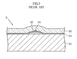
- Fig. 5 is a partial sectional view showing an example of conventional thermal printhead.
- the thermal printhead X shown in the figure includes a substrate 91 and a partial glaze 92 elongated in the primary scanning direction.
- a plurality of electrodes 93 extending in the secondary scanning direction are provided on the substrate 91.
- a heating resistor 94 extending across the electrodes 93 (i.e., in the primary scanning direction) is provided on the partial glaze 92.
- a protective film 95 for protecting the heating resistor 94 and other parts is provided on the substrate 91. In printing, thermal paper is transferred in the secondary scanning direction while being pressed against the protective film 95.
- Sticking (the phenomenon in which a recording medium sticks to a printhead) is a conventionally known problem which often occurs in a thermal printhead. To prevent sticking in the above-described printhead X, it is necessary to form the protective film 95 properly. The provision of the proper protective film 95 is also necessary for increasing the printing speed.
- the protective film 95 may be considered to be an effective way to increase the printing speed.
- the thermal paper is heated and cooled quickly, so that the printing speed is expected to increase.
- the rapid temperature change of the thermal paper is not suitable for preventing the sticking.
- a resin material for fixing a heat-sensitive material is applied to the thermal paper.
- the thermal paper tends to adhere to the protective film 95.
- Patent Document 1 JP-A-2002-2005
- the present invention has been proposed under the circumstances described above. It is, therefore, an object of the present invention to provide a thermal printhead which is capable of preventing sticking while maintaining proper printing speed.
- a thermal printhead that comprises a substrate, a heating resistor formed on the substrate, an electrode for applying current to the heating resistor, and a protective film covering the heating resistor.
- the protective film includes a high thermal conductivity portion and a low thermal conductivity portion having a lower thermal conductivity than the high thermal conductivity portion. The low thermal conductivity portion is positioned farther from the heating resistor than the high thermal conductivity portion is.
- the overall heat transfer coefficient of the protective film is adjusted as desired by appropriately setting the thickness of the high thermal conductivity portion and the low thermal conductivity portion.
- the degree of temperature rise and temperature drop of a recording medium such as thermal paper can be adjusted properly, so that the sticking is prevented while the printing speed is maintained.
- the protective film includes a high thermal conductivity layer and a low thermal conductivity layer laminated on the high thermal conductivity layer.
- the low thermal conductivity layer is made of a material having a lower thermal conductivity than the material of the high thermal conductivity layer. Further, the low thermal conductivity layer is positioned farther from the heating resistor than the high thermal conductivity layer is.
- the high thermal conductivity layer is made of SiC, SiN or Sialon, and the low thermal conductivity layer is made of TaN.
- the thermal conductivity of the protective film becomes lower as proceeding away from the heating resistor in the thickness direction of the protective film.
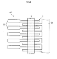
- Figs. 1 and 2 show a thermal printhead according to a first embodiment of the present invention.
- the illustrated thermal printhead A1 includes a substrate 1, an electrode pattern 2, a heating resistor 3, a glass layer 4 and a protective film 5. It is to be noted that only the electrode pattern 2 and the heating resistor 3 are shown in Fig. 2 .
- the substrate 1 comprises an insulating substrate which is rectangular in plan view and elongated in the primary scanning direction.
- the substrate is made of e.g. alumina ceramic material.
- a partial glaze 11 is formed on the upper surface of the substrate 1.
- the partial glaze 11 is in the form of a strip extending in the primary scanning direction. As will be understood from the sectional view of Fig. 1 , the partial glaze 11 bulges in the thickness direction of the substrate 1.
- the electrode pattern 2 is provided for applying current to the heating resistor 3 and includes a common electrode 21 and a plurality of individual electrodes 22.
- the common electrode 21 comprises a strip portion extending in the primary scanning direction and a plurality of comb-tooth portions extending in the secondary scanning direction.
- the ends of the individual electrodes 22 and the comb-tooth portions of the common electrode are alternately arranged in the primary scanning direction.
- the electrode pattern 2 is formed by thick film printing of resinate Au paste and the subsequent baking of the paste.
- the heating resistor 3 is a heat generating source of the thermal printhead A1.
- the heating resistor 3 is in the form of a strip elongated in the primary scanning direction and extends across the comb-tooth portions of the common electrode 21 and ends of the individual electrodes 22.
- the portion is heated.
- the heating resistor 3 is formed by thick film printing of ruthenium oxide paste and the subsequent baking of the paste.
- the glass layer 4 covers the partial glaze 11, the electrode pattern 2 and the heating resistor 3.
- the glass layer 4 is formed by thick film printing of glass paste and the subsequent baking of the paste.
- the glass layer 4 has a thickness of about 6.0 ⁇ m.
- the protective film 5 is formed on the glass layer 4 and covers the heating resistor 3 via the glass layer 4.
- the protective layer 5 comprises a first layer 51 having a relatively high thermal conductivity, a second layer 52 having a relatively low thermal conductivity, and a third layer 53 made of a hard material.
- the first layer 51 is made of e.g. SiC and has a thickness of about 3.0 ⁇ m.
- the thermal conductivity of the second layer 52 is lower than that of the first layer 51.
- the second layer 52 is made of e.g. TaN and has a thickness of about 0.8 ⁇ m.
- the third layer 52 is made of e.g. electrically conductive Sialon and has a thickness of about 0.2 ⁇ m.
- the third layer 53 is made of a very hard material, so that it is not damaged due to contact with thermal paper, although the thickness is relatively small.
- the first layer 51, the second layer 52, the third layer 53 are formed by sputtering.
- thermal printhead A1 The advantages of the thermal printhead A1 will be described below.
- the degree of temperature rise and temperature drop of a recording medium such as thermal paper during the printing operation by the thermal printhead A1 is properly adjusted.
- the overall heat transfer coefficient of the entirety of the protective film 5 is determined by the thermal conductivities and thicknesses of the first layer 51, the second layer 52 and the third layer 53.
- the first layer 51 having a relatively large thickness and the second layer 52 having a low thermal conductivity are the main factors which determine the overall heat transfer coefficient.
- the overall heat transfer coefficient is adjusted as desired. For instance, the overall heat transfer coefficient can be increased by increasing the thickness of the first layer 51.
- the thermal paper tends to adhere to the protective film 5. According to this embodiment, however, by properly setting the thicknesses of the first layer 51 and the second layer 52, sticking is prevented without reducing the printing speed. According to the studies performed by the inventors of the present invention, sticking is more reliably prevented when the second layer 52 is made of TaN.
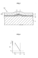
- Fig. 3 shows a thermal printhead A2 according to a second embodiment of the present invention.
- the thermal printhead A2 differs from the thermal printhead A1 in structure of the protective film 5.
- the elements of the second embodiment which are identical or similar to those of the first embodiment are designated by the same reference signs as those used for the first embodiment.
- the protective film 5 of the thermal printhead A2 comprises a single layer made of e.g. SiC.
- the thickness t5 of the protective film 5 is about 4.0 ⁇ m.
- the protective film 5 is so designed that the position in the thickness direction and the thermal conductivity ⁇ has the relationship shown in Fig. 4 .
- the vertical axis of the graph of Fig. 4 indicates the position t in the protective film 5 in the thickness direction (upward direction in Fig. 3 ), and the value t increases as proceeding away from the heating resistor 3.
- the portion which is closest to the heating resistor 3 has a relatively high thermal conductivity ⁇ H (high thermal conductivity portion).
- the portion which is farthest from the heating resistor 3 has a relatively low thermal conductivity ⁇ L ( ⁇ L ⁇ H ) (low thermal conductivity portion).
- the position in the thickness direction and the thermal conductivity ⁇ have a linear relationship.
- such a protective film 5 can be formed by sputtering. In this case, the gas pressure is gradually increased from the start to the end of the film formation process.
- the second embodiment again, the degree of temperature rise and temperature drop of thermal paper is properly adjusted.
- the second embodiment has the same advantages as those of the first embodiment.
- the protective film 5 comprises a single layer, the protective film does not partially peel off.
Landscapes
- Electronic Switches (AREA)
Applications Claiming Priority (2)
| Application Number | Priority Date | Filing Date | Title |
|---|---|---|---|
| JP2006212851A JP4584882B2 (ja) | 2006-08-04 | 2006-08-04 | 厚膜サーマルプリントヘッド |
| PCT/JP2007/064663 WO2008015958A1 (fr) | 2006-08-04 | 2007-07-26 | Tête d'impression thermique |
Publications (1)
| Publication Number | Publication Date |
|---|---|
| EP2052867A1 true EP2052867A1 (fr) | 2009-04-29 |
Family
ID=38997137
Family Applications (1)
| Application Number | Title | Priority Date | Filing Date |
|---|---|---|---|
| EP07791363A Withdrawn EP2052867A1 (fr) | 2006-08-04 | 2007-07-26 | Tête d'impression thermique |
Country Status (5)
| Country | Link |
|---|---|
| US (1) | US7969458B2 (fr) |
| EP (1) | EP2052867A1 (fr) |
| JP (1) | JP4584882B2 (fr) |
| CN (1) | CN101500813B (fr) |
| WO (1) | WO2008015958A1 (fr) |
Families Citing this family (6)
| Publication number | Priority date | Publication date | Assignee | Title |
|---|---|---|---|---|
| JP5392767B2 (ja) * | 2009-10-14 | 2014-01-22 | アオイ電子株式会社 | サーマルヘッド |
| JP5825778B2 (ja) * | 2010-12-10 | 2015-12-02 | ローム株式会社 | サーマルプリントヘッド |
| CN104401135B (zh) * | 2014-12-04 | 2016-11-23 | 山东华菱电子股份有限公司 | 热敏打印头 |
| CN104527231B (zh) * | 2014-12-31 | 2016-10-19 | 山东华菱电子股份有限公司 | 自动去除积碳的热敏打印头及制作方法 |
| CN104512121B (zh) * | 2014-12-31 | 2016-09-14 | 山东华菱电子股份有限公司 | 一种自动去除积碳的热敏打印头及制作方法 |
| CN112297646B (zh) * | 2020-11-17 | 2022-07-05 | 山东华菱电子股份有限公司 | 一种薄膜热敏打印头用发热基板的制造方法 |
Family Cites Families (7)
| Publication number | Priority date | Publication date | Assignee | Title |
|---|---|---|---|---|
| JPS6262775A (ja) * | 1985-09-13 | 1987-03-19 | Seiko Epson Corp | サ−マルヘツド |
| JPH01244870A (ja) * | 1988-03-28 | 1989-09-29 | Nikon Corp | サーマルヘッド |
| US5099257A (en) * | 1989-05-10 | 1992-03-24 | Matsushita Electric Industrial Co., Ltd. | Thermal head with an improved protective layer and a thermal transfer recording system using the same |
| US5157414A (en) * | 1989-09-08 | 1992-10-20 | Hitachi, Ltd. | Thick film type thermal head and thermal recording device |
| US6441840B1 (en) | 2000-06-19 | 2002-08-27 | Rohm Co., Ltd. | Thick-film thermal printhead with improved paper transfer properties |
| JP2002002005A (ja) | 2000-06-19 | 2002-01-08 | Rohm Co Ltd | 厚膜型サーマルプリントヘッド |
| JP4367771B2 (ja) * | 2004-06-15 | 2009-11-18 | ローム株式会社 | サーマルヘッド |
-
2006
- 2006-08-04 JP JP2006212851A patent/JP4584882B2/ja not_active Expired - Fee Related
-
2007
- 2007-07-26 CN CN2007800289734A patent/CN101500813B/zh not_active Expired - Fee Related
- 2007-07-26 WO PCT/JP2007/064663 patent/WO2008015958A1/fr not_active Ceased
- 2007-07-26 US US12/376,384 patent/US7969458B2/en active Active
- 2007-07-26 EP EP07791363A patent/EP2052867A1/fr not_active Withdrawn
Non-Patent Citations (1)
| Title |
|---|
| See references of WO2008015958A1 * |
Also Published As
| Publication number | Publication date |
|---|---|
| WO2008015958A1 (fr) | 2008-02-07 |
| US20100289862A1 (en) | 2010-11-18 |
| JP4584882B2 (ja) | 2010-11-24 |
| JP2008036923A (ja) | 2008-02-21 |
| CN101500813A (zh) | 2009-08-05 |
| US7969458B2 (en) | 2011-06-28 |
| CN101500813B (zh) | 2012-05-16 |
Similar Documents
| Publication | Publication Date | Title |
|---|---|---|
| US7969458B2 (en) | Thermal printhead | |
| US7969459B2 (en) | Thermal print head | |
| JP2008221751A (ja) | サーマルプリントヘッド | |
| US8256099B2 (en) | Manufacturing method for a thermal head | |
| US8031215B2 (en) | Thermal head, thermal printer and manufacturing method of thermal head | |
| CN107020827B (zh) | 热敏打印头及热敏打印机 | |
| US7629990B2 (en) | Thermal print head | |
| US7876343B2 (en) | Thermal print head and method for manufacturing same | |
| JP2008195046A (ja) | サーマルヘッド | |
| KR100395086B1 (ko) | 서멀헤드 및 그 제조방법 | |
| US7843475B2 (en) | Thermal print head and method for manufacturing the same | |
| JP7581000B2 (ja) | サーマルプリントヘッド及びその製造方法、並びにサーマルプリンタ | |
| JP2004155160A (ja) | サーマルヘッド及びその製造方法 | |
| JP5329887B2 (ja) | サーマルヘッド | |
| JP7701181B2 (ja) | サーマルプリントヘッド及びその製造方法、並びにサーマルプリンタ | |
| JP5670076B2 (ja) | サーマルプリントヘッドおよびその製造方法 | |
| JP3481809B2 (ja) | サーマルヘッド | |
| US20070296797A1 (en) | Thermal Print Head and Method for Manufacturing Same | |
| JP2007261118A (ja) | サーマルヘッドおよびその製造方法 | |
| JP4666972B2 (ja) | サーマルヘッド及びそれを用いたサーマルプリンタ | |
| JP2023128840A (ja) | サーマルプリントヘッド | |
| JP5008415B2 (ja) | サーマルヘッド | |
| JP2001010098A (ja) | サーマルヘッド | |
| JP2000135804A (ja) | サーマルヘッド | |
| JPH01229658A (ja) | エッジタイプサーマルヘッド及びその製造方法 |
Legal Events
| Date | Code | Title | Description |
|---|---|---|---|
| PUAI | Public reference made under article 153(3) epc to a published international application that has entered the european phase |
Free format text: ORIGINAL CODE: 0009012 |
|
| 17P | Request for examination filed |
Effective date: 20090225 |
|
| AK | Designated contracting states |
Kind code of ref document: A1 Designated state(s): AT BE BG CH CY CZ DE DK EE ES FI FR GB GR HU IE IS IT LI LT LU LV MC MT NL PL PT RO SE SI SK TR |
|
| AX | Request for extension of the european patent |
Extension state: AL BA HR MK RS |
|
| STAA | Information on the status of an ep patent application or granted ep patent |
Free format text: STATUS: THE APPLICATION HAS BEEN WITHDRAWN |
|
| 18W | Application withdrawn |
Effective date: 20090715 |
|
| RBV | Designated contracting states (corrected) |
Designated state(s): DE FR GB |