EP2053487A2 - Elektrischer Stromkreis und Verfahren zum Entwerfen eines elektrischen Stromkreises - Google Patents
Elektrischer Stromkreis und Verfahren zum Entwerfen eines elektrischen Stromkreises Download PDFInfo
- Publication number
- EP2053487A2 EP2053487A2 EP08166289A EP08166289A EP2053487A2 EP 2053487 A2 EP2053487 A2 EP 2053487A2 EP 08166289 A EP08166289 A EP 08166289A EP 08166289 A EP08166289 A EP 08166289A EP 2053487 A2 EP2053487 A2 EP 2053487A2
- Authority
- EP
- European Patent Office
- Prior art keywords
- clock signal
- clock
- length
- wirings
- circuit
- Prior art date
- Legal status (The legal status is an assumption and is not a legal conclusion. Google has not performed a legal analysis and makes no representation as to the accuracy of the status listed.)
- Withdrawn
Links
Images
Classifications
-
- G—PHYSICS
- G06—COMPUTING OR CALCULATING; COUNTING
- G06F—ELECTRIC DIGITAL DATA PROCESSING
- G06F1/00—Details not covered by groups G06F3/00 - G06F13/00 and G06F21/00
- G06F1/04—Generating or distributing clock signals or signals derived directly therefrom
- G06F1/10—Distribution of clock signals, e.g. skew
-
- G—PHYSICS
- G06—COMPUTING OR CALCULATING; COUNTING
- G06F—ELECTRIC DIGITAL DATA PROCESSING
- G06F30/00—Computer-aided design [CAD]
- G06F30/30—Circuit design
- G06F30/39—Circuit design at the physical level
- G06F30/394—Routing
Definitions
- the present invention relates to an electric circuit associated with transmission of a clock signal and a method for designing the electric circuit.
- electronic equipment including a personal computer or the like uses a memory device of a standard such as Double Data Rate 2 (DDR2) SDRAM, for instance.
- DDR2 Double Data Rate 2
- a plurality or such memory devices may be disposed in electronic equipment for a purpose of securing sufficient memory capacity or other purposes.
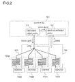
- FIG. 2 A schematic structure of an example of the electric circuit having such the structure is shown in FIG. 2 .
- the electric circuit includes a control IC 101 and a plurality of (e.g., four) SDRAMs 102a to 102d, which are connected to each other via wirings 103 and 104.
- the control IC 101 is provided with a clock signal output portion 111 for outputting a predetermined clock signal and a data input and output portion 112 for supplying or receiving various data to or from the SDRAMs 102a to 102d.
- Such the electric circuit enables the SDRAMs 102a to 102d to read or write data in synchronization with a clock signal (external clock) that is sent from the clock signal output portion 111 via the wiring 103.
- a clock signal external clock
- the clock signal is delivered from the clock signal output portion 111 and is imparted to the SDRAMs 102a to 102d after branching at a branch node 103b.
- the data input and output portion 112 is supplied with the clock signal from the clock signal output portion 111 and performs input and output of data or to the SDRAMs 102a to 102d via the wiring 104 in synchronization with the clock signal.
- the writing operation should be performed in the SDRAMs 102a to 102d at timings delayed as little as possible from the timing when the data to be written reaches the SDRAMs 102a to 102d via the wirings 104.
- a wiring length adjustment portion 103a is disposed at each branch of the individual wirings 103 as shown in FIG. 2 .
- This wiring length adjustment portion 103a is disposed for adjusting the length of the wiring 103 so as to adjust transmission delay time of the clock signal (the longer the wiring, the longer the delay time is).
- a meandering pattern is adopted so that the wiring 103 is adjusted to be longer intentionally and that the transmission delay times of the clock signal to the SDRAMs 102a to 102d are increased.
- the quantity of current of the clock signal is insufficient, it causes drop of an amplitude level of the clock signal or deterioration of a waveform of the clock signal, so that the clock signal cannot be transmitted accurately. Therefore, a malfunction may occur in writing or the like of the data in the SDRAMs 102a to 102d.
- An object of the present invention is to provide an electric circuit and a method for designing the electric circuit that enable to adjust lengths of wirings for transmitting a clock signal to a plurality of processing circuits (e.g., SDRAMs) and still enable to shorten a total length of the wirings.
- a plurality of processing circuits e.g., SDRAMs
- a designing method of an electric circuit includes a clock output circuit for delivering a clock signal and a plurality of processing circuits for receiving the clock signal from the clock output circuit via wirings for clock transmission so as to perform a predetermined process based on the clock signal.
- the method includes, as a method for designing the wirings for clock transmission to have a predetermined length, a first step of connecting wirings between each of the processing circuits and an arbitrary point, as a first point, so that the wiring have substantially the same length, as a first length, and a second step of connecting the first point to the clock output circuit by a single wire having the length that is obtained by subtracting the first length from the predetermined length.
- the length of the wirings for clock transmission can be set to be a predetermined length. Therefore, a delay time in transmission of the clock signal can be adapted to be a predetermined time.
- this setting can be realized by connecting the first point to the clock output circuit by a single wire having the remaining length. As a result, even if a relatively long wiring is required to realize this setting, it is sufficient to increase the length of the single wire. Therefore, it is possible to shorten the entire length of the wirings for transmitting the clock compared with the case where the individual wirings after the branch are required to have increased lengths.
- the predetermined length may be the length such that a delay time of the clock signal due to transmission from the clock output circuit to the processing circuit via the wirings for clock transmission becomes a predetermined time.
- the electric circuit also may include a data output circuit for receiving the clock signal from the clock signal output circuit so as to transmit data to the processing circuit in synchronization with the clock signal
- the processing circuit is a memory circuit for writing the transmitted data in synchronization with the clock signal
- the predetermined time is substantially the same as the time from output of the clock signal by the clock signal output circuit to arrival of the data at the processing circuit.
- the clock signal and the data can be transmitted to the processing circuit (memory circuit) substantially at the same time. Therefore, a process of writing data in the memory circuit can be performed appropriately.
- the wirings for clock transmission may include a branch node disposed between the first point and the processing circuit, and the processing circuit may be disposed at each branch after the branch node.
- wiring lengths after the branch node can be further shortened in the case where the processing circuits are disposed closely or in other cases.
- the single wire may be disposed in a meandering manner, and each of the processing circuits may be a DDR2 SDRAM.
- an electric circuit designed by the above-mentioned designing method and an electrical apparatus equipped with the electric circuit are also useful.
- an electric circuit includes a clock output circuit for delivering a clock signal and a plurality of processing circuits for receiving the clock signal from the clock output circuit via wirings for clock transmission so as to perform a predetermined process based on the clock signal.
- the wirings for clock transmission is connected by a single wire between the clock output circuit and a certain point, as a first point, on the electric circuit, and is further connected between the first point and the individual processing circuits by a plurality of wirings branching from the first point so that the wirings have substantially the same length, and the length of the single wire is adjusted so that a delay time of the clock signal due to transmission from the clock output circuit to the processing circuit via the wirings for clock transmission, becomes a predetermined time.
- a delay time of the clock signal in the processing circuit can be adapted to be a predetermined time.
- the length of the single wire is adjusted, it is possible to shorten the entire length of the wirings (or decrease power loss) compared with the structure in which lengths of individual wirings after the branch node (after the first point) are adjusted, so that it is easy to avoid insufficient quantity of current of the clock signal.
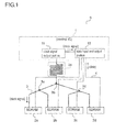
- FIG 1 is a structural diagram of an electric circuit according to an embodiment of the present invention.
- FIG. 2 is a structural diagram according to an example of a conventional electric circuit.
- an electric circuit 9 includes a control IC 1 and four SDRAMs (Synchronous DRAMs) 2a to 2d).
- the control IC includes a clock signal output portion 11 and a data input and output portion 12.
- the clock signal output portion 11 generates a clock signal having a predetermined frequency, which is transmitted to the data input and output portion 12, the individual SDRAMs 2a to 2d, and the like. Note that the transmission of the clock signal to the individual SDRAMs 2a to 2d is performed via the wiring 3 that connects them with each other.
- the data input and output portion 12 performs input and output of various data with respect to the SDRAMs 2a to 2d.
- the input and output of data is performed via the wirings 4 that connect them with each other.
- this input and output operation is performed in synchronization with the clock signal supplied from the clock signal output portion 11.
- the SDRAMs 2a to 2d to be used are ones of Double Data Rate 2 (DDR2) SDRAM standard, for instance, in which various data are read or written in synchronization with an external clock (here, a clock signal transmitted from the clock signal output portion 11).
- DDR2 Double Data Rate 2
- the data is written in the SDRAMs 2a to 2d in synchronization with the clock signal when the data input and output portion 12 delivers data to the SDRAMs 2a to 2d.
- the SDRAMs 2a to 2d can store the data.
- branch node 3b it branches into lines including a line directed to the SDRAMs 2a and 2b and a line directed to the SDRAMs 2c and 2d.
- each of the SDRAMs 2a to 2d is connected to the clock signal output portion 11 in a so-called tree structure (or in a two-branch tournament structure).
- the wiring from the branch node 3b to the SDRAM 2a via the branch node 3c, the wiring from the branch node 3b to the SDRAM 2b via the branch node 3c, the wiring from the branch node 3b to the SDRAM 2c via the branch node 3d, and the wiring from the branch node 3b to the SDRAM 2d via the branch node 3d are designed to have substantially the same length. In other words, wirings from the first branch node 3b to the individual SDRAMs 2a to 2d have substantially the same length. Furthermore, the single wiring from the clock signal output portion 11 to the branch node 3b, i.e., the wiring upstream the branch node 3b has a wiring length adjustment portion 3a.
- This wiring length adjustment portion 3a is a portion whose wiring length is adjusted arbitrarily in a designing stage of the circuit, and it has a meandering pattern as shown in FIG. 1 , for instance. This pattern facilitates to adjust the length of the single line wiring by changing a width and/or intervals of the meandering pattern without changing a position of the clock signal output portion 11 and the branch node 3b.
- the wiring length adjustment portion 3 a is not limited to the form described above but can have various forms. Thus, in the designing stage of the circuit, delay times of the clock signal to be transmitted to the individual SDRAMs 2a to 2d can be adjusted easily via a length of the wiring 3. Note that a delay time of a signal to be transmitted through a wiring is longer as the wiring is longer as understood well.
- This adjustment of the wiring length by the wiring length adjustment portion 3 a enables to set the time necessary for the data corresponding to the clock to reach the SDRAMs 2a to 2d via the wiring 4 after the clock output by the clock signal output portion 11 to be substantially the same as the time for the clock to reach the SDRAMs 2a to 2d via the wiring 3.
- the wiring length in the wiring length adjustment portion 3a is adjusted so that the time necessary for the data to reach the SDRAMs 2a to 2d with respect to the clock output timing by the clock signal output portion 11 becomes the same as the time necessary for the clock signal to reach.
- the electric circuit 9 can perform the process for writing data into the SDRAMs 2a to 2d in synchronization with the clock signal appropriately.
- the individual SDRAMs 2a to 2d and the point to be a first branch node (hereinafter referred to as a "first point") in the electric circuit 9 (corresponding to the branch node 3b) are connected to each other via the wiring.
- the wiring lengths from the first point to the individual SDRAMs 2a to 2d are adapted to be substantially the same.
- the position of the first point can be arbitrary, it is preferable to be a position that enables the wiring length from the first point to the individual SDRAMs 2a to 2d to be as short as possible.
- branch nodes (3c and 3d) as shown in FIG. 1 may be disposed appropriately, so that SDRAMs 2a to 2d can be arranged at the branches, respectively.
- branch nodes (3c and 3d) as shown in FIG. 1 may be disposed appropriately, so that SDRAMs 2a to 2d can be arranged at the branches, respectively.
- the clock signal output portion 11 and the first point are connected to each other by the single wire.
- the length of the single wire is adapted so that a length of the wiring 3 becomes a predetermined target length.
- the wiring length adjustment portion 3a shown in FIG. 1 is disposed in the single wire. More specifically, the time from the clock signal output by the clock signal output portion 11 to the arrival of the data at the SDRAMs 2a to 2d is adapted to be substantially the same as the time necessary for the clock signal to reach in the same manner.
- the target length is grasped in advance by determining the time (T1) from the clock signal output by the clock signal output portion 11 to the arrival of the data at the SDRAMs 2a to 2d and by calculating the wiring length in the case where the transmission delay time of the clock signal becomes the time T1, for instance. In other words, a result of this calculation is regarded as the target length.
- the time T1 becomes a total sum of the delay time of the clock signal in the transmission from the clock signal output portion 11 to the data input and output portion 12, the time necessary for the data input and output portion 12 to deliver data to the SDRAMs 2a to 2d after receiving the clock signal, the delay time of the data in transmission from the data input and output portion 12 to the SDRAMs 2a to 2d, and delay times due to other factors.
- the wiring length of the wiring length adjustment portion 3a is adjusted in advance so that the length of the single wire connecting the clock signal output portion 11 with the first point becomes the length that is obtained by subtracting the length of the wiring connecting the first point with the SDRAMs 2a to 2d from the above-mentioned target length (remaining length).
- the above-mentioned adjustment of the wiring length in the wiring length adjustment portion 3a can also be regarded as adjustment of the delay time of the clock signal due to transmission from the clock signal output portion 11 to the SDRAMs 2a to 2d to be a predetermined time.
- the above-mentioned method of designing the electric circuit enables to realize the electric circuit 9 shown in FIG. 1 .
- wiring extensions for four lines are necessary when the wiring extension is performed by the wiring length adjustment portion 103a in the conventional electric circuit shown in FIG. 2
- the equivalent wiring extension in the electric circuit 9 of this embodiment only requires the wiring extension for one line. Therefore, it can shorten the entire length of the wiring 3 comparing with the conventional electric circuit.
- a space necessary for the wiring can be minimized so that a small circuit can be realized.
- the embodiment of the present invention is not limited to this example but can be modified variously without deviating from the scope of the present invention.
- the SDRAMs are exemplified as devices that receive the clock signal in this embodiment, they can be other devices that perform processes based on the clock signal.
- the electric circuit of this embodiment can be applied widely to an electrical apparatus such as a personal computer.
- the length of the wiring for transmitting the clock can be adopted to be a predetermined length according to the method of designing the electric circuit according to the present invention. Therefore, it is possible to set the delay time in transmission of the clock signal to be a predetermined time. In addition, this setting can be realized by connecting the first point to the clock output circuit by the single wire having the remaining length. As a result, even if a relatively long wiring is required to realize this setting, it is sufficient to increase the length of the single wire. Therefore, it is possible to shorten the entire length of the wirings for transmitting the clock compared with the case where the individual wirings after the branch are required to have increased lengths.
Landscapes
- Engineering & Computer Science (AREA)
- Theoretical Computer Science (AREA)
- Physics & Mathematics (AREA)
- General Engineering & Computer Science (AREA)
- General Physics & Mathematics (AREA)
- Computer Hardware Design (AREA)
- Computer Networks & Wireless Communication (AREA)
- Evolutionary Computation (AREA)
- Geometry (AREA)
- Design And Manufacture Of Integrated Circuits (AREA)
- Semiconductor Integrated Circuits (AREA)
Applications Claiming Priority (1)
| Application Number | Priority Date | Filing Date | Title |
|---|---|---|---|
| JP2007277209A JP2009104503A (ja) | 2007-10-25 | 2007-10-25 | 電気回路および電気回路の設計方法 |
Publications (2)
| Publication Number | Publication Date |
|---|---|
| EP2053487A2 true EP2053487A2 (de) | 2009-04-29 |
| EP2053487A3 EP2053487A3 (de) | 2013-03-27 |
Family
ID=40091334
Family Applications (1)
| Application Number | Title | Priority Date | Filing Date |
|---|---|---|---|
| EP08166289A Withdrawn EP2053487A3 (de) | 2007-10-25 | 2008-10-09 | Elektrischer Stromkreis und Verfahren zum Entwerfen eines elektrischen Stromkreises |
Country Status (4)
| Country | Link |
|---|---|
| US (1) | US8001507B2 (de) |
| EP (1) | EP2053487A3 (de) |
| JP (1) | JP2009104503A (de) |
| CN (1) | CN101419482B (de) |
Families Citing this family (8)
| Publication number | Priority date | Publication date | Assignee | Title |
|---|---|---|---|---|
| CN101808460B (zh) * | 2010-03-25 | 2014-06-11 | 中兴通讯股份有限公司 | 用于pcb的布线方法及pcb |
| JP6028867B2 (ja) * | 2014-07-11 | 2016-11-24 | 富士通株式会社 | 設計プログラム、装置及び方法 |
| KR101589949B1 (ko) * | 2015-07-28 | 2016-01-29 | 주식회사 대성글로벌코리아 | 프로세서 유닛과 메모리 유닛 간의 임피던스 매칭을 위한 배선 구조 및 이를 포함하는 uhd 디스플레이 보드 |
| KR101593375B1 (ko) * | 2015-07-28 | 2016-02-11 | 박웅기 | 에러 발생을 줄이기 위한 uhd 디스플레이 보드의 배치 구조 및 이 배치 구조를 갖는 uhd 디스플레이 보드 |
| US10796728B2 (en) * | 2018-08-17 | 2020-10-06 | Micron Technology, Inc. | Wiring with external terminal |
| KR20220048735A (ko) * | 2020-10-13 | 2022-04-20 | 삼성전자주식회사 | 테스트 시간을 줄이는 메모리 장치의 테스트 방법, 메모리 빌트-인 셀프 테스트(mbist) 회로 및 메모리 장치 |
| CN113220622A (zh) * | 2021-05-27 | 2021-08-06 | 浪潮电子信息产业股份有限公司 | 一种主板及时序控制方法、装置 |
| KR102862505B1 (ko) | 2022-08-19 | 2025-09-23 | 테슬라, 인크. | 클럭 스큐를 개선하기 위한 트랙 플랜 |
Citations (5)
| Publication number | Priority date | Publication date | Assignee | Title |
|---|---|---|---|---|
| JP2000122751A (ja) | 1998-10-16 | 2000-04-28 | Matsushita Electric Ind Co Ltd | クロック分配器及びクロックの分配方法 |
| JP2000148282A (ja) | 1998-11-10 | 2000-05-26 | Hitachi Ltd | 半導体装置及び当該装置を搭載したモジュール |
| JP2000267756A (ja) | 1999-03-18 | 2000-09-29 | Nec Corp | クロック分配回路およびクロック分配方法 |
| JP2004110103A (ja) | 2002-09-13 | 2004-04-08 | Canon Inc | クロックのタイミング制御回路ユニット |
| JP2006054348A (ja) | 2004-08-12 | 2006-02-23 | Fujitsu Ltd | 半導体装置、クロック分配方法及びプログラム |
Family Cites Families (9)
| Publication number | Priority date | Publication date | Assignee | Title |
|---|---|---|---|---|
| JPH0588776A (ja) | 1991-09-26 | 1993-04-09 | Nec Corp | Lsiクロツク分配方式 |
| US5784600A (en) * | 1996-07-01 | 1998-07-21 | Sun Microsystems, Inc. | Method of generating exact-length wires for routing critical signals |
| US6223328B1 (en) * | 1996-12-03 | 2001-04-24 | Fujitsu, Limited | Wire processing method, wire processing equipment, and recording medium for wire processing program used in designing a large scale integrated circuit |
| KR100296452B1 (ko) * | 1997-12-29 | 2001-10-24 | 윤종용 | 데이터 입력 버퍼들을 구비한 동기식 반도체 메모리 장치 |
| US6305001B1 (en) * | 1998-06-18 | 2001-10-16 | Lsi Logic Corporation | Clock distribution network planning and method therefor |
| JP3028949B1 (ja) * | 1998-11-12 | 2000-04-04 | 日本電気アイシーマイコンシステム株式会社 | 半導体記憶装置とその形成方法及びその方法を記録した記録媒体 |
| JP2001177046A (ja) | 1999-12-21 | 2001-06-29 | Hitachi Ltd | 半導体装置およびその製造方法 |
| JP2006179112A (ja) | 2004-12-22 | 2006-07-06 | Seiko Epson Corp | 半導体記憶装置 |
| EP1701279A1 (de) * | 2005-03-11 | 2006-09-13 | STMicroelectronics (Research & Development) Limited | Herstellung eines Taktverteilungsnetzwerkes in einer elektrischen Schaltung |
-
2007
- 2007-10-25 JP JP2007277209A patent/JP2009104503A/ja active Pending
-
2008
- 2008-10-09 EP EP08166289A patent/EP2053487A3/de not_active Withdrawn
- 2008-10-14 US US12/285,775 patent/US8001507B2/en not_active Expired - Fee Related
- 2008-10-23 CN CN2008101713890A patent/CN101419482B/zh not_active Expired - Fee Related
Patent Citations (5)
| Publication number | Priority date | Publication date | Assignee | Title |
|---|---|---|---|---|
| JP2000122751A (ja) | 1998-10-16 | 2000-04-28 | Matsushita Electric Ind Co Ltd | クロック分配器及びクロックの分配方法 |
| JP2000148282A (ja) | 1998-11-10 | 2000-05-26 | Hitachi Ltd | 半導体装置及び当該装置を搭載したモジュール |
| JP2000267756A (ja) | 1999-03-18 | 2000-09-29 | Nec Corp | クロック分配回路およびクロック分配方法 |
| JP2004110103A (ja) | 2002-09-13 | 2004-04-08 | Canon Inc | クロックのタイミング制御回路ユニット |
| JP2006054348A (ja) | 2004-08-12 | 2006-02-23 | Fujitsu Ltd | 半導体装置、クロック分配方法及びプログラム |
Also Published As
| Publication number | Publication date |
|---|---|
| JP2009104503A (ja) | 2009-05-14 |
| US20090108893A1 (en) | 2009-04-30 |
| US8001507B2 (en) | 2011-08-16 |
| EP2053487A3 (de) | 2013-03-27 |
| CN101419482A (zh) | 2009-04-29 |
| CN101419482B (zh) | 2013-01-02 |
Similar Documents
| Publication | Publication Date | Title |
|---|---|---|
| US8001507B2 (en) | Electric circuit and method for adjusting wirelength of clock signal in electric circuit | |
| US11990912B2 (en) | Data transmission using delayed timing signals | |
| US6894933B2 (en) | Buffer amplifier architecture for semiconductor memory circuits | |
| US6724685B2 (en) | Configuration for data transmission in a semiconductor memory system, and relevant data transmission method | |
| US8928383B2 (en) | Integrated delayed clock for high speed isolated SPI communication | |
| US20090086522A1 (en) | Address line wiring structure and printed wiring board having same | |
| US8185760B2 (en) | Memory controller device, control method for memory controller device and data reception device | |
| KR100958902B1 (ko) | 위상 조정 기능의 평가 방법, 정보 처리 장치, 및 컴퓨터판독 가능한 정보 기록 매체 | |
| CN114556119B (zh) | 稳定待测设备处的电压 | |
| US6873533B2 (en) | Unbuffered memory system | |
| US7859309B2 (en) | Clock tree distributing method | |
| US20080250263A1 (en) | Integrated Circuit Input/Output Interface with Empirically Determined Delay Matching | |
| KR102195256B1 (ko) | 전자 장치의 테스트 장치 및 시스템 | |
| JP2008140821A (ja) | 半導体装置および半導体装置の設計方法 | |
| US6810486B2 (en) | Method and apparatus for de-skewing a clock using a first and second phase locked loop and a clock tree | |
| US7380152B2 (en) | Daisy chained multi-device system and operating method | |
| JP2007164599A (ja) | メモリモジュール | |
| US6618816B1 (en) | System for compensating delay of high-speed data by equalizing and determining the total phase-shift of data relative to the phase of clock signal transmitted via separate path | |
| US10504569B2 (en) | System and method for controlling phase alignment of clock signals | |
| US9436210B1 (en) | Control—mechanism for selectively shorting clock grid by electrically connecting and disconnecting clock branches once per clock cycle | |
| US7154809B2 (en) | Method for measuring the delay time of a signal line | |
| US8164348B1 (en) | Method and apparatus for tuning delay | |
| JP2901657B2 (ja) | クロック信号供給装置 | |
| JP2012002509A (ja) | テストボード | |
| US6356100B1 (en) | Ground bounce reduction technique using phased outputs and package de-skewing for synchronous buses |
Legal Events
| Date | Code | Title | Description |
|---|---|---|---|
| PUAI | Public reference made under article 153(3) epc to a published international application that has entered the european phase |
Free format text: ORIGINAL CODE: 0009012 |
|
| AK | Designated contracting states |
Kind code of ref document: A2 Designated state(s): AT BE BG CH CY CZ DE DK EE ES FI FR GB GR HR HU IE IS IT LI LT LU LV MC MT NL NO PL PT RO SE SI SK TR |
|
| AX | Request for extension of the european patent |
Extension state: AL BA MK RS |
|
| PUAL | Search report despatched |
Free format text: ORIGINAL CODE: 0009013 |
|
| AK | Designated contracting states |
Kind code of ref document: A3 Designated state(s): AT BE BG CH CY CZ DE DK EE ES FI FR GB GR HR HU IE IS IT LI LT LU LV MC MT NL NO PL PT RO SE SI SK TR |
|
| AX | Request for extension of the european patent |
Extension state: AL BA MK RS |
|
| RIC1 | Information provided on ipc code assigned before grant |
Ipc: G06F 1/10 20060101AFI20130220BHEP Ipc: G06F 17/50 20060101ALI20130220BHEP Ipc: G11C 7/22 20060101ALI20130220BHEP |
|
| AKY | No designation fees paid | ||
| REG | Reference to a national code |
Ref country code: DE Ref legal event code: R108 |
|
| REG | Reference to a national code |
Ref country code: DE Ref legal event code: R108 Effective date: 20131204 |
|
| STAA | Information on the status of an ep patent application or granted ep patent |
Free format text: STATUS: THE APPLICATION IS DEEMED TO BE WITHDRAWN |
|
| 18D | Application deemed to be withdrawn |
Effective date: 20130928 |