EP2053658A2 - Détecteur d'images - Google Patents
Détecteur d'images Download PDFInfo
- Publication number
- EP2053658A2 EP2053658A2 EP08018512A EP08018512A EP2053658A2 EP 2053658 A2 EP2053658 A2 EP 2053658A2 EP 08018512 A EP08018512 A EP 08018512A EP 08018512 A EP08018512 A EP 08018512A EP 2053658 A2 EP2053658 A2 EP 2053658A2
- Authority
- EP
- European Patent Office
- Prior art keywords
- insulating film
- image detector
- substrate
- active matrix
- bonding member
- Prior art date
- Legal status (The legal status is an assumption and is not a legal conclusion. Google has not performed a legal analysis and makes no representation as to the accuracy of the status listed.)
- Withdrawn
Links
Images


Classifications
-
- H—ELECTRICITY
- H10—SEMICONDUCTOR DEVICES; ELECTRIC SOLID-STATE DEVICES NOT OTHERWISE PROVIDED FOR
- H10F—INORGANIC SEMICONDUCTOR DEVICES SENSITIVE TO INFRARED RADIATION, LIGHT, ELECTROMAGNETIC RADIATION OF SHORTER WAVELENGTH OR CORPUSCULAR RADIATION
- H10F39/00—Integrated devices, or assemblies of multiple devices, comprising at least one element covered by group H10F30/00, e.g. radiation detectors comprising photodiode arrays
- H10F39/10—Integrated devices
- H10F39/12—Image sensors
- H10F39/191—Photoconductor image sensors
- H10F39/195—X-ray, gamma-ray or corpuscular radiation imagers
-
- G—PHYSICS
- G01—MEASURING; TESTING
- G01T—MEASUREMENT OF NUCLEAR OR X-RADIATION
- G01T1/00—Measuring X-radiation, gamma radiation, corpuscular radiation, or cosmic radiation
- G01T1/29—Measurement performed on radiation beams, e.g. position or section of the beam; Measurement of spatial distribution of radiation
- G01T1/2914—Measurement of spatial distribution of radiation
- G01T1/2921—Static instruments for imaging the distribution of radioactivity in one or two dimensions; Radio-isotope cameras
- G01T1/2928—Static instruments for imaging the distribution of radioactivity in one or two dimensions; Radio-isotope cameras using solid state detectors
-
- H—ELECTRICITY
- H10—SEMICONDUCTOR DEVICES; ELECTRIC SOLID-STATE DEVICES NOT OTHERWISE PROVIDED FOR
- H10F—INORGANIC SEMICONDUCTOR DEVICES SENSITIVE TO INFRARED RADIATION, LIGHT, ELECTROMAGNETIC RADIATION OF SHORTER WAVELENGTH OR CORPUSCULAR RADIATION
- H10F39/00—Integrated devices, or assemblies of multiple devices, comprising at least one element covered by group H10F30/00, e.g. radiation detectors comprising photodiode arrays
- H10F39/80—Constructional details of image sensors
- H10F39/804—Containers or encapsulations
Definitions
- the present invention relates to an image detector having an active matrix substrate with multitudes of switching elements disposed thereon.
- the FPD includes an active matrix substrate with multitudes of switching elements disposed thereon and an X-ray sensitive layer stacked thereon, and is capable of directly converting X-ray information to digital data.
- the FPD is advantageous over a conventional imaging plate in that it allows for confirmation of a motion picture, as well as instantaneous confirmation of images.
- Japanese Patent No. 3737343 proposes an image detector like that shown in Figure 17 .
- the image detector proposed in Japanese Patent No. 3737343 includes a TFT array substrate 100 with multitudes of TFT switches disposed two-dimensionally, a semiconductor layer 116 which generates charges according to an electromagnetic wave incident thereon and is stacked on the TFT array substrate 100 such that the charges are read out by the TFT array substrate 100, an upper electrode 117 stacked on the semiconductor layer 116, and a protection substrate 118 stacked over the semiconductor layer 116 and upper electrode 117 so as to cover them, and a resin material 119 is filled in a space between the semiconductor layer 116/upper electrode 117 and protection substrate 118, as illustrated in Figure 17 .
- the protection substrate 118 is bonded to the TFT array substrate 100 only with contact surfaces thereof, which may also lead to the detachment of the protection substrate 118 due to lack of the bonding strength.
- the bonding strength between the resin material and organic insulating material is weak, and a detachment problem will eventually arise at the interface between the resin material and TFT array substrate 100 by linear expansion due to temperature change, which will then lead to creeping discharges or wire breakages.
- an object of the present invention to provide an image detector capable of preventing detachment of the resin material from the active matrix substrate.
- An image detector of the present invention includes: an active matrix substrate having a substrate on which multitudes of switching elements are disposed; a semiconductor layer which generates charges according to an electromagnetic wave representing image information irradiated thereon and is stacked on the active matrix substrate such that the charges are read out by the active matrix substrate; a protection substrate disposed opposite to the active matrix substrate; and an insulating bonding member which bonds the protection substrate to the active matrix substrate, in which the insulating bonding member is bonded to the active matrix substrate through an inorganic insulating film disposed in an area around the periphery of the semiconductor layer.
- the protection substrate may be bonded to the active matrix substrate through an organic insulating film.
- the active matrix substrate may include an organic insulating film having a plurality of openings at a bonding area with the insulating bonding member and the inorganic insulating film may be disposed at the openings of the organic insulating film.
- the openings of the organic insulating film may be formed such that a contact area of the insulating bonding member with the inorganic insulating film through the openings corresponds to 20 to 80% of a contact area of the insulating bonding member with the active matrix substrate.
- the active matrix substrate may include multitude of signal wires, and an organic insulating film may be provided over the signal wires or an adjacent area thereof, and the inorganic insulating film may be provided in an area other than the area where the organic insulating film is provided.
- a contact area of the insulating bonding member with the inorganic insulating film may corresponds to 20 to 80% of a contact area of the insulating bonding member with the active matrix substrate.
- the inorganic insulating film may be a SiNx film.
- the insulating bonding member is bonded to the active matrix substrate through the inorganic insulating film disposed in an area around the periphery of the semiconductor layer, so that the adhesiveness between the insulating bonding member and active matrix substrate may be improved. Therefore, detachment of the insulating bonding member due to linear expansion when a temperature change occurs may be prevented, whereby line breakages arising from creeping discharges and the like may be prevented properly. Further, the improvement of the adhesiveness between the insulating bonding member and active matrix substrate allows the protection substrate, which is bonded to the active matrix substrate through the insulating bonding member, to be adequately bonded to the active matrix substrate.
- the protection substrate and active matrix substrate are temporarily bonded by an adhesive, and where the protection substrate is bonded to the active matrix substrate through an organic insulating film, the influence to the underlayer of the active matrix substrate may be reduced.
- the adhesiveness may be further improved by the irregularity produced by the openings in comparison with a case in which an inorganic insulating film is disposed on the entire contact surface of the insulating bonding member with the active matrix substrate.
- an organic insulating film is provided over the signal wires or an adjacent area thereof of the active matrix substrate, and an inorganic insulating film is provided in an area other than the area where the organic insulating film is provided, voltages impressed on the signal wires by creeping discharges from an upper electrode of the active matrix substrate may be reduced and, at the same time, the adhesiveness between the insulating bonding member and active matrix substrate may be improved.
- Figure 1 illustrates a schematic structure of the radiation image detector.
- the radiation image detector includes a TFT array substrate 10 having a substrate on which multitudes of TFT switches are disposed, a semiconductor layer 6 which generates charges according to an electromagnetic wave representing a radiation image irradiated thereon and is stacked on the TFT array substrate 10 such that the charges are read out by the TFT array substrate 10, an upper electrode 7 stacked on the semiconductor layer 6, an insulating bonding member 25 provided so as to cover a peripheral portion of the semiconductor layer 6 and an upper portion of the upper electrode 7 and to bond a protection substrate 18, to be described later, with the TFT array substrate 10, and the protection substrate 18 stacked on the insulating bonding member 25.
- the semiconductor layer 6 generates charges (electrons-holes) therein when irradiated with an electromagnetic wave such as X-ray. That is, the semiconductor layer 6 has electromagnetic wave conductivity and used for converting radiation image information represented by X-ray to charge information.
- the semiconductor layer 6 is made of, for example, a-Se which is an amorphous body consisting primarily of selenium.
- the referent of "consisting primarily of selenium” means that the selenium has a content rate of not less than 50%.
- the characteristics of the semiconductor layer 6 are liable to be significantly degraded by the environment, so that it requires a certain kind of cover for protection from impurity contamination, moisture, and the like. It also needs to have sufficient voltage resistance since a bias voltage of 1 to 10 kV is applied to the upper electrode 7. Consequently, the protection substrate 18 is provided in the radiation image detector of the present embodiment.
- the protection substrate 18 is made of the same material and has the same board thickness as the substrate of the TFT array substrate 10.
- non-alkali glass with a thickness of 0.7mm is used.
- the insulating bonding member 25 is provided for bonding the protection substrate 18 to the TFT array substrate 10 and preventing creeping discharges between the upper electrode 7 and TFT array substrate 10.
- the insulating bonding member 25 is made of an epoxy group material.
- the TFT array substrate 10 will now be described in detail with reference to Figures 2 and 3 .
- the TFT array substrate 10 includes multitudes of pixels disposed two-dimensionally, each having a TFT switch, but Figure 2 illustrates a plan view of one pixel, and Figure 3 is a cross-section taken along the line 3-3 of Figure 2 .
- the TFT array substrate 10 includes a glass substrate 1, a scanning wire 2, a charge storage capacitor electrode (Cs electrode) 14, a gate insulating film 15, a connection electrode 13, a channel layer 8, a contact layer 9, a data wire 3, an insulating protection film 17, an interlayer insulating film 12, and a charge collection electrode 11.
- Cs electrode charge storage capacitor electrode
- a thin film transistor 4 is formed by the scanning wire 2, gate insulating film 15, data wire 3, connection electrode 13, channel layer 8, contact layer 9, and the like, and a charge storage capacitor (Cs) 5 is formed by the Cs electrode 14, gate insulating film 15, connection electrode 13, and the like.
- the glass substrate 1 is a supporting substrate, which is, for example, non-alkali glass.
- the scanning wires 2 and data wires 3 are electrode wires disposed in a grid pattern, and the thin film transistor 4 (TFT switch) is formed adjacent to each of the intersecting points.
- the TFT switch 4 is a switching element, and the source and drain thereof are connected to the data wire 3 and connection electrode 13 respectively.
- the data wire 3 is the source electrode and the connection electrode 13 is the drain electrode of the TFT switch 4. That is, the data wire 3 includes a straight portion as a signal wire and an extended portion for forming the TFT switch 4, and the connection wire 13 is provided such that the TFT switch 4 is connected to the charge storage capacitor 5.
- the gate insulating film 15 is made of SiNx, SiOx, or the like.
- the gate insulating film 15 is provided so as to cover the scanning wire 2 and Cs electrode 14, and the portion thereof over the scanning wire 2 acts as the gate insulating film of the TFT switch 4, and the portion thereof over the Cs electrode 14 acts as the dielectric layer of the charge storage capacitor 5. That is, the charge storage capacitor 5 is a superimposed area of the Cs electrode 14 formed in the same layer as the scanning wire 2 and the connection electrode 13.
- the material of the gate insulating film 15 is not limited to SiNx, SiOx, but an anodized film of scanning wire 2 and Cs electrode 14 may be used in combination therewith.
- the channel layer (i layer) 8 is the channel section of the TFT switch 4, and a current path between the data wire 3 and connection electrode 13.
- the contact layer (n+ layer) 9 provides a contact between the data wire 3 and connection electrode 13.
- the insulating protection film 17 is formed over the data wire 3 and connection electrode 13, that is, substantially over the entire surface (substantially over the entire area) of the glass substrate 1. This may protects the connection electrode 13 and data wire 3 and provides an electrically insulating separation between them.
- the insulating protection film 17 has a contact hole 16 at a predetermined position, i.e., the position over the portion of the connection electrode 13 facing the Cs electrode 14 across the capacitor 5.
- the charge collection electrode 11 is a transparent conductive amorphous oxide film.
- the charge collection electrode 11 is formed so as to fill the contact hole 16 and stacked over the data wire 3 and connection electrode 13.
- the charge collection electrode 11 is in electrical communication with the semiconductor layer 6 so as to be able to collect charges generated in the semiconductor layer 6.
- the interlayer insulating film 12 is an organic insulating film and provides an electrically insulating separation for the TFT switch 4.
- an acrylic resin may be used as for the material of the organic insulating film.
- the contact hole runs through the interlayer insulating film 12 and the charge collection electrode 11 is connected to the connection electrode 13.
- the interlayer insulating film 12 which is the uppermost layer of the TFT array substrate 10 structured in the manner as described above, is formed of an organic insulating film, as described above.
- Direct stacking of the insulating bonding member 25 on the interlayer insulating film 12 will result in insufficient bonding strength between the interlayer insulating film 12 formed of an organic insulating film and the insulating bonding member 25, so that the insulating bonding member 25 may detach from the TFT array substrate 10 due to difference in the linear expansion coefficient among the TFT array substrate 10, semiconductor layer 6, and insulating bonding member 25 when a temperature change occurs.
- This poses problems of creeping discharges and wire breakages in the scanning wires 2 or data wires 3.
- the protection substrate 18 bonded to the TFT array substrate 10 through the insulating bonding member 25 may possibly detach therefrom.
- the TFT array substrate 10 and insulating bonding member 25 are bonded through an inorganic insulating film 19, as illustrated in Figure 1 .
- the material of the inorganic insulating film 19 for example, SiNx is preferable but SiOx may also be used.
- the results of the evaluation conducted by the inventors of the present invention show that the adhesiveness between the insulating bonding member 25 and inorganic insulating film is greater than that between the insulating bonding member 25 and organic insulating film. The evaluation results are shown in Table 1 below. Accordingly, the structure according to the present embodiment may prevent the insulating bonding member 25 from detaching from the TFT array substrate 10.
- the structure may also prevent the protection substrate 18 bonded to the TFT array substrate 10 through the insulating bonding member 25 from detaching therefrom.
- Figure 4 is a top view illustrating the area where the inorganic insulating film 19 is provided. As illustrated in Figure 4 , in the radiation image detector according to the first embodiment, the inorganic insulating film 19 is provided at the entire bonding area of the insulating bonding member 25 to the TFT array substrate 10 and in a manner to enclose the semiconductor layer 6.
- Figure 5 is a cross-sectional view of the radiation image detector of the second embodiment.
- the radiation image detector according to the second embodiment differs from the radiation image detector according to the first embodiment in the shape of the protection substrate 18.
- the protection substrate 18 of the radiation image detector of the second embodiment has a box shape as illustrated in Figure 5 , and is provided so as to cover the entire sides and upper surfaces of the semiconductor layer 6 and upper electrode 7. Then, the protection substrate 18 and TFT array substrate 10 are bonded through the interlayer insulating film 12.
- an inorganic insulating film 19 is provided at the entire bonding area of the insulating bonding member 25 to the TFT array substrate 10 in order to improve the adhesiveness between the insulating bonding member 25 and TFT array substrate 10.
- the inorganic insulating film 19 is provided so as to enclose the semiconductor layer 6.
- Figure 6 is a top view illustrating the area where the inorganic insulating film 19 is provided.
- the other structure of the radiation image detector of the second embodiment is identical to that of the radiation image detector of the first embodiment.
- a TFT array substrate 10 is formed.
- an interlayer insulating film 12 is formed through patterning by photolithography so as not to be formed in an area surround a pixel region where pixels are disposed.
- an inorganic insulating film 19 is formed in the ring-shaped area where the interlayer insulating film 12 has not been provided.
- a metal pattern 22 is also formed.
- a semiconductor layer 6 is formed by depositing a-Se film on the pixel region of the TFT array substrate 10 by vacuum deposition.
- an upper electrode 7 is formed by depositing Au on the semiconductor layer 6 by vacuum deposition.
- an electrode 23 and a terminal 24 for applying a high voltage to the upper electrode 7 are attached.
- the electrode 23 may be formed of Au deposition film or bonded metal tape.
- a protection substrate 18 is placed on the TFT array substrate 10.
- the protection substrate 18 is placed on the interlayer insulating film 12 and bonded thereto by an adhesive.
- an insulating bonding member 25 is formed by injecting an epoxy resin from a not shown through-hole provided in the protection substrate 18 to fill the space between the TFT array substrate 10 and protection substrate 18.
- the protection substrate 18 has a box shape, but it is not limited to this and, for example, the side portion of the protection substrate 18 may be formed with a rib member and the upper portion with a plate-like member.
- Figure 8 is a cross-sectional view of the radiation image detector according to the third embodiment.
- the radiation image detector according to the third embodiment differs from the radiation image detector according to the second embodiment in that it further includes an underlayer 20 under the semiconductor layer 6. It is often the case that a certain layer is provided under the Se layer for several purposes. One of the purposes is to prevent injection of charges (electrons when positive voltage is applied to the upper electrode, or holes when negative voltage is applied thereto) from the charge collection electrodes. This may reduce noise in the Se layer. Another purpose is to control the film quality of Se film of the upper layer. Generally, the growth of a deposited film is largely influenced by the underlayer, and the characteristics and defects of the deposited film change largely. The results of the evaluation conducted by the inventors of the present invention show that a stable Se layer can be obtained by depositing Se on a Sb 2 S 3 layer rather than directly depositing on a TFT array substrate.
- the underlayer 20 is formed using Sb 2 S 3 , as described above, when the bonding section of the underlayer 20 with the TFT array substrate 10 is the interlayer insulating film 12 of an organic insulating film, the adhesiveness between Sb 2 S 3 and the organic insulating film is low which is likely to cause the detachment problem.
- the results of the evaluation conducted by the inventors of the present invention show that the adhesiveness between Sb 2 S 3 and an inorganic insulating film is greater than that between Sb 2 S 3 and an organic insulating film.
- Table 2 Protection Substrate/Insulating Bonding member (epoxy)/Sb 2 S 3 / TFT Array Adhesiveness Temp Table 2 Protection Substrate/Insulating Bonding member (epoxy)/Sb 2 S 3 / TFT Array Adhesiveness Temp.
- the Sb 2 S 3 lies on the entire area under Se layer, but this area requires an organic insulating film so that the inorganic insulating film can not be used.
- Actual panel evaluation shows that the detachment of the film occurred from a peripheral portion. Consequently, the adhesiveness of the entire panel can be improved by strengthening the adhesiveness in the peripheral portion.
- the inorganic insulating film 19 is formed on the entire surface of the TFT array substrate 10, and the underlayer 20 is bonded to the TFT array substrate 10 through the inorganic insulating film 19, as illustrated in Figure 8 .
- the adhesiveness between the underlayer 20 and TFT array substrate 10 may be improved.
- the inorganic insulating film 19 is provided at the entire bonding area of the insulating bonding member 25 to the TFT array substrate 10 in a manner to enclose the semiconductor layer 6 in order to improve the adhesiveness between the insulating bonding member 25 and TFT array substrate 10, as in the second embodiment.
- Figure 9 is a top view illustrating the contact area of the inorganic insulating film 19 with the insulating bonding member 25.
- the TFT array substrate 10 of the radiation image detector according to the third embodiment is formed by first forming the inorganic insulating film 19 on the entire surface of the TFT array substrate 10 and then the interlayer insulating film 12 is formed on the inorganic insulating film 19 through patterning by photolithography.
- the interlayer insulating film 12 is patterned so as not to be formed in an area surrounding the pixel region, and the insulating bonding member 25 and underlayer 20 are provided in the area where the interlayer insulating film 12 has not been formed.
- the other structure of the radiation image detector of the third embodiment is identical to that of the radiation image detector of the second embodiment.
- Figure 10 is a cross-sectional view of the radiation image detector of the fourth embodiment.
- the inorganic insulating film 19 is formed on the entire surface of the TFT array substrate 10 and then the interlayer insulating film 12 is formed on the inorganic insulating film 19 through patterning, as in the third embodiment, but the patterning method is different from that of the third embodiment.
- Figure 11 illustrates the pattern of the interlayer insulating film 12 of the TFT array substrate 10 of the radiation image detector according to the fourth embodiment.
- the insulating film 12 of the TFT array substrate 10 of the radiation image detector according to the fourth embodiment is patterned such that a plurality of openings 12a is formed around the pixel region of the TFT array substrate 10.
- the areas of the semiconductor layer 6 and upper electrode 7 are denoted by dotted lines.
- Patterning of the interlayer insulating film 12 in the manner as described above allows the insulating bonding member 25 to contact the inorganic insulating film 19 through the openings 12a, thereby the adhesiveness between the insulating bonding member 25 and inorganic insulating film 19 may be improved.
- the portions denoted by grid patterns in Figure 11 are the areas where the insulating bonding member 25 contacts the inorganic insulating film 19.
- the openings 12a of the interlayer insulating film 12 are formed such that the contact area of the insulating bonding member 25 with the inorganic insulating film 19 through the openings 12a corresponds to 20 to 80%, and more preferably 30 to 80% of the contact area of the insulating bonding member 25 with the TFT array substrate 10.
- the interlayer insulating film 12 is as thick as 1 to 3 ⁇ m, if the interlayer insulating film 12 is not provided in the entire area surrounding the pixel region of the TFT array substrate 10, as in the radiation image detector of the third embodiment, a large groove with a step of 1 to 3 ⁇ m will be formed. Where such large groove is formed, the thickness of the resist film in the photolithography process in fabricating the TFT becomes uneven, resulting in poor patterning of ITO film.
- the poor patterning may be remedied by providing a plurality of openings 12a in the interlayer insulating film 12 as in the fourth embodiment, instead of not providing the interlayer insulating film 12 in the entire area surrounding the pixel region of the TFT array substrate 10 as in the third embodiment. Further, provision of a deep uneven pattern on the uppermost surface of the TFT array substrate 10 may further improve the bonding strength.
- an underlayer may be provided in the radiation image detector of the fourth embodiment, as in the radiation image detector of the third embodiment.
- Figure 12 is a top view of the radiation image detector according to the fifth embodiment.
- wires 21, such as the scanning wires 2 and data wires 3, of the radiation image detector are extended from the pixel region to the four sides in the outside, as illustrated in Figure 12 .
- a high voltage in the order of several thousands of volts is applied to the upper electrode 7, and although the high voltage is not directly applied to the area where the semiconductor layer 6 is not provided, but several hundreds of volts is impressed between the area and wires 21 by creeping discharge phenomenon or the like. Consequently, in the radiation image detector according to the fifth embodiment, the interlayer insulating film 12 is patterned such that the voltage impressed on the wiring 21 is reduced.
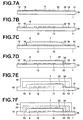
- FIG. 13 a partial cross-sectional view of the radiation image detector according to the fifth embodiment cut out along the wires 21 is shown in Figure 13
- Figure 14 a partial cross-sectional view of the radiation image detector according to the fifth embodiment cut out at a position without the wires 21 is shown in Figure 14 .
- the wires 21 is formed on the glass substrate 1, then the inorganic insulating film 19 is formed thereon, and the interlayer insulating film 12 is formed thereon. Then, as illustrated in Figure 13 , the interlayer insulating film is formed over the wires 21, but it is not formed over the area where the wires 21 are not extended.
- the interlayer insulating film 12 of the TFT array substrate 10 of the radiation image detector according to the fifth embodiment has a pattern like that shown in Figure 15 .
- the interlayer insulating film 12 is formed in the pattern shown in Figure 15 , so that the interlayer insulating film 12 is provided for the area where the wires 21 are extended to reduce the voltage impressed on the wires 21, while the interlayer insulating film 12 is not provided for the area where the wires 21 are not extended to allow the TFT array substrate 10, insulating bonding member 25, and the underlayer 20 to be bonded through the inorganic insulating film 19, so that the adhesiveness of the insulating bonding member 25 and the underlayer 20 to the TFT array substrate 10 may be improved.
- the portion denoted by a grid pattern in Figure 12 is the contact area of the insulating bonding member 25 with the TFT array substrate 10.
- the contact area of the insulating bonding member 25 with the inorganic insulating film 19 corresponds to 20 to 80%, preferably 25 to 65%, and more preferably about 45% of the contact area of the insulating bonding member 25 with the TFT array substrate 10.
- the radiation image detector of the fifth embodiment is a detector in which the wires are extended toward the four sides, as illustrated in Figure 12 .
- the interlayer insulating film may be formed over the wires and not over the area where the wires are not extended.
- the contact area of the insulating bonding member with the inorganic insulating film corresponds to 50 to 80% of the contact area of the insulating bonding member with the TFT array substrate.
- the range may be 25 to 65%, and more preferably about 73%.
- the interlayer insulating film 12 is provided directly above the wires 21 on the TFT array substrate 10, but where the pitch of the wires is small, the interlayer insulating film 12 may be formed in a pattern like that shown in Figure 16 so that the interlayer insulating film 12 is provided over areas adjacent to the wires 21.
- a TFT array substrate having a substrate on which multitudes of TFT switches are disposed is used, but the present invention is also applicable to a radiation image detector with an active matrix substrate having a substrate on which multitudes of switching elements, such as MOS switches, are disposed.
Landscapes
- Physics & Mathematics (AREA)
- Health & Medical Sciences (AREA)
- Life Sciences & Earth Sciences (AREA)
- General Physics & Mathematics (AREA)
- High Energy & Nuclear Physics (AREA)
- Molecular Biology (AREA)
- Spectroscopy & Molecular Physics (AREA)
- Solid State Image Pick-Up Elements (AREA)
- Measurement Of Radiation (AREA)
- Light Receiving Elements (AREA)
Applications Claiming Priority (1)
| Application Number | Priority Date | Filing Date | Title |
|---|---|---|---|
| JP2007275159A JP4940098B2 (ja) | 2007-10-23 | 2007-10-23 | 画像検出器 |
Publications (2)
| Publication Number | Publication Date |
|---|---|
| EP2053658A2 true EP2053658A2 (fr) | 2009-04-29 |
| EP2053658A3 EP2053658A3 (fr) | 2012-05-09 |
Family
ID=40042688
Family Applications (1)
| Application Number | Title | Priority Date | Filing Date |
|---|---|---|---|
| EP08018512A Withdrawn EP2053658A3 (fr) | 2007-10-23 | 2008-10-22 | Détecteur d'images |
Country Status (5)
| Country | Link |
|---|---|
| US (1) | US7968883B2 (fr) |
| EP (1) | EP2053658A3 (fr) |
| JP (1) | JP4940098B2 (fr) |
| CN (1) | CN101419976A (fr) |
| TW (1) | TW200924182A (fr) |
Families Citing this family (3)
| Publication number | Priority date | Publication date | Assignee | Title |
|---|---|---|---|---|
| WO2013080251A1 (fr) * | 2011-11-29 | 2013-06-06 | 株式会社島津製作所 | Détecteur de rayonnement |
| JPWO2013080251A1 (ja) * | 2011-11-29 | 2015-04-27 | 株式会社島津製作所 | 放射線検出器 |
| CN105097852A (zh) * | 2014-05-07 | 2015-11-25 | 中芯国际集成电路制造(上海)有限公司 | 一种半导体器件的制造方法和半导体器件 |
Citations (1)
| Publication number | Priority date | Publication date | Assignee | Title |
|---|---|---|---|---|
| JP3737343B2 (ja) | 1999-09-08 | 2006-01-18 | シャープ株式会社 | 二次元画像検出器 |
Family Cites Families (11)
| Publication number | Priority date | Publication date | Assignee | Title |
|---|---|---|---|---|
| JP3910341B2 (ja) * | 1999-08-04 | 2007-04-25 | シャープ株式会社 | 二次元画像検出器 |
| JP4004761B2 (ja) * | 2001-01-18 | 2007-11-07 | シャープ株式会社 | フラットパネル型イメージセンサ |
| US6891194B2 (en) * | 2001-02-07 | 2005-05-10 | Sharp Kabushiki Kaisha | Active matrix substrate, electromagnetic detector, and liquid crystal display apparatus |
| JP3788740B2 (ja) * | 2001-02-07 | 2006-06-21 | シャープ株式会社 | アクティブマトリクス基板および電磁波検出器 |
| JP3678162B2 (ja) * | 2001-04-12 | 2005-08-03 | 株式会社島津製作所 | 放射線検出装置 |
| JP4066972B2 (ja) * | 2004-03-30 | 2008-03-26 | 株式会社島津製作所 | フラットパネル型放射線検出器 |
| JP2006054232A (ja) * | 2004-08-10 | 2006-02-23 | Toshiba Electron Tubes & Devices Co Ltd | X線検出器およびその製造方法 |
| JP4266898B2 (ja) * | 2004-08-10 | 2009-05-20 | キヤノン株式会社 | 放射線検出装置とその製造方法および放射線撮像システム |
| US7651877B2 (en) * | 2004-10-28 | 2010-01-26 | Sharp Kabushiki Kaisha | Two-dimensional image detecting apparatus and method for manufacturing the same |
| JP2007214236A (ja) * | 2006-02-08 | 2007-08-23 | Toshiba Corp | X線検出器の製造方法およびx線検出器 |
| US7875856B2 (en) * | 2006-02-23 | 2011-01-25 | Shimadzu Corporation | Radiation detector |
-
2007
- 2007-10-23 JP JP2007275159A patent/JP4940098B2/ja not_active Expired - Fee Related
-
2008
- 2008-10-22 TW TW097140381A patent/TW200924182A/zh unknown
- 2008-10-22 US US12/256,047 patent/US7968883B2/en active Active
- 2008-10-22 EP EP08018512A patent/EP2053658A3/fr not_active Withdrawn
- 2008-10-23 CN CNA2008101708977A patent/CN101419976A/zh active Pending
Patent Citations (1)
| Publication number | Priority date | Publication date | Assignee | Title |
|---|---|---|---|---|
| JP3737343B2 (ja) | 1999-09-08 | 2006-01-18 | シャープ株式会社 | 二次元画像検出器 |
Also Published As
| Publication number | Publication date |
|---|---|
| US7968883B2 (en) | 2011-06-28 |
| CN101419976A (zh) | 2009-04-29 |
| JP4940098B2 (ja) | 2012-05-30 |
| EP2053658A3 (fr) | 2012-05-09 |
| TW200924182A (en) | 2009-06-01 |
| US20090101907A1 (en) | 2009-04-23 |
| JP2009105201A (ja) | 2009-05-14 |
Similar Documents
| Publication | Publication Date | Title |
|---|---|---|
| US8039809B2 (en) | Sensor panel and image detecting device | |
| US6649438B2 (en) | Manufacturing method for two-dimensional image detectors and two-dimensional image detectors | |
| EP0555907B1 (fr) | Procédé de fabrication d'un réseau à matrices actives à grande surface | |
| US9520438B2 (en) | Electromagnetic wave detecting element | |
| KR100435295B1 (ko) | 방사선 검출장치 | |
| US8530813B2 (en) | Image detecting device | |
| JP3847494B2 (ja) | 二次元画像検出器の製造方法 | |
| JP5366400B2 (ja) | 連続した膜を使用する集積されたmis光電性デバイス | |
| CN110676270B (zh) | 图像传感器 | |
| US7105829B2 (en) | Radiation detector having radiation sensitive semiconductor | |
| US6806472B2 (en) | Switching device of an X-ray sensor and method for manufacturing the same | |
| JP2001274371A (ja) | 撮像装置構造物 | |
| KR20100017833A (ko) | 방사선 검출기 | |
| EP2023163A2 (fr) | Dispositif de détection d'image | |
| US7164112B2 (en) | Photoelectric conversion device for reducing radiation noise on large screen sensors | |
| US6593577B2 (en) | Electromagnetic wave detecting device | |
| JP3910341B2 (ja) | 二次元画像検出器 | |
| US7968883B2 (en) | Image detector | |
| US7705282B2 (en) | EDS protection for an image detecting device | |
| JP4478215B2 (ja) | 耐腐食性イメージング装置 | |
| JP3788740B2 (ja) | アクティブマトリクス基板および電磁波検出器 | |
| JP4846562B2 (ja) | 二次元画像検出器 | |
| CN121099740A (zh) | 成像元件和图像传感器 | |
| JP2025184766A (ja) | 撮像素子およびイメージセンサ | |
| TW202332027A (zh) | 光感測裝置以及製造光感測裝置的方法 |
Legal Events
| Date | Code | Title | Description |
|---|---|---|---|
| PUAI | Public reference made under article 153(3) epc to a published international application that has entered the european phase |
Free format text: ORIGINAL CODE: 0009012 |
|
| AK | Designated contracting states |
Kind code of ref document: A2 Designated state(s): AT BE BG CH CY CZ DE DK EE ES FI FR GB GR HR HU IE IS IT LI LT LU LV MC MT NL NO PL PT RO SE SI SK TR |
|
| AX | Request for extension of the european patent |
Extension state: AL BA MK RS |
|
| PUAL | Search report despatched |
Free format text: ORIGINAL CODE: 0009013 |
|
| AK | Designated contracting states |
Kind code of ref document: A3 Designated state(s): AT BE BG CH CY CZ DE DK EE ES FI FR GB GR HR HU IE IS IT LI LT LU LV MC MT NL NO PL PT RO SE SI SK TR |
|
| AX | Request for extension of the european patent |
Extension state: AL BA MK RS |
|
| RIC1 | Information provided on ipc code assigned before grant |
Ipc: G01T 1/24 20060101ALI20120405BHEP Ipc: H01L 27/146 20060101AFI20120405BHEP |
|
| AKY | No designation fees paid | ||
| REG | Reference to a national code |
Ref country code: DE Ref legal event code: R108 |
|
| REG | Reference to a national code |
Ref country code: DE Ref legal event code: R108 Effective date: 20130116 |
|
| STAA | Information on the status of an ep patent application or granted ep patent |
Free format text: STATUS: THE APPLICATION IS DEEMED TO BE WITHDRAWN |
|
| 18D | Application deemed to be withdrawn |
Effective date: 20121110 |