EP2053659A2 - Affichage électroluminescent organique - Google Patents
Affichage électroluminescent organique Download PDFInfo
- Publication number
- EP2053659A2 EP2053659A2 EP08253421A EP08253421A EP2053659A2 EP 2053659 A2 EP2053659 A2 EP 2053659A2 EP 08253421 A EP08253421 A EP 08253421A EP 08253421 A EP08253421 A EP 08253421A EP 2053659 A2 EP2053659 A2 EP 2053659A2
- Authority
- EP
- European Patent Office
- Prior art keywords
- light emitting
- organic light
- emitting display
- circuit board
- unit
- Prior art date
- Legal status (The legal status is an assumption and is not a legal conclusion. Google has not performed a legal analysis and makes no representation as to the accuracy of the status listed.)
- Granted
Links
Images


Classifications
-
- H—ELECTRICITY
- H10—SEMICONDUCTOR DEVICES; ELECTRIC SOLID-STATE DEVICES NOT OTHERWISE PROVIDED FOR
- H10K—ORGANIC ELECTRIC SOLID-STATE DEVICES
- H10K59/00—Integrated devices, or assemblies of multiple devices, comprising at least one organic light-emitting element covered by group H10K50/00
- H10K59/10—OLED displays
- H10K59/12—Active-matrix OLED [AMOLED] displays
- H10K59/131—Interconnections, e.g. wiring lines or terminals
-
- H—ELECTRICITY
- H05—ELECTRIC TECHNIQUES NOT OTHERWISE PROVIDED FOR
- H05B—ELECTRIC HEATING; ELECTRIC LIGHT SOURCES NOT OTHERWISE PROVIDED FOR; CIRCUIT ARRANGEMENTS FOR ELECTRIC LIGHT SOURCES, IN GENERAL
- H05B33/00—Electroluminescent light sources
- H05B33/02—Details
- H05B33/06—Electrode terminals
Definitions
- Embodiments relate to organic light emitting displays. More particularly, embodiments relate to organic light emitting displays including electrostatic discharge (ESD) protection such that the organic light emitting display may be protected against ESD.
- ESD electrostatic discharge
- an organic light emitting display has a self-emission characteristic, larger viewing angle, improved contrast, improved response speed, and lower power consumption than liquid crystal displays (LCDs).
- LCDs liquid crystal displays
- Organic light emitting displays do not require a back light, and may be lighter and thinner than LCDs.
- Organic light emitting displays generally include a substrate having a pixel region and a non-pixel region, and a container or an encapsulation substrate.
- the container or the encapsulation substrate may face the substrate so as to encapsulate the substrate, and may be attached to the substrate by a sealant, e.g., epoxy.
- a plurality of organic light emitting diodes coupled between scan lines and data lines, and arranged in a matrix manner, form pixels in the pixel region of the substrate. Portions of scan lines and data lines extending from the scan lines and the data lines of the pixel region, power source supply lines for operating the OLEDs, and a scan driver and a data driver for processing external signals supplied through input pads and supplying the processed signals to the scan lines and the data lines are formed in the non-pixel region.
- a film-shaped flexible printed circuit (not shown) is electrically coupled with the pad of the organic light emitting display having the above structure.
- Signals e.g., power source voltages, scan signals, and data signals, are input from the outside through the FPC.
- the scan driver and the data driver respectively supply the scan signals and the data signals to the scan lines and the data lines.
- the OLEDs of the pixels selected by the scan signals emit light corresponding to the data signals.
- the substrate of the organic light emitting display is formed of glass, a relatively large amount of electrostatic discharge (ESD) is generated during manufacturing and/or operation of the organic light emitting display.
- ESD electrostatic discharge
- the OLEDs and/or driving circuits which operate at high speed and at a low voltage, are subjected to such ESD, the OLEDs and/or the driving circuits can erroneously operate and/or can be damaged due to the electric influence.
- the driving circuits are subjected to the externally generated ESD through internal signal lines, operation of the driving circuits can be instantaneously stopped.
- circuit wiring lines are more likely to be broken or shorted.
- the driving circuits are more severely damaged by such ESD as the driving circuits are highly integrated (minimized).
- Embodiments of the invention are therefore directed to organic light emitting displays, which substantially overcome one or more of the problems due to the limitations and disadvantages of the related art.
- ESD electrostatic discharge
- an organic light emitting display adapted to be connectable to an external circuit board, the organic light emitting display including a substrate, a plurality of organic light emitting diodes (OLEDs) on the substrate, and a plurality of input pads coupled with the plurality of OLEDs through wiring lines, the plurality of input pads being connectable to the external circuit board, wherein at least one of the plurality of input pads includes a lead unit extending from a respective one of the wiring lines, and a contact unit contacting the circuit board, and a resistor coupled between the lead unit and the contact unit of the at least one input pad including the lead unit and the contact unit.
- OLEDs organic light emitting diodes
- the organic light emitting display may include driving circuits coupled between the wiring lines and the OLEDs.
- the organic light emitting display may include thin film transistors (TFT) coupled between the driving circuits and the OLEDs.
- TFT thin film transistors
- the resistor may include polysilicon.
- An insulating layer may be arranged between the at least one input pad and the resistor, and wherein the resistor is coupled with the contact unit and the lead unit through contact holes formed in the insulating layer.
- the circuit board may be a flexible printed circuit (FPC).
- FPC flexible printed circuit
- the contact unit may contact the external circuit board.
- the contact unit and the lead unit may contact the external circuit board.
- the lead unit and the contact unit of the at least one input pad may be spaced apart from each other.
- Each of the plurality of input pads may include a lead unit and a contact unit, the lead unit being spaced apart from the corresponding contact unit.
- the resistor may be directly coupled between and may directly contact the lead unit and the contact unit of the at least one of the plurality of input pads.
- the resistor may include a same material as, and may correspond to a same layer as, source and/or drain regions of the OLEDs.
- an organic light emitting display adapted to be connectable to an external circuit board
- the organic light emitting display including a substrate, a plurality of organic light emitting diodes (OLEDs) on the substrate, and a plurality of input pads coupled with the plurality of OLEDs through wiring lines, the plurality of input pads being connectable to the external circuit board, wherein each of the plurality of input pads includes a lead unit extending from a respective one of the wiring lines, and a contact unit contacting the circuit board, the lead unit being spaced apart from the contact unit.
- OLEDs organic light emitting diodes
- the circuit board may contact the contact unit and the lead unit of the respective input pads.
- a resistor may be coupled between the lead unit and the contact unit of each of the input pads.
- the organic light emitting display may include an insulating layer between the lead unit and the contact unit of each of the input pads.
- the lead units and the contact units may include a same material and correspond to a same layer as source, drain, anode and/or cathode electrodes of the OLEDs.
- the input pads may be arranged along an edge portion of the substrate.
- an organic light emitting display as set out in Claim 1.
- Preferred features of this aspect are set out in Claims 2-12.
- an organic light emitting display as set out in Claim 13. Preferred features of this aspect are set out in Claims 14-18.
- FIG. 1 illustrates a plan view of an organic light emitting display according to an embodiment of the present invention
- FIG. 2 illustrates a cross-sectional view of the organic light emitting diode (OLED) of FIG. 1 ;
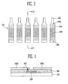
- FIG. 3 illustrates a plan view of exemplary input pads of FIG. 1 ;
- FIG. 4 illustrates a cross-sectional view taken along line I1-I2 of FIG. 3 ;
- FIG. 5 illustrates a plan view of the exemplary input pads of FIGS. 1 and 3 in a state in which a circuit board contacts respective contact units of the input pads;
- FIG. 6 illustrates a cross-sectional view taken along line I11-I12 of FIG. 5 ;
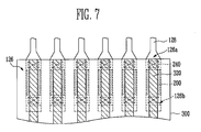
- FIG. 7 illustrates a plan view of the exemplary input pads of FIGS. 1 and 3 in a state in which a circuit board contacts contact units and lead units of the input pads.
- FIG. 1 illustrates a plan view of an organic light emitting display according to an embodiment the invention.
- the organic light emitting display may include a substrate 100, scan lines 122, data lines 124, and organic light emitting diodes (OLEDs) 120, coupled between the scan lines 122 and the data lines 124, in a matrix arrangement.
- OLEDs 120 organic light emitting diodes
- the substrate 100 may include a pixel region 114 and a non-pixel region 116.
- the scan lines 122 and the data lines 124 may extend across the pixel region 114 and the non-pixel region 116.
- respective portions of the scan lines 122 and the data lines 124, power source supply lines (not shown) for operating the OLEDs 120, a scan driver 130, and a data driver 140 may be formed.
- the scan driver 130 and the data driver 140 may process external signals supplied through input pads 126, and may supply the processed signals to the scan lines 122 and the data lines 124, respectively.
- the OLEDs 120 may be coupled between the scan lines 122 and the data lines 124 in a matrix arrangement.
- the OLEDs 120 may be coupled between the scan lines 122 and the data lines 124 in a matrix arrangement together with thin film transistors (TFTs) (not shown) and capacitors (not shown).
- TFTs thin film transistors
- the TFTs may control operations of the OLEDs 120 and the capacitors may function to maintain signals.
- the scan driver 130 and the data driver 140 may be formed on the non-pixel region 116 of the substrate 100.
- the scan driver 120 and the data driver 140 may be manufactured during processing of the OLEDs 120.
- the scan driver 120 and the data driver 140 may be manufactured as an additional integrated circuit semiconductor chip to be attached to the substrate 100, e.g., via a chip on glass (COG) method or a wire bonding method, and electrically coupled with the scan lines 122 and the data lines 124.
- COG chip on glass
- FIG. 2 illustrates a cross-sectional view of the OLED 120 of FIG. 1 , in which an example of the active matrix type OLED is schematically illustrated.
- the OLED may include a buffer layer 101, a semiconductor layer 102, a gate insulating layer 103, a gate electrode 104, an interlayer insulating layer 105, source and drain electrodes 106a and 106b, a planarizing layer 107, an anode electrode 108, a pixel defining layer 109, an organic thin layer 110, and a cathode electrode 111.
- the buffer layer 101 may be formed on the substrate 100.
- the semiconductor layer 102 may be formed on the buffer layer 101.
- the semiconductor layer 102 may provide an active layer. More particularly, the semiconductor layer 102 may provide source, drain, and channel regions of the TFTs.
- the gate insulating layer 103 may be formed on a top surface of the buffer layer 101 and may cover the semiconductor layer 102.
- the gate electrode 104 may be formed on the gate insulating layer 103 formed on the semiconductor layer 102.
- the interlayer insulating layer 105 may be formed on the gate insulating layer 103 and may cover the gate electrode 104.
- Contact holes may be formed in the interlayer insulating layer 105 and the gate insulating layer 103 to expose predetermined parts of the semiconductor layer 102.
- the source and drain electrodes 106a and 106b may be coupled with the semiconductor layer 102 through the contact holes formed on the interlayer insulating layer 105.
- the planarizing layer 107 may be formed on the interlayer insulating layer 105 to cover the source and drain electrodes 106a and 106b.
- a via hole may be formed in the planarizing layer 107 so that the source or drain electrode 106a or 106b may be exposed.
- the anode electrode 108 may be coupled with the source or drain electrode 106a or 106b through the via hole and may be formed on the planarizing layer 107.
- the pixel defining layer 109 may be formed on the planarizing layer 107.
- the pixel defining layer 109 may be patterned to expose the anode electrode 108 in this embodiment.
- the organic thin layer 110 and the cathode electrode 111 may be formed on the anode electrode 108. More particularly, the organic thin layer 110 and the cathode electrode 111 may be formed on the exposed portion of the anode electrode 108.
- the organic thin layer 110 may be formed to have a structure in which a hole transport layer, an organic light emitting layer, and an electron transport layer are laminated together.
- the organic thin layer 110 may further include a hole injection layer and an electron injection layer.
- FIG. 3 illustrates an enlarged plan view of a portion of the organic light emitting display including the input pads 126.
- FIG. 4 illustrates a cross-sectional view taken along line I1-I2 of FIG. 3 .
- FIG. 5 illustrates a plan view of input pads 126 of FIG. 3 in a state in which the external circuit board 300 overlaps and contacts contact portions 126b of the input pads 126, and
- FIG. 6 illustrates a cross-sectional view taken along line 111-I12 of FIG. 5 .
- the input pads 126 may be arranged on the substrate 100 by a predetermined distance.
- the input pads 126 may be coupled with driving circuits of the scan driver 130 and the data driver 140 through wiring lines 128.
- the input pads 126 may be formed at an edge portion of the substrate 100, and may be vulnerable to electrostatic discharge (ESD).
- ESD electrostatic discharge
- resistors 200 for preventing and/or reducing over-current from instantaneously flowing due to the ESD may be included in the input pads 126 and/or the input pads 126 may include a plurality of portions, e.g., lead units 126a and contact units 126b. More particularly, in some embodiments, e.g., the input pads 126 may include lead units 126a that extend from the wiring lines 128 and contact units 126b. The contact units 126b may contact pads of an external circuit board 300 (shown in FIGs. 5 and 7 ). Corresponding pairs of the lead and contact units 126a, 126b may correspond to a respective one of the input pads 126. Further, the lead unit 126a and the corresponding contact unit 126b may be spaced apart from each other, as shown, e.g., in FIGS. 3 and 4 .
- the resistors 200 may be coupled between the lead units 126a and the contact units 126b.
- the resistors 200 may be formed of a conductive material, e.g., polysilicon.
- the resistors 200 may be coupled with the lead units 126a and the contact units 126b through contact holes 240.
- the resistor 200 may be formed on the substrate 100.
- the resistor 200 may be formed of, e.g., polysilicon doped to have a predetermined resistance value.
- An insulating layer 220 may be formed on the substrate 100 where the resistor 200 is formed.
- the lead units 126a and the contact units 126b may be formed to be coupled with respective ends of the resistor 200 through contact holes 240 formed in the insulating layer 220.
- the resistor 200 may be formed of the same material as the semiconductor layer 102, and may be formed during the process of forming the semiconductor layer 102.
- the insulating layer 220 may be formed of the same material as the gate insulating layer 103 and/or the interlayer insulating layer 105.
- the lead units 126a and the contact units 126b may be formed of a same electrode material as and during the process of forming the source and drain electrodes 106a and 106b, the anode electrode 108 and/or the cathode electrode 111.
- the external circuit board 300 does not overlap and/or contact the lead units 126a of the input pads 126.
- embodiments are not limited thereto.
- the circuit board 300 may be coupled with the input pads 126 of the organic light emitting display having the structure illustrated in FIG. 3 .
- the circuit board 300 may be formed of a film-shaped FPC.
- the circuit board 300 may include pads 320.
- the pads 320 of the circuit board 300 may contact the contact units 126b so that signals, e.g., power source voltages, scan signals, and data signals, may be input from the outside.
- the scan driver 130 and the data driver 140 may supply the scan signals and the data signals to the scan lines 122 and the data lines 124, respectively. Therefore, the OLEDs 120 of the pixels selected by the scan signals may emit light corresponding to the data signals. That is, when a predetermined voltage is applied to the anode electrode 108 and the cathode electrode 111 of the OLEDs 120 selected by the scan signals, holes injected through the anode electrode 108 and electrons injected through the cathode electrode 111 may be recombined in the organic thin layer 110 to emit light based on a difference in energy generated by this process. Red, green, or blue light may be emitted from each of the pixels in accordance with materials that form the organic light emitting layer of the respective pixel to realize colors of multi-gray scales.
- the resistors 200 may be formed in the input pads 126, which may be vulnerable to ESD. Over-current caused by ESD may be reduced and/or prevented from flowing by the resistors 200. In some embodiments, all or substantially all of the over-current caused by ESD may be prevented from flowing by the resistors 200. Only driving signals may be supplied to the organic light emitting display so that the driving circuits and the OLEDs may be safely protected.
- the resistors 200 are included in all of the input pads 126. However, embodiments are not limited thereto. For example, in some embodiments, the resistors 200 may be formed only in some of the input pads 126.
- Some embodiments may provide organic light emitting displays that may effectively reduce and/or prevent all and/or substantially all ESD from being received to the input pads 126 through the edge of the substrate 100 in a state where the circuit board 300 is not coupled with the input pads 126.
- Some embodiments may reduce and/or prevent ESD from being received by the substrate 100, from the outside, including from the circuit board 300, through the input pads 126 or from being received by the circuit board 300 from the substrate 100 through the input pads 126 in a state where the circuit board 300 is coupled with the input pads 126.
- FIG. 7 illustrates a plan view of the input pads 126 of FIGS. 1 and 3 in a state in which the circuit board 300 contacts and overlaps respective contact units 126b and lead units 126a of the input pads 126.
- the resistors 200 are included in the embodiment illustrated in FIG. 7 , in embodiments in which the pads 320 of the circuit board overlap and/or contact the lead units 126a and the contact units 126b of the input pads 126, as shown in FIG. 7 , the resistors 200 may be omitted. In such embodiments in which the resistors 200 are omitted, it is possible to prevent wiring line resistance from increasing as a result of the resistors 200.
- resistors may be formed in input pads of an organic light emitting display so that it is possible to prevent and/or reduce over-current caused by ESD received through the substrate or the external circuit board from flowing to the other.
- input pads may include lead units and contact units, and resistors may be coupled between the respective lead units and the contact units so that it is possible to effectively prevent and/or reduce ESD from being received by the organic light emitting display and/or the external circuit board.
- resistors may be formed in input pads of an organic light emitting display so that it is possible to prevent and/or reduce over-current caused by ESD received through the substrate or the external circuit board from flowing to the other.
- input pads may include lead units and contact units, and resistors may be coupled between the respective lead units and the contact units so that it is possible to effectively prevent and/or reduce ESD from being received by the organic light emitting display and/or the external circuit board.
Landscapes
- Engineering & Computer Science (AREA)
- Microelectronics & Electronic Packaging (AREA)
- Electroluminescent Light Sources (AREA)
- Devices For Indicating Variable Information By Combining Individual Elements (AREA)
- Control Of Indicators Other Than Cathode Ray Tubes (AREA)
- Control Of El Displays (AREA)
Applications Claiming Priority (1)
| Application Number | Priority Date | Filing Date | Title |
|---|---|---|---|
| KR1020070106122A KR100911962B1 (ko) | 2007-10-22 | 2007-10-22 | 유기전계발광 표시 장치 |
Publications (3)
| Publication Number | Publication Date |
|---|---|
| EP2053659A2 true EP2053659A2 (fr) | 2009-04-29 |
| EP2053659A3 EP2053659A3 (fr) | 2011-09-28 |
| EP2053659B1 EP2053659B1 (fr) | 2016-04-13 |
Family
ID=40260568
Family Applications (1)
| Application Number | Title | Priority Date | Filing Date |
|---|---|---|---|
| EP08253421.5A Active EP2053659B1 (fr) | 2007-10-22 | 2008-10-22 | Affichage électroluminescent organique |
Country Status (5)
| Country | Link |
|---|---|
| US (1) | US7825585B2 (fr) |
| EP (1) | EP2053659B1 (fr) |
| JP (1) | JP4819025B2 (fr) |
| KR (1) | KR100911962B1 (fr) |
| CN (1) | CN101419978B (fr) |
Families Citing this family (15)
| Publication number | Priority date | Publication date | Assignee | Title |
|---|---|---|---|---|
| US8374960B2 (en) * | 2002-10-29 | 2013-02-12 | Verizon Business Global Llc | Prepaid transaction tracking |
| PL2440015T3 (pl) | 2009-06-05 | 2018-04-30 | Beijing Visionox Technology Co., Ltd. | Organiczne urządzenie elektroluminescencyjne i sposób jego testowania |
| CN101800238B (zh) * | 2009-06-05 | 2013-08-21 | 昆山维信诺显示技术有限公司 | 一种有机电致发光器件 |
| US9412951B2 (en) | 2009-11-13 | 2016-08-09 | Beijing Visionox Technology Co., Ltd. | Organic materials and organic electroluminescent apparatuses using the same |
| KR101082174B1 (ko) | 2009-11-27 | 2011-11-09 | 삼성모바일디스플레이주식회사 | 유기전계발광 표시 장치 및 그의 제조 방법 |
| TWI481300B (zh) * | 2009-12-31 | 2015-04-11 | Univ Tsinghua | Organic electroluminescent devices and their test methods |
| KR101842537B1 (ko) | 2010-11-25 | 2018-03-28 | 삼성디스플레이 주식회사 | 액정 표시 장치 및 액정 표시 장치의 어레이 기판 |
| KR101815255B1 (ko) | 2010-12-16 | 2018-01-08 | 삼성디스플레이 주식회사 | 유기전계발광표시장치 및 이에 적용되는 입력패드 |
| KR101985921B1 (ko) * | 2012-06-13 | 2019-06-05 | 삼성디스플레이 주식회사 | 유기 발광 표시 장치 |
| KR102005483B1 (ko) | 2012-10-19 | 2019-07-31 | 삼성디스플레이 주식회사 | 박막 트랜지스터 기판 및 그의 수리 방법 |
| KR102078386B1 (ko) * | 2013-11-29 | 2020-02-18 | 삼성디스플레이 주식회사 | 유기전계발광 표시장치 |
| KR102230298B1 (ko) | 2014-02-20 | 2021-03-22 | 삼성디스플레이 주식회사 | 표시 장치 및 그 제조 방법 |
| KR102569929B1 (ko) | 2018-07-02 | 2023-08-24 | 삼성디스플레이 주식회사 | 디스플레이 장치 |
| KR102796782B1 (ko) | 2019-10-01 | 2025-04-16 | 삼성디스플레이 주식회사 | 표시 장치 |
| TWI742779B (zh) * | 2020-07-24 | 2021-10-11 | 泰可廣科技股份有限公司 | 具有斜向導線式導電膠條的測試連接器 |
Family Cites Families (22)
| Publication number | Priority date | Publication date | Assignee | Title |
|---|---|---|---|---|
| JPH0254894A (ja) * | 1988-08-17 | 1990-02-23 | Sharp Corp | 薄膜el表示素子 |
| JP2959077B2 (ja) * | 1990-08-18 | 1999-10-06 | セイコーエプソン株式会社 | 半導体装置 |
| US5218222A (en) * | 1992-09-16 | 1993-06-08 | Micron Semiconductor, Inc. | Output ESD protection circuit |
| JP3281174B2 (ja) * | 1994-04-07 | 2002-05-13 | 松下電器産業株式会社 | 液晶表示デバイスおよびその欠陥救済確認の検査方法 |
| JP2874550B2 (ja) * | 1994-04-21 | 1999-03-24 | 日本電気株式会社 | 半導体集積回路装置 |
| JPH0980471A (ja) * | 1995-09-07 | 1997-03-28 | Sony Corp | 液晶表示装置の保護回路 |
| JP3459560B2 (ja) * | 1998-02-10 | 2003-10-20 | 三洋電機株式会社 | 半導体装置及び表示装置 |
| US7301276B2 (en) * | 2000-03-27 | 2007-11-27 | Semiconductor Energy Laboratory Co., Ltd. | Light emitting apparatus and method of manufacturing the same |
| TW484238B (en) * | 2000-03-27 | 2002-04-21 | Semiconductor Energy Lab | Light emitting device and a method of manufacturing the same |
| JP4693262B2 (ja) * | 2000-03-27 | 2011-06-01 | 株式会社半導体エネルギー研究所 | パッシブマトリクス型の発光装置 |
| JP2002214635A (ja) * | 2001-01-18 | 2002-07-31 | Sony Corp | 液晶表示装置 |
| KR20030008345A (ko) | 2001-07-20 | 2003-01-25 | (주)엠큐브게이트 | 인터넷 종합 엔터테인먼트 시스템 및 그 실행 방법 |
| JP3643067B2 (ja) * | 2001-10-11 | 2005-04-27 | 株式会社半導体エネルギー研究所 | 半導体表示装置の設計方法 |
| US6777885B2 (en) * | 2001-10-12 | 2004-08-17 | Semiconductor Energy Laboratory Co., Ltd. | Drive circuit, display device using the drive circuit and electronic apparatus using the display device |
| JP3794368B2 (ja) * | 2002-10-29 | 2006-07-05 | セイコーエプソン株式会社 | El表示装置 |
| JP4519532B2 (ja) * | 2003-06-16 | 2010-08-04 | 株式会社半導体エネルギー研究所 | 発光装置及び発光装置を用いた電子機器 |
| JP4673569B2 (ja) | 2004-03-31 | 2011-04-20 | 株式会社リコー | 半導体装置 |
| JP4026618B2 (ja) * | 2004-05-20 | 2007-12-26 | セイコーエプソン株式会社 | 電気光学装置、その検査方法および電子機器 |
| JP4673579B2 (ja) * | 2004-05-31 | 2011-04-20 | オプトレックス株式会社 | 表示装置 |
| KR100649559B1 (ko) | 2004-06-29 | 2006-11-24 | 삼성에스디아이 주식회사 | Esd 방지 장치 및 이를 구비한 유기 전계 발광 표시 장치 |
| JP2006065284A (ja) * | 2004-07-26 | 2006-03-09 | Seiko Epson Corp | 発光装置及び電子機器 |
| KR100688791B1 (ko) | 2006-01-27 | 2007-03-02 | 삼성에스디아이 주식회사 | 유기 전계 발광 표시장치 및 그 제조 방법. |
-
2007
- 2007-10-22 KR KR1020070106122A patent/KR100911962B1/ko active Active
- 2007-12-07 JP JP2007317512A patent/JP4819025B2/ja active Active
-
2008
- 2008-07-18 US US12/219,261 patent/US7825585B2/en active Active
- 2008-09-05 CN CN200810215316.7A patent/CN101419978B/zh active Active
- 2008-10-22 EP EP08253421.5A patent/EP2053659B1/fr active Active
Non-Patent Citations (1)
| Title |
|---|
| None |
Also Published As
| Publication number | Publication date |
|---|---|
| KR100911962B1 (ko) | 2009-08-13 |
| CN101419978B (zh) | 2014-09-03 |
| JP4819025B2 (ja) | 2011-11-16 |
| JP2009104095A (ja) | 2009-05-14 |
| KR20090040658A (ko) | 2009-04-27 |
| US7825585B2 (en) | 2010-11-02 |
| CN101419978A (zh) | 2009-04-29 |
| EP2053659B1 (fr) | 2016-04-13 |
| EP2053659A3 (fr) | 2011-09-28 |
| US20090102364A1 (en) | 2009-04-23 |
Similar Documents
| Publication | Publication Date | Title |
|---|---|---|
| US7825585B2 (en) | Organic light emitting display | |
| US11895886B2 (en) | Display device with insulating layer in through hole or notch | |
| US7944140B2 (en) | Organic light emitting display and method of manufacturing the same | |
| US11782542B2 (en) | Display device | |
| US9276051B2 (en) | Light-emitting element display device | |
| US8004178B2 (en) | Organic light emitting diode display with a power line in a non-pixel region | |
| KR100839754B1 (ko) | 유기 전계 발광 표시 장치 및 이의 제조 방법 | |
| US10038044B2 (en) | Display device having a driving chip | |
| KR20080023466A (ko) | 평판 표시 장치 | |
| KR101860036B1 (ko) | 씨오지 타입 플렉서블 유기발광소자 | |
| KR20210016114A (ko) | 표시 장치 | |
| KR20170115164A (ko) | 표시 장치 | |
| US11349098B2 (en) | Display device with an improved sealing layer | |
| KR101815255B1 (ko) | 유기전계발광표시장치 및 이에 적용되는 입력패드 | |
| US6876000B2 (en) | Electro-optical device, method of manufacturing the same, and electronic instrument | |
| US7034442B2 (en) | Electro-optical device, method of manufacturing the same, and electronic instrument | |
| US20240065051A1 (en) | Display device | |
| JP2009037124A (ja) | 表示装置及びその製造方法 | |
| KR20200074657A (ko) | 유기발광 표시장치 |
Legal Events
| Date | Code | Title | Description |
|---|---|---|---|
| PUAI | Public reference made under article 153(3) epc to a published international application that has entered the european phase |
Free format text: ORIGINAL CODE: 0009012 |
|
| 17P | Request for examination filed |
Effective date: 20081028 |
|
| AK | Designated contracting states |
Kind code of ref document: A2 Designated state(s): AT BE BG CH CY CZ DE DK EE ES FI FR GB GR HR HU IE IS IT LI LT LU LV MC MT NL NO PL PT RO SE SI SK TR |
|
| AX | Request for extension of the european patent |
Extension state: AL BA MK RS |
|
| PUAL | Search report despatched |
Free format text: ORIGINAL CODE: 0009013 |
|
| RIC1 | Information provided on ipc code assigned before grant |
Ipc: H01L 27/32 20060101AFI20110817BHEP |
|
| AK | Designated contracting states |
Kind code of ref document: A3 Designated state(s): AT BE BG CH CY CZ DE DK EE ES FI FR GB GR HR HU IE IS IT LI LT LU LV MC MT NL NO PL PT RO SE SI SK TR |
|
| AX | Request for extension of the european patent |
Extension state: AL BA MK RS |
|
| AKX | Designation fees paid |
Designated state(s): DE FR GB |
|
| RAP1 | Party data changed (applicant data changed or rights of an application transferred) |
Owner name: SAMSUNG DISPLAY CO., LTD. |
|
| 17Q | First examination report despatched |
Effective date: 20130419 |
|
| RAP1 | Party data changed (applicant data changed or rights of an application transferred) |
Owner name: SAMSUNG DISPLAY CO., LTD. |
|
| GRAP | Despatch of communication of intention to grant a patent |
Free format text: ORIGINAL CODE: EPIDOSNIGR1 |
|
| INTG | Intention to grant announced |
Effective date: 20151008 |
|
| GRAS | Grant fee paid |
Free format text: ORIGINAL CODE: EPIDOSNIGR3 |
|
| GRAA | (expected) grant |
Free format text: ORIGINAL CODE: 0009210 |
|
| AK | Designated contracting states |
Kind code of ref document: B1 Designated state(s): DE FR GB |
|
| REG | Reference to a national code |
Ref country code: GB Ref legal event code: FG4D |
|
| REG | Reference to a national code |
Ref country code: DE Ref legal event code: R096 Ref document number: 602008043466 Country of ref document: DE |
|
| REG | Reference to a national code |
Ref country code: FR Ref legal event code: PLFP Year of fee payment: 9 |
|
| REG | Reference to a national code |
Ref country code: DE Ref legal event code: R097 Ref document number: 602008043466 Country of ref document: DE |
|
| PLBE | No opposition filed within time limit |
Free format text: ORIGINAL CODE: 0009261 |
|
| STAA | Information on the status of an ep patent application or granted ep patent |
Free format text: STATUS: NO OPPOSITION FILED WITHIN TIME LIMIT |
|
| 26N | No opposition filed |
Effective date: 20170116 |
|
| REG | Reference to a national code |
Ref country code: FR Ref legal event code: PLFP Year of fee payment: 10 |
|
| REG | Reference to a national code |
Ref country code: FR Ref legal event code: PLFP Year of fee payment: 11 |
|
| REG | Reference to a national code |
Ref country code: DE Ref legal event code: R079 Ref document number: 602008043466 Country of ref document: DE Free format text: PREVIOUS MAIN CLASS: H01L0027320000 Ipc: H10K0059000000 |
|
| P01 | Opt-out of the competence of the unified patent court (upc) registered |
Effective date: 20230515 |
|
| PGFP | Annual fee paid to national office [announced via postgrant information from national office to epo] |
Ref country code: GB Payment date: 20250922 Year of fee payment: 18 |
|
| PGFP | Annual fee paid to national office [announced via postgrant information from national office to epo] |
Ref country code: FR Payment date: 20250925 Year of fee payment: 18 |
|
| PGFP | Annual fee paid to national office [announced via postgrant information from national office to epo] |
Ref country code: DE Payment date: 20250922 Year of fee payment: 18 |