EP2053697A2 - Connecteur de bus blindé en forme de T - Google Patents
Connecteur de bus blindé en forme de T Download PDFInfo
- Publication number
- EP2053697A2 EP2053697A2 EP08018378A EP08018378A EP2053697A2 EP 2053697 A2 EP2053697 A2 EP 2053697A2 EP 08018378 A EP08018378 A EP 08018378A EP 08018378 A EP08018378 A EP 08018378A EP 2053697 A2 EP2053697 A2 EP 2053697A2
- Authority
- EP
- European Patent Office
- Prior art keywords
- bus
- connection
- bus connector
- connector
- shaped bus
- Prior art date
- Legal status (The legal status is an assumption and is not a legal conclusion. Google has not performed a legal analysis and makes no representation as to the accuracy of the status listed.)
- Granted
Links
Images


Classifications
-
- H—ELECTRICITY
- H01—ELECTRIC ELEMENTS
- H01R—ELECTRICALLY-CONDUCTIVE CONNECTIONS; STRUCTURAL ASSOCIATIONS OF A PLURALITY OF MUTUALLY-INSULATED ELECTRICAL CONNECTING ELEMENTS; COUPLING DEVICES; CURRENT COLLECTORS
- H01R9/00—Structural associations of a plurality of mutually-insulated electrical connecting elements, e.g. terminal strips or terminal blocks; Terminals or binding posts mounted upon a base or in a case; Bases therefor
- H01R9/22—Bases, e.g. strip, block, panel
- H01R9/24—Terminal blocks
- H01R9/26—Clip-on terminal blocks for side-by-side rail- or strip-mounting
- H01R9/2625—Clip-on terminal blocks for side-by-side rail- or strip-mounting with built-in electrical component
- H01R9/2658—Clip-on terminal blocks for side-by-side rail- or strip-mounting with built-in electrical component with built-in data-bus connection
-
- H—ELECTRICITY
- H01—ELECTRIC ELEMENTS
- H01R—ELECTRICALLY-CONDUCTIVE CONNECTIONS; STRUCTURAL ASSOCIATIONS OF A PLURALITY OF MUTUALLY-INSULATED ELECTRICAL CONNECTING ELEMENTS; COUPLING DEVICES; CURRENT COLLECTORS
- H01R13/00—Details of coupling devices of the kinds covered by groups H01R12/70 or H01R24/00 - H01R33/00
- H01R13/648—Protective earth or shield arrangements on coupling devices, e.g. anti-static shielding
- H01R13/658—High frequency shielding arrangements, e.g. against EMI [Electro-Magnetic Interference] or EMP [Electro-Magnetic Pulse]
- H01R13/6598—Shield material
-
- H—ELECTRICITY
- H01—ELECTRIC ELEMENTS
- H01R—ELECTRICALLY-CONDUCTIVE CONNECTIONS; STRUCTURAL ASSOCIATIONS OF A PLURALITY OF MUTUALLY-INSULATED ELECTRICAL CONNECTING ELEMENTS; COUPLING DEVICES; CURRENT COLLECTORS
- H01R9/00—Structural associations of a plurality of mutually-insulated electrical connecting elements, e.g. terminal strips or terminal blocks; Terminals or binding posts mounted upon a base or in a case; Bases therefor
- H01R9/22—Bases, e.g. strip, block, panel
- H01R9/24—Terminal blocks
- H01R9/26—Clip-on terminal blocks for side-by-side rail- or strip-mounting
- H01R9/2675—Electrical interconnections between two blocks, e.g. by means of busbars
-
- H—ELECTRICITY
- H05—ELECTRIC TECHNIQUES NOT OTHERWISE PROVIDED FOR
- H05K—PRINTED CIRCUITS; CASINGS OR CONSTRUCTIONAL DETAILS OF ELECTRIC APPARATUS; MANUFACTURE OF ASSEMBLAGES OF ELECTRICAL COMPONENTS
- H05K7/00—Constructional details common to different types of electric apparatus
- H05K7/14—Mounting supporting structure in casing or on frame or rack
- H05K7/1438—Back panels or connecting means therefor; Terminals; Coding means to avoid wrong insertion
- H05K7/1439—Back panel mother boards
-
- H—ELECTRICITY
- H01—ELECTRIC ELEMENTS
- H01R—ELECTRICALLY-CONDUCTIVE CONNECTIONS; STRUCTURAL ASSOCIATIONS OF A PLURALITY OF MUTUALLY-INSULATED ELECTRICAL CONNECTING ELEMENTS; COUPLING DEVICES; CURRENT COLLECTORS
- H01R31/00—Coupling parts supported only by co-operation with counterpart
- H01R31/02—Intermediate parts for distributing energy to two or more circuits in parallel, e.g. splitter
Definitions
- the invention relates to a T-shaped bus connector which is to be arranged on a carrier device and comprises a holding device for mechanically holding the connector to the carrier device.
- bus connectors or bus socket modules which each connect two adjacent modules together, for example according to DE 198 05 065 A1 .
- a major drawback with this solution is that the packages themselves serve as backplane wiring and that both the bus signals and the power supply are interrupted as soon as an assembly is removed.
- a T-shaped bus connector according to EP 0 896 504 B1 known, which can serve as a bus socket module for one or more modules.
- This bus connector has three connectors, but they are directly connected to each other via metal contacts.
- a disadvantage of the known bus socket modules or bus connectors is, in particular, that future challenges often can not be mastered with these solutions.
- the data signals will become ever faster in the future, and the high-frequency component will thus become ever larger, resulting in a stronger interference emission at the same time.
- the signal levels are getting smaller and the interference from the outside are therefore relatively always greater.
- the line drivers that are suitable for higher data rates are also more sensitive to common mode noise.
- An object of the invention is therefore to be seen to further develop a generic bus connector or a bus socket module such that the electromagnetic compatibility is substantially improved. Further objects of the invention are to be seen in particular in increasing the possible use and flexibility of such bus connectors.
- the invention thus provides a T-shaped bus connector comprising a holding means for mechanically holding the T-shaped bus connector on a support means on which the T-shaped bus connector is to be arranged, and further comprising a first one and a second connection means for respectively establishing an electrical connection to a complementary connection means of a device adjacent to the bus connector, the first and second connection means being in substantially opposite directions and complementary to one another, and one to the first and second Connecting means substantially vertically aligned third connecting means for establishing an electrical connection with a third connecting means complementary connection means of an electrical or electronic assembly, wherein between all three Connecting devices data and / or power bus lines are guided, and all three connection means of the T-shaped bus connector are at least partially surrounded by a shielding material which upon connection of each connection means each having a complementary formed connecting means a complementary connecting means at least partially surrounding shielding material contacted.
- T-shaped bus connectors hereinafter also referred to as bus socket modules
- a backplane bus which advantageously comprises electrical or electronic components via the individual T-shaped bus connectors to the bus system and, moreover, is essentially shielded circumferentially.
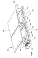
- FIGS. 1 to 5 and 7 to 9 Referring to various embodiments of T-shaped bus connectors according to the invention as well show exemplary arrangements of several, each equipped with an electrical or electronic assembly T-shaped bus connectors.
- a bus socket module or bus connector 100 is provided.
- the electrical or electronic assemblies 200 are merely indicated and may be e.g. connected thereto sensors or actuators include, but will not continue.
- Each bus connector 100 has a holding device for mechanically holding the bus connector to a carrier device 300, to which the bus connector is to be arranged for startup.
- the carrier device 300 is a mounting rail, on which the bus connector according to FIGS. 1 . 4 . 5 and 9 snapped up for commissioning and expediently can be moved to align with adjacent bus connectors on the mounting rail 300.
- two holding arms each having on both sides of the longitudinal axis (reference A1 in Fig. 1 ) of the support rail 300 arranged resilient latching hook 101 is provided which engage around the support rail and allow the displacement of the bus connector 100 and also a simple release of the bus connector 100 on or from the mounting rail.
- two latching hooks or other holding devices which engage around the mounting rail can also be sufficient or provided for securely holding a bus connector according to the invention on a carrier device.
- Fig. 1 are respective holding devices for reasons of clarity not shown.
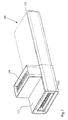
- Each bus connector 100 is designed as a T-shaped bus connector or T-shaped bus socket module.
- the T-shaped structure results from the fact that each bus connector has a first and a second connection means 102 and 103, which face each other in opposite directions when using a support rail 300 expediently each along the longitudinal axis of the support rail looking, and complementary to each other are formed and a first and second connection means substantially vertically aligned third connection means 104 which, in the assembled state of a bus connector in a direction opposite to the carrier device direction.
- the first and second connection devices 102 and 103 respectively serve to establish an electrical connection with a connecting device, which is complementary to the first or second connection device, of a device arranged adjacent to the bus connector and thus make it possible in a simple manner to arrange a multiplicity of T-shaped bus lines. Connectors like the FIGS. 4 . 5 and 9 to see.
- the electrical connection is established with a respective connection device 205 of an electrical or electronic assembly 200 complementary to the third connection device 104.
- all connecting devices 102, 103, 104 and 205 have a substantially rectangular basic shape, with the larger outer surfaces along the transverse axis A2 (FIG. Fig. 1 ) of the mounting rail 300 extend, and the connecting means 102 and 205 have for contacting each a male connector and the complementary thereto each formed connecting means 103 and 104 a complementary to the male connector and mating with this connector.
- connection strips 102, 103 and 104 of a bus connector 100 are preferably held in their position via a printed circuit board 106, which further includes data and power bus lines which are specific to the application between the connection strips 102, 103 and 104 and thus after each Connection preparation of two complementary connection means to these provide the transmission of data and / or energy signals in the desired manner.
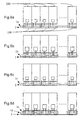
- FIGS. 6a to 6d show various examples of preferred Bus effets between an array of, each equipped with a module 200 T-shaped bus connectors 100 and bus socket modules according to the invention.
- a common supply voltage for all modules or even connected sensors and actuators as well as the associated ground potential can be carried in the bus socket module, as in FIGS Fig. 6a to 6d represented by the marked with the reference numeral 2 wiring.
- the required data signals can vary depending on the application be adapted according to adapted bus line structures, as exemplified in the Fig. 6a to 6d is represented by the cable guides indicated by the reference numerals 1a to 1d.
- a wiring is, according to which the data signals abut as a common bus respectively to all third connection means and thus all modules are connected via this wiring.
- the data signals guided over it are only applied to the third connection devices of groups of three directly juxtaposed bus connectors and the modules connected thereto, so that in each case groups of modules are connected to one another via a common cable routing.
- wiring 1c after Fig. 6c Only the third connection devices of two directly juxtaposed bus connectors are connected to each other in the manner of a point-to-point connection, so that the data signals guided over it each connect two modules in the form of a "daisy chain".
- the combined conductor guide 1c and the two line guides 1d after Fig. 6d In each case, two assemblies in the form of a "daisy chain" are connected to each other again via the line guide 1c and bridged by means of the two line guides 1d each specific assemblies.
- the preferred use of printed circuit boards with application-specific therein or formed thereon data and power bus lines between the first, second and third connection devices 102, 103 and 104 thus allows via the bus socket modules 100 an electrical connection of modules to the bus system, which also allows a module replacement during operation without interrupting the data connection.
- the Data signal connections provided by the lines can in this case be designed as separate transmit and receive connections or as common bidirectional connections.
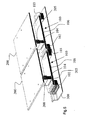
- connection devices 102, 103 and 104 of the T-shaped bus connector 100 are at least partially surrounded by a shielding material in such a way that the shielding material of each of these connection devices, when connected to a respectively complementary connection device, at least partially complements this complementary connection device contacted surrounding shielding material.
- the connecting device 205 of an electronic or electrical assemblies 200 is consequently also surrounded in a preferred embodiment with a shielding material, which contacts the shielding material at least partially surrounding the connecting device 104 when the two connecting devices are brought together.
- the circuit board 106 is expediently at least with regard to the two outer layers 107 (FIG. FIGS. 2, 3 ) also shielded.
- connection devices 102, 103, 104 and 205 illustrated in the figures, according to a first preferred embodiment for forming the shield according to the invention, all three connection devices 102, 103 and 104 of the bus socket module 100 are at least connected to the both larger outer surfaces to be shielded completely with a shroud, in the figures partially identified by 108, and in this case expediently also the connecting device 205 on the respective bus-base module 100 side facing a module 200 also at least on the two larger outer surfaces complete to shield with a shroud, in the figures partially marked 208.
- the shield surfaces 108 and 208 of the connectors are designed so that these with their counterpart in the inserted state along the entire length, ie along the in Fig.
- shield plate 108 and 208 contact springs, such as in Fig. 2 clearly visible and occupied by the reference numeral 109, be arranged, which alternatively, for example, knobs, pressed surfaces o.ä. can be executed.
- These shielding surfaces 108 and 208 are each connected at least once to ground or another suitable potential, for example to a suitable potential of the printed circuit board 106.
- the shorter outer sides or smaller outer surfaces of the connectors 102, 103, 104 and 205 can also be provided with shielding surfaces in this case.
- the outer pins ie, the pins arranged adjacent to the respective shorter outer side of the connector, in the FIGS. 2 and 3 partially denoted by the reference numeral 110, assigned ground or a suitable potential.
- internal pins can also be used for shielding, as long as the data signals are enclosed by ground pins.
- the shield is effected by at least one electrically conductive housing part 111 enclosing the printed circuit board 106.
- the electrically conductive housing part 111 further encloses all three connectors 102, 103 and 104 and has around this connector on the entire length in turn many contact points at a small distance from each other, the conductive housing part 111 of the respective adjacent bus socket module 100 and a the connector 205 on the back of the assembly 200 enclosing shield 211, as in Fig. 9 to see, contact.
- the shield can also be designed, for example, that encloses at least one shield plate, the circuit board of a bus socket module coming from at least one side, in such a shield plate of the screen then by a Outer layer of the circuit board closed becomes.
- the shield plate of a bus socket module in turn around the connector dimensioned and in turn around the connectors on the entire length many contacts at a small distance from each other, that the shield plate of a first bus socket module the respective shield plates of the first bus socket module connected adjacent second bus socket modules and a shroud contacted by the connector on the back of an assembly connected to the first bus socket module.
- the shielding may be e.g. be realized in that the bus socket module is housed in a plastic housing, which is coated with metal so that the metallization is circumferentially a screen, and the connectors again dimensioned and in turn on the whole length many contacts in small Spaced apart from each other, a metallization or shielding sheet is contacted around the backside connector from an assembly coupled to the bus socket module and metallization of an adjacent bus socket module.
- the entire backplane bus constructed from the individual bus socket modules is thus preferably shielded circumferentially according to the invention.
- the shield surrounding at least partially a respective connecting device is dimensioned according to the invention in a particularly expedient manner around the respective connecting device so that around this connecting device the shielding is in each case complementary to the shielding of a complementary connecting device to be coupled with this connecting device.
- the shielding material of the respective shields may also be e.g. be connected to functional ground or with another free potential or with another suitable potential, which is connected directly or via a resistor and / or a capacitor to ground or functional earth.
Landscapes
- Engineering & Computer Science (AREA)
- Microelectronics & Electronic Packaging (AREA)
- Details Of Connecting Devices For Male And Female Coupling (AREA)
- Multi-Conductor Connections (AREA)
Applications Claiming Priority (1)
| Application Number | Priority Date | Filing Date | Title |
|---|---|---|---|
| DE102007050943A DE102007050943A1 (de) | 2007-10-23 | 2007-10-23 | T-förmiger geschirmter Bus-Verbinder |
Publications (3)
| Publication Number | Publication Date |
|---|---|
| EP2053697A2 true EP2053697A2 (fr) | 2009-04-29 |
| EP2053697A3 EP2053697A3 (fr) | 2010-06-30 |
| EP2053697B1 EP2053697B1 (fr) | 2017-05-03 |
Family
ID=40329072
Family Applications (1)
| Application Number | Title | Priority Date | Filing Date |
|---|---|---|---|
| EP08018378.3A Active EP2053697B1 (fr) | 2007-10-23 | 2008-10-21 | Connecteur de bus blindé en forme de T |
Country Status (4)
| Country | Link |
|---|---|
| US (1) | US7704079B2 (fr) |
| EP (1) | EP2053697B1 (fr) |
| DE (1) | DE102007050943A1 (fr) |
| ES (1) | ES2629982T3 (fr) |
Cited By (3)
| Publication number | Priority date | Publication date | Assignee | Title |
|---|---|---|---|---|
| WO2011004253A1 (fr) | 2009-07-09 | 2011-01-13 | Phoenix Contact Inc. | Emetteur es à traitement en boucle bifilaire alimenté à partir de la boucle bifilaire |
| WO2015103469A1 (fr) | 2014-01-03 | 2015-07-09 | Brian Vogt | Réseau de bus de terrain avec une boucle à deux fils |
| EP3993190A1 (fr) * | 2020-11-03 | 2022-05-04 | Bender GmbH & Co. KG | Agencement de bus à rail de support avec adressage automatique de bus |
Families Citing this family (12)
| Publication number | Priority date | Publication date | Assignee | Title |
|---|---|---|---|---|
| DE102009057068A1 (de) * | 2009-12-04 | 2011-06-09 | Wincor Nixdorf International Gmbh | Vorrichtung zur Handhabung von Wertscheinen |
| JP5385864B2 (ja) * | 2010-06-25 | 2014-01-08 | 株式会社日立製作所 | 連結型制御装置 |
| DE102010044201A1 (de) * | 2010-11-21 | 2012-05-24 | Rudi Berthel | Anreih-Modulgehäuse und diese umfassendes Anreih-Modulsystem sowie Montageverfahren |
| DE102012204026B4 (de) | 2012-03-14 | 2016-02-18 | Dinkle Enterprise Co., Ltd. | Datenbusstruktur für Anschlussblöcke, Anschlussblöcke, die diese verwenden, und Anordnung aus einer solchen Datenbusstruktur |
| US9136648B2 (en) * | 2012-07-12 | 2015-09-15 | Rockwell Automation Technologies, Inc. | Din or panel ground integral to connector body |
| DE102012213258A1 (de) * | 2012-07-27 | 2014-01-30 | Siemens Aktiengesellschaft | Verbindungssystem |
| DE102014111030B4 (de) * | 2014-08-04 | 2017-02-09 | Beckhoff Automation Gmbh | Koppeleinheit und industrielles Steuerungssystem |
| TWI692152B (zh) * | 2017-02-07 | 2020-04-21 | 美商莫仕有限公司 | 電連接裝置及板對板電連接組合 |
| TWI697161B (zh) | 2018-03-09 | 2020-06-21 | 町洋企業股份有限公司 | 含有多數功能模組的系統及其功能模組編址方法 |
| BE1026797B1 (de) | 2018-11-26 | 2020-06-22 | Phoenix Contact Gmbh & Co | Modulare Schaltvorrichtung zum Ansteuern wenigstens eines elektrischen Antriebs |
| TWI709307B (zh) * | 2019-04-15 | 2020-11-01 | 町洋企業股份有限公司 | 含有多數功能模組的控制系統及其功能模組編址方法 |
| US12401146B2 (en) * | 2019-12-12 | 2025-08-26 | Fci Usa Llc | Card-edge connector system with busbar connection for high-power applications |
Citations (6)
| Publication number | Priority date | Publication date | Assignee | Title |
|---|---|---|---|---|
| DE19515538A1 (de) | 1995-04-27 | 1996-10-31 | Wacker Chemie Gmbh | Oberflächenbehandelte Metallpulver und deren Verwendung in wäßrigen Beschichtungszusammensetzungen |
| DE3740290C2 (de) | 1987-11-27 | 1997-01-16 | Licentia Gmbh | Vorrichtung zum Steuern und/oder Regeln von Prozessen |
| DE19524123C1 (de) | 1995-05-26 | 1997-02-13 | Phoenix Contact Gmbh & Co | Tragschiene und Stecker zur Kopplung mit einer Tragschiene |
| EP0896504A2 (fr) | 1997-08-05 | 1999-02-10 | PHOENIX CONTACT GmbH & Co. | Appareil électrique ou électronique |
| DE19805065A1 (de) | 1998-02-10 | 1999-08-19 | Vipa Ges Fuer Visualisierung U | Selbstaufbauende Buskontaktiervorrichtung für ein modulares Baugruppensystem |
| EP0527247B1 (fr) | 1991-08-08 | 2000-02-02 | Siemens Aktiengesellschaft | Bus se construisant automatiquement |
Family Cites Families (8)
| Publication number | Priority date | Publication date | Assignee | Title |
|---|---|---|---|---|
| US5387127A (en) * | 1993-08-26 | 1995-02-07 | Wang; Tsan-Chi | Shielding device for T-type BNC connectors |
| DE4345217C2 (de) * | 1993-09-14 | 1995-07-13 | Gaertner Karl Telegaertner | Anschlußkabel zur Bildung einer Anschlußeinrichtung für ein Datennetz |
| DE19610559A1 (de) * | 1996-03-18 | 1997-09-25 | Siemens Ag | Speicherprogrammierbare Steuerung |
| DE19642953A1 (de) * | 1996-10-17 | 1998-04-23 | Bosch Gmbh Robert | Fernmeldevermittlungsanlage |
| DE19838493C1 (de) * | 1998-08-25 | 2000-05-11 | Stahl R Schaltgeraete Gmbh | Anreihbare Busschiene |
| EP1607810B1 (fr) * | 2004-06-07 | 2009-09-30 | Siemens Aktiengesellschaft | Equipement électrique d'entretien facile |
| US7278856B2 (en) * | 2004-08-31 | 2007-10-09 | Fci Americas Technology, Inc. | Contact protector for electrical connectors |
| US6986682B1 (en) * | 2005-05-11 | 2006-01-17 | Myoungsoo Jeon | High speed connector assembly with laterally displaceable head portion |
-
2007
- 2007-10-23 DE DE102007050943A patent/DE102007050943A1/de not_active Ceased
-
2008
- 2008-10-03 US US12/245,137 patent/US7704079B2/en active Active
- 2008-10-21 ES ES08018378.3T patent/ES2629982T3/es active Active
- 2008-10-21 EP EP08018378.3A patent/EP2053697B1/fr active Active
Patent Citations (7)
| Publication number | Priority date | Publication date | Assignee | Title |
|---|---|---|---|---|
| DE3740290C2 (de) | 1987-11-27 | 1997-01-16 | Licentia Gmbh | Vorrichtung zum Steuern und/oder Regeln von Prozessen |
| EP0527247B1 (fr) | 1991-08-08 | 2000-02-02 | Siemens Aktiengesellschaft | Bus se construisant automatiquement |
| DE19515538A1 (de) | 1995-04-27 | 1996-10-31 | Wacker Chemie Gmbh | Oberflächenbehandelte Metallpulver und deren Verwendung in wäßrigen Beschichtungszusammensetzungen |
| DE19524123C1 (de) | 1995-05-26 | 1997-02-13 | Phoenix Contact Gmbh & Co | Tragschiene und Stecker zur Kopplung mit einer Tragschiene |
| EP0896504A2 (fr) | 1997-08-05 | 1999-02-10 | PHOENIX CONTACT GmbH & Co. | Appareil électrique ou électronique |
| EP0896504B1 (fr) | 1997-08-05 | 2003-04-02 | Phoenix Contact GmbH & Co. KG | Appareil électrique ou électronique |
| DE19805065A1 (de) | 1998-02-10 | 1999-08-19 | Vipa Ges Fuer Visualisierung U | Selbstaufbauende Buskontaktiervorrichtung für ein modulares Baugruppensystem |
Cited By (6)
| Publication number | Priority date | Publication date | Assignee | Title |
|---|---|---|---|---|
| WO2011004253A1 (fr) | 2009-07-09 | 2011-01-13 | Phoenix Contact Inc. | Emetteur es à traitement en boucle bifilaire alimenté à partir de la boucle bifilaire |
| US8180948B2 (en) | 2009-07-09 | 2012-05-15 | Phoenix Contact America, Inc. | Two-wire loop process IO transmitter powered from the two-wire loop |
| DE112010002852T5 (de) | 2009-07-09 | 2012-09-06 | Phoenix Contact Gmbh & Co. Kg | E/A-Prozesstransmitter mit zweiadriger Stromschleife, gespeist aus der zweiadrigenStromschleife |
| WO2015103469A1 (fr) | 2014-01-03 | 2015-07-09 | Brian Vogt | Réseau de bus de terrain avec une boucle à deux fils |
| EP3993190A1 (fr) * | 2020-11-03 | 2022-05-04 | Bender GmbH & Co. KG | Agencement de bus à rail de support avec adressage automatique de bus |
| US11818859B2 (en) | 2020-11-03 | 2023-11-14 | Bender Gmbh & Co. Kg | Carrier-rail bus assembly with automatic bus addressing |
Also Published As
| Publication number | Publication date |
|---|---|
| US20090104814A1 (en) | 2009-04-23 |
| EP2053697A3 (fr) | 2010-06-30 |
| ES2629982T3 (es) | 2017-08-17 |
| EP2053697B1 (fr) | 2017-05-03 |
| DE102007050943A1 (de) | 2009-04-30 |
| US7704079B2 (en) | 2010-04-27 |
Similar Documents
| Publication | Publication Date | Title |
|---|---|---|
| EP2053697B1 (fr) | Connecteur de bus blindé en forme de T | |
| DE69131269T2 (de) | Stromkreisaufbau für Instrumententafel eines Kraftfahrzeuges und sein Herstellungsverfahren | |
| EP2692025B1 (fr) | Ensemble de connecteur électrique modulaire | |
| EP2783433B1 (fr) | Connecteur avec blindage | |
| EP3562283A1 (fr) | Arrangement modulaire backplane | |
| DE10338279B4 (de) | Steckverbindervorrichtung | |
| EP1978600B1 (fr) | Agencement de platine | |
| DE102021103224A1 (de) | Mehrpoliger Steckverbinder mit mehreren Außenleitern und Verfahren zum Fertigen desselben | |
| EP3679629B1 (fr) | Élément de contact, unité de raccordement de fiche et contrôleur | |
| DE102004013969B4 (de) | Optischer Verbinder | |
| WO2014111271A1 (fr) | Système de blindage d'une connexion électrique enfichable | |
| DE102013200635A1 (de) | Vorrichtung zur Aufnahme von Elektronikbauteilen | |
| EP3382822B1 (fr) | Dispositif d'accouplement enfichable, procédé et utilisation | |
| EP0700131A1 (fr) | Connexion par enfichage pour câblage de panneau arrière | |
| EP0419694A1 (fr) | Module électronique à connecter à un support | |
| EP0755176B1 (fr) | Dispositif pour l'etablissement d'une connexion électrique ou optique, ou les deux | |
| EP2262062B1 (fr) | Connecteur à fiches | |
| DE102020202209B4 (de) | Anordnung von Elektronikmodulen | |
| EP3649705B1 (fr) | Ensemble de support de contact et procédé de montage de l'ensemble de support de contact | |
| EP0822621B1 (fr) | Dispositif de connexion électrique d'un appareil, en particulier d'une autoradio, dans un véhicule automobile | |
| DE19935994A1 (de) | Steckverbinder | |
| DE102013109247A1 (de) | Montageplatte zur Aufnahme elektrischer Funktionseinheiten in einem Schaltschrank oder Rack | |
| DE102015120530B3 (de) | Modularer Stromverteiler zur Herstellung einer mechanischen und elektrischen Verbindung | |
| DE102023132202A1 (de) | Befestigung von Steuergeräten | |
| DE4033428C2 (de) | Steckverbinder für Kabelanschlüsse |
Legal Events
| Date | Code | Title | Description |
|---|---|---|---|
| PUAI | Public reference made under article 153(3) epc to a published international application that has entered the european phase |
Free format text: ORIGINAL CODE: 0009012 |
|
| AK | Designated contracting states |
Kind code of ref document: A2 Designated state(s): AT BE BG CH CY CZ DE DK EE ES FI FR GB GR HR HU IE IS IT LI LT LU LV MC MT NL NO PL PT RO SE SI SK TR |
|
| AX | Request for extension of the european patent |
Extension state: AL BA MK RS |
|
| PUAL | Search report despatched |
Free format text: ORIGINAL CODE: 0009013 |
|
| AK | Designated contracting states |
Kind code of ref document: A3 Designated state(s): AT BE BG CH CY CZ DE DK EE ES FI FR GB GR HR HU IE IS IT LI LT LU LV MC MT NL NO PL PT RO SE SI SK TR |
|
| AX | Request for extension of the european patent |
Extension state: AL BA MK RS |
|
| RIC1 | Information provided on ipc code assigned before grant |
Ipc: H05K 7/14 20060101ALI20100526BHEP Ipc: H01R 13/658 20060101ALI20100526BHEP Ipc: H01R 9/26 20060101AFI20090212BHEP |
|
| 17P | Request for examination filed |
Effective date: 20101217 |
|
| AKX | Designation fees paid |
Designated state(s): AT BE BG CH CY CZ DE DK EE ES FI FR GB GR HR HU IE IS IT LI LT LU LV MC MT NL NO PL PT RO SE SI SK TR |
|
| 17Q | First examination report despatched |
Effective date: 20130709 |
|
| GRAP | Despatch of communication of intention to grant a patent |
Free format text: ORIGINAL CODE: EPIDOSNIGR1 |
|
| STAA | Information on the status of an ep patent application or granted ep patent |
Free format text: STATUS: GRANT OF PATENT IS INTENDED |
|
| INTG | Intention to grant announced |
Effective date: 20161124 |
|
| GRAS | Grant fee paid |
Free format text: ORIGINAL CODE: EPIDOSNIGR3 |
|
| GRAA | (expected) grant |
Free format text: ORIGINAL CODE: 0009210 |
|
| STAA | Information on the status of an ep patent application or granted ep patent |
Free format text: STATUS: THE PATENT HAS BEEN GRANTED |
|
| AK | Designated contracting states |
Kind code of ref document: B1 Designated state(s): AT BE BG CH CY CZ DE DK EE ES FI FR GB GR HR HU IE IS IT LI LT LU LV MC MT NL NO PL PT RO SE SI SK TR |
|
| REG | Reference to a national code |
Ref country code: GB Ref legal event code: FG4D Free format text: NOT ENGLISH |
|
| REG | Reference to a national code |
Ref country code: AT Ref legal event code: REF Ref document number: 890945 Country of ref document: AT Kind code of ref document: T Effective date: 20170515 Ref country code: CH Ref legal event code: EP |
|
| REG | Reference to a national code |
Ref country code: IE Ref legal event code: FG4D Free format text: LANGUAGE OF EP DOCUMENT: GERMAN |
|
| REG | Reference to a national code |
Ref country code: DE Ref legal event code: R096 Ref document number: 502008015267 Country of ref document: DE |
|
| REG | Reference to a national code |
Ref country code: NL Ref legal event code: FP |
|
| REG | Reference to a national code |
Ref country code: ES Ref legal event code: FG2A Ref document number: 2629982 Country of ref document: ES Kind code of ref document: T3 Effective date: 20170817 |
|
| REG | Reference to a national code |
Ref country code: LT Ref legal event code: MG4D |
|
| PG25 | Lapsed in a contracting state [announced via postgrant information from national office to epo] |
Ref country code: NO Free format text: LAPSE BECAUSE OF FAILURE TO SUBMIT A TRANSLATION OF THE DESCRIPTION OR TO PAY THE FEE WITHIN THE PRESCRIBED TIME-LIMIT Effective date: 20170803 Ref country code: GR Free format text: LAPSE BECAUSE OF FAILURE TO SUBMIT A TRANSLATION OF THE DESCRIPTION OR TO PAY THE FEE WITHIN THE PRESCRIBED TIME-LIMIT Effective date: 20170804 Ref country code: HR Free format text: LAPSE BECAUSE OF FAILURE TO SUBMIT A TRANSLATION OF THE DESCRIPTION OR TO PAY THE FEE WITHIN THE PRESCRIBED TIME-LIMIT Effective date: 20170503 Ref country code: LT Free format text: LAPSE BECAUSE OF FAILURE TO SUBMIT A TRANSLATION OF THE DESCRIPTION OR TO PAY THE FEE WITHIN THE PRESCRIBED TIME-LIMIT Effective date: 20170503 Ref country code: FI Free format text: LAPSE BECAUSE OF FAILURE TO SUBMIT A TRANSLATION OF THE DESCRIPTION OR TO PAY THE FEE WITHIN THE PRESCRIBED TIME-LIMIT Effective date: 20170503 |
|
| REG | Reference to a national code |
Ref country code: FR Ref legal event code: PLFP Year of fee payment: 10 |
|
| PG25 | Lapsed in a contracting state [announced via postgrant information from national office to epo] |
Ref country code: IS Free format text: LAPSE BECAUSE OF FAILURE TO SUBMIT A TRANSLATION OF THE DESCRIPTION OR TO PAY THE FEE WITHIN THE PRESCRIBED TIME-LIMIT Effective date: 20170903 Ref country code: BG Free format text: LAPSE BECAUSE OF FAILURE TO SUBMIT A TRANSLATION OF THE DESCRIPTION OR TO PAY THE FEE WITHIN THE PRESCRIBED TIME-LIMIT Effective date: 20170803 Ref country code: PL Free format text: LAPSE BECAUSE OF FAILURE TO SUBMIT A TRANSLATION OF THE DESCRIPTION OR TO PAY THE FEE WITHIN THE PRESCRIBED TIME-LIMIT Effective date: 20170503 Ref country code: SE Free format text: LAPSE BECAUSE OF FAILURE TO SUBMIT A TRANSLATION OF THE DESCRIPTION OR TO PAY THE FEE WITHIN THE PRESCRIBED TIME-LIMIT Effective date: 20170503 Ref country code: LV Free format text: LAPSE BECAUSE OF FAILURE TO SUBMIT A TRANSLATION OF THE DESCRIPTION OR TO PAY THE FEE WITHIN THE PRESCRIBED TIME-LIMIT Effective date: 20170503 |
|
| PG25 | Lapsed in a contracting state [announced via postgrant information from national office to epo] |
Ref country code: CZ Free format text: LAPSE BECAUSE OF FAILURE TO SUBMIT A TRANSLATION OF THE DESCRIPTION OR TO PAY THE FEE WITHIN THE PRESCRIBED TIME-LIMIT Effective date: 20170503 Ref country code: DK Free format text: LAPSE BECAUSE OF FAILURE TO SUBMIT A TRANSLATION OF THE DESCRIPTION OR TO PAY THE FEE WITHIN THE PRESCRIBED TIME-LIMIT Effective date: 20170503 Ref country code: RO Free format text: LAPSE BECAUSE OF FAILURE TO SUBMIT A TRANSLATION OF THE DESCRIPTION OR TO PAY THE FEE WITHIN THE PRESCRIBED TIME-LIMIT Effective date: 20170503 Ref country code: SK Free format text: LAPSE BECAUSE OF FAILURE TO SUBMIT A TRANSLATION OF THE DESCRIPTION OR TO PAY THE FEE WITHIN THE PRESCRIBED TIME-LIMIT Effective date: 20170503 Ref country code: EE Free format text: LAPSE BECAUSE OF FAILURE TO SUBMIT A TRANSLATION OF THE DESCRIPTION OR TO PAY THE FEE WITHIN THE PRESCRIBED TIME-LIMIT Effective date: 20170503 |
|
| REG | Reference to a national code |
Ref country code: DE Ref legal event code: R097 Ref document number: 502008015267 Country of ref document: DE |
|
| PLBE | No opposition filed within time limit |
Free format text: ORIGINAL CODE: 0009261 |
|
| STAA | Information on the status of an ep patent application or granted ep patent |
Free format text: STATUS: NO OPPOSITION FILED WITHIN TIME LIMIT |
|
| 26N | No opposition filed |
Effective date: 20180206 |
|
| PG25 | Lapsed in a contracting state [announced via postgrant information from national office to epo] |
Ref country code: MC Free format text: LAPSE BECAUSE OF FAILURE TO SUBMIT A TRANSLATION OF THE DESCRIPTION OR TO PAY THE FEE WITHIN THE PRESCRIBED TIME-LIMIT Effective date: 20170503 Ref country code: SI Free format text: LAPSE BECAUSE OF FAILURE TO SUBMIT A TRANSLATION OF THE DESCRIPTION OR TO PAY THE FEE WITHIN THE PRESCRIBED TIME-LIMIT Effective date: 20170503 |
|
| REG | Reference to a national code |
Ref country code: CH Ref legal event code: PL |
|
| REG | Reference to a national code |
Ref country code: NL Ref legal event code: MM Effective date: 20171101 |
|
| GBPC | Gb: european patent ceased through non-payment of renewal fee |
Effective date: 20171021 |
|
| REG | Reference to a national code |
Ref country code: IE Ref legal event code: MM4A |
|
| PG25 | Lapsed in a contracting state [announced via postgrant information from national office to epo] |
Ref country code: LI Free format text: LAPSE BECAUSE OF NON-PAYMENT OF DUE FEES Effective date: 20171031 Ref country code: NL Free format text: LAPSE BECAUSE OF NON-PAYMENT OF DUE FEES Effective date: 20171101 Ref country code: CH Free format text: LAPSE BECAUSE OF NON-PAYMENT OF DUE FEES Effective date: 20171031 Ref country code: GB Free format text: LAPSE BECAUSE OF NON-PAYMENT OF DUE FEES Effective date: 20171021 Ref country code: LU Free format text: LAPSE BECAUSE OF NON-PAYMENT OF DUE FEES Effective date: 20171021 |
|
| REG | Reference to a national code |
Ref country code: BE Ref legal event code: MM Effective date: 20171031 |
|
| PG25 | Lapsed in a contracting state [announced via postgrant information from national office to epo] |
Ref country code: BE Free format text: LAPSE BECAUSE OF NON-PAYMENT OF DUE FEES Effective date: 20171031 |
|
| PG25 | Lapsed in a contracting state [announced via postgrant information from national office to epo] |
Ref country code: MT Free format text: LAPSE BECAUSE OF FAILURE TO SUBMIT A TRANSLATION OF THE DESCRIPTION OR TO PAY THE FEE WITHIN THE PRESCRIBED TIME-LIMIT Effective date: 20170503 |
|
| REG | Reference to a national code |
Ref country code: FR Ref legal event code: PLFP Year of fee payment: 11 |
|
| PG25 | Lapsed in a contracting state [announced via postgrant information from national office to epo] |
Ref country code: IE Free format text: LAPSE BECAUSE OF NON-PAYMENT OF DUE FEES Effective date: 20171021 |
|
| PG25 | Lapsed in a contracting state [announced via postgrant information from national office to epo] |
Ref country code: HU Free format text: LAPSE BECAUSE OF FAILURE TO SUBMIT A TRANSLATION OF THE DESCRIPTION OR TO PAY THE FEE WITHIN THE PRESCRIBED TIME-LIMIT; INVALID AB INITIO Effective date: 20081021 |
|
| PG25 | Lapsed in a contracting state [announced via postgrant information from national office to epo] |
Ref country code: CY Free format text: LAPSE BECAUSE OF NON-PAYMENT OF DUE FEES Effective date: 20170503 |
|
| PG25 | Lapsed in a contracting state [announced via postgrant information from national office to epo] |
Ref country code: TR Free format text: LAPSE BECAUSE OF FAILURE TO SUBMIT A TRANSLATION OF THE DESCRIPTION OR TO PAY THE FEE WITHIN THE PRESCRIBED TIME-LIMIT Effective date: 20170503 |
|
| PG25 | Lapsed in a contracting state [announced via postgrant information from national office to epo] |
Ref country code: PT Free format text: LAPSE BECAUSE OF FAILURE TO SUBMIT A TRANSLATION OF THE DESCRIPTION OR TO PAY THE FEE WITHIN THE PRESCRIBED TIME-LIMIT Effective date: 20170503 |
|
| P01 | Opt-out of the competence of the unified patent court (upc) registered |
Effective date: 20230424 |
|
| PGFP | Annual fee paid to national office [announced via postgrant information from national office to epo] |
Ref country code: AT Payment date: 20251020 Year of fee payment: 18 |
|
| PGFP | Annual fee paid to national office [announced via postgrant information from national office to epo] |
Ref country code: IT Payment date: 20251022 Year of fee payment: 18 |
|
| PGFP | Annual fee paid to national office [announced via postgrant information from national office to epo] |
Ref country code: FR Payment date: 20251027 Year of fee payment: 18 |
|
| PGFP | Annual fee paid to national office [announced via postgrant information from national office to epo] |
Ref country code: ES Payment date: 20251118 Year of fee payment: 18 |
|
| PGFP | Annual fee paid to national office [announced via postgrant information from national office to epo] |
Ref country code: DE Payment date: 20251229 Year of fee payment: 18 |