EP2055672A1 - N-halbleiter-kohlenstoffnanomaterial, verfahren zur herstellung von n-halbleiter-kohlenstoffnanomaterial und verfahren zur herstellung einer halbleitervorrichtung - Google Patents
N-halbleiter-kohlenstoffnanomaterial, verfahren zur herstellung von n-halbleiter-kohlenstoffnanomaterial und verfahren zur herstellung einer halbleitervorrichtung Download PDFInfo
- Publication number
- EP2055672A1 EP2055672A1 EP07792744A EP07792744A EP2055672A1 EP 2055672 A1 EP2055672 A1 EP 2055672A1 EP 07792744 A EP07792744 A EP 07792744A EP 07792744 A EP07792744 A EP 07792744A EP 2055672 A1 EP2055672 A1 EP 2055672A1
- Authority
- EP
- European Patent Office
- Prior art keywords
- carbon nanomaterial
- type semiconductor
- functional group
- carbon
- group
- Prior art date
- Legal status (The legal status is an assumption and is not a legal conclusion. Google has not performed a legal analysis and makes no representation as to the accuracy of the status listed.)
- Withdrawn
Links
Images







Classifications
-
- B—PERFORMING OPERATIONS; TRANSPORTING
- B82—NANOTECHNOLOGY
- B82Y—SPECIFIC USES OR APPLICATIONS OF NANOSTRUCTURES; MEASUREMENT OR ANALYSIS OF NANOSTRUCTURES; MANUFACTURE OR TREATMENT OF NANOSTRUCTURES
- B82Y30/00—Nanotechnology for materials or surface science, e.g. nanocomposites
-
- C—CHEMISTRY; METALLURGY
- C01—INORGANIC CHEMISTRY
- C01B—NON-METALLIC ELEMENTS; COMPOUNDS THEREOF; METALLOIDS OR COMPOUNDS THEREOF NOT COVERED BY SUBCLASS C01C
- C01B32/00—Carbon; Compounds thereof
- C01B32/15—Nano-sized carbon materials
- C01B32/158—Carbon nanotubes
- C01B32/168—After-treatment
- C01B32/174—Derivatisation; Solubilisation; Dispersion in solvents
-
- B—PERFORMING OPERATIONS; TRANSPORTING
- B82—NANOTECHNOLOGY
- B82Y—SPECIFIC USES OR APPLICATIONS OF NANOSTRUCTURES; MEASUREMENT OR ANALYSIS OF NANOSTRUCTURES; MANUFACTURE OR TREATMENT OF NANOSTRUCTURES
- B82Y10/00—Nanotechnology for information processing, storage or transmission, e.g. quantum computing or single electron logic
-
- B—PERFORMING OPERATIONS; TRANSPORTING
- B82—NANOTECHNOLOGY
- B82Y—SPECIFIC USES OR APPLICATIONS OF NANOSTRUCTURES; MEASUREMENT OR ANALYSIS OF NANOSTRUCTURES; MANUFACTURE OR TREATMENT OF NANOSTRUCTURES
- B82Y40/00—Manufacture or treatment of nanostructures
-
- C—CHEMISTRY; METALLURGY
- C01—INORGANIC CHEMISTRY
- C01B—NON-METALLIC ELEMENTS; COMPOUNDS THEREOF; METALLOIDS OR COMPOUNDS THEREOF NOT COVERED BY SUBCLASS C01C
- C01B32/00—Carbon; Compounds thereof
- C01B32/15—Nano-sized carbon materials
- C01B32/18—Nanoonions; Nanoscrolls; Nanohorns; Nanocones; Nanowalls
-
- C—CHEMISTRY; METALLURGY
- C01—INORGANIC CHEMISTRY
- C01B—NON-METALLIC ELEMENTS; COMPOUNDS THEREOF; METALLOIDS OR COMPOUNDS THEREOF NOT COVERED BY SUBCLASS C01C
- C01B32/00—Carbon; Compounds thereof
- C01B32/15—Nano-sized carbon materials
- C01B32/182—Graphene
- C01B32/194—After-treatment
-
- H—ELECTRICITY
- H10—SEMICONDUCTOR DEVICES; ELECTRIC SOLID-STATE DEVICES NOT OTHERWISE PROVIDED FOR
- H10D—INORGANIC ELECTRIC SEMICONDUCTOR DEVICES
- H10D64/00—Electrodes of devices having potential barriers
- H10D64/20—Electrodes characterised by their shapes, relative sizes or dispositions
- H10D64/205—Nanosized electrodes, e.g. nanowire electrodes
-
- H—ELECTRICITY
- H10—SEMICONDUCTOR DEVICES; ELECTRIC SOLID-STATE DEVICES NOT OTHERWISE PROVIDED FOR
- H10K—ORGANIC ELECTRIC SOLID-STATE DEVICES
- H10K85/00—Organic materials used in the body or electrodes of devices covered by this subclass
- H10K85/20—Carbon compounds, e.g. carbon nanotubes or fullerenes
- H10K85/221—Carbon nanotubes
- H10K85/225—Carbon nanotubes comprising substituents
Definitions
- the present invention relates to an n-type semiconductor carbon nanomaterial, a method for producing the n-type semiconductor carbon nanomaterial, and a method for manufacturing a semiconductor device and, more particularly, to an n-type semiconductor carbon nanomaterial produced by conducting a semiconductor carbon nanomaterial, a method for producing the n-type semiconductor carbon nanomaterial, and a method for manufacturing a semiconductor device.
- Carbon nanomaterials such as carbon nanotubes, or graphene sheets and layered products thereof, or carbon nanoribbons have been taken notice of as materials for various sensors such as gas sensors or materials for high-function electronic devices such as single-electron transistors.
- carbon nanotubes have been attempted to be used as wiring materials for connecting between electrodes or wiring lines, or to be used as electrode materials for channels of semiconductor devices such as FETs (Field Effect Transistor).
- n-type and p-type semiconductor carbon nanomaterials For applying the carbon nanomaterials to various electrode materials for semiconductor devices such as FETs, n-type and p-type semiconductor carbon nanomaterials must be produced separately. A generally obtained semiconductor carbon nanomaterial tends to change into a p-type one if left in the atmosphere to cause oxygen (O 2 ) to be adsorbed thereon. By taking advantage of such characteristics, a p-type semiconductor carbon nanomaterial can be relatively easily produced at present.
- An N-type semiconductor carbon nanomaterial can be produced by eliminating oxygen through vacuum heat treatment.
- a carbon nanotube can be produced by doping alkali metals such as potassium (K) or by causing a specific substance to be adsorbed during formation of the carbon nanotube (see, for example, Patent Document 1).
- alkali metals such as potassium (K)
- Patent Document 1 the n-type semiconductor carbon nanomaterials obtained by the above-described methods have insufficient stability and have a strong tendency to change into p-type ones if left untouched.
- Patent Documents 2 to 4 chemically modify a carbon nanomaterial by a wet process to change the characteristics of the carbon nanomaterial.
- a conventional method changes a conductivity type of an organic semiconductor by a chemical reaction (see, for example, Patent Document 5) or a conventional method fabricates an FET by dispersing a carbon nanomaterial on a predetermined substrate to use the carbon nanomaterial as a channel (see, for example, Patent Document 6).
- a wet process is relatively likely to cause inclusion of impurities from a solvent. This inclusion of impurities inhibits production of an n-type semiconductor carbon nanomaterial and stability of characteristics of the semiconductor carbon nanomaterial, and causes a short life of n-type semiconductivity.
- n-type semiconductor carbon nanomaterial obtained by a wet process is applied to a semiconductor device such as an FET, it has been so far difficult to manufacture a device having a desired performance or stability. Further, a wet process has a large environmental load as compared with a dry process.
- an n-type semiconductor carbon nanomaterial comprises a semiconductor carbon nanomaterial covalently bonded with a functional group serving as an electron-donating group.
- the electron-donating group is covalently bonded. Therefore, a stable n-type semiconductor carbon nanomaterial is obtained which little changes into a p-type one.
- a method for producing n-type semiconductor carbon nanomaterials comprises the step of: reacting a gaseous substance with a semiconductor carbon nanomaterial to covalently bond the functional group to the carbon nanomaterial, the gaseous substance containing a substance having a functional group serving as an electron-donating group.
- n-type semiconductor carbon nanomaterials According to this method for producing n-type semiconductor carbon nanomaterials, a gaseous substance or a volatile substance containing a substance having a functional group serving as an electron-donating group is reacted with a semiconductor carbon nanomaterial to thereby covalently bond the electron-donating group to the carbon nanomaterial. Therefore, a stable n-type semiconductor carbon nanomaterial is obtained which little changes into a p-type one. Further, the n-type semiconductor carbon nanomaterial is produced by a dry process. Therefore, an environmental load is reduced as compared with a wet process, and bundling or inclusion of impurities which might occur in a wet process can be suppressed.
- a method for manufacturing a semiconductor device using carbon nanomaterials comprises the steps of: (1) forming a semiconductor carbon nanomaterial over a channel region, and (2) covalently bonding a functional group serving as an electron-donating group to the formed carbon nanomaterial.
- a semiconductor carbon nanomaterial is formed over a channel region and a functional group serving as an electron-donating group is covalently bonded to the formed carbon nanomaterial. Therefore, there can be obtained a semiconductor device having as a channel a stable n-type semiconductor carbon nanomaterial which little changes into a p-type one.
- an electron-donating group is covalently bonded to a semiconductor carbon nanomaterial to impart n-type characteristics to the carbon nanomaterial.
- a gaseous substance or a volatile substance containing a substance having a functional group serving as an electron-donating group is reacted with the semiconductor carbon nanomaterial to thereby covalently bond the electron-donating group to the carbon nanomaterial. Therefore, there can be produced a uniform n-type semiconductor carbon nanomaterial having high reliability and stability. Further, by using this n-type semiconductor carbon nanomaterial, a semiconductor device having high reliability and stability can be realized.
- FIG. 1 shows a structure example of an n-type semiconductor carbon nanomaterial according to the present invention.
- FIG. 1 shows an essential part of the carbon nanomaterial using a development.
- a dry process is here employed. Specifically, the carbon nanomaterial 1a is reacted with a gaseous substance or a volatile substance containing a substance having a functional group that serves as an electron-donating group when being bonded to the carbon nanomaterial 1a, thereby covalently bonding the functional group to specific sites, particularly, specific sites of the surface of the carbon nanomaterial (1a).
- a gaseous substance or a volatile substance includes not only a substance in a gaseous state near room temperature but also a gaseous mixture in a diluted state, which is obtained by making a high pressure, so-called, a high volatile substance near room temperature into a mist, or a mixture obtained by heating a low pressure, so-called, a low volatile substance near room temperature to a high temperature and then making the substance into a mist.
- a “reactive gas” includes a mixed gas obtained by diluting the "gaseous substance” with an inert gas.
- a “dry process” means a process using the above-described substances. The above-described substances are hereinafter described as a "gaseous substance".
- the functional group that serves as an electron-donating group when being bonded to the carbon nanomaterial 1a is not basically limited.
- a gaseous substrate containing the above-described substance having the functional group for example, a mixed gas composed of this substance and an inert gas is reacted with the carbon nanomaterial 1a while being supplied with constant energy, such as under irradiation with VUV (Vacuum Ultra Violet).
- VUV Vauum Ultra Violet
- an excimer UV lamp filled with xenon (Xe) gas can be used.
- Xe xenon
- a generation wavelength has a constant interval, a wavelength distribution is about 150 to 190 nm and a peak wavelength is 172 nm.
- the VUV generated from the Xe excimer UV lamp is irradiated, for example, through a quartz glass to the gaseous substance containing the above-described substance, the VUV having a wavelength of 160 nm or less is almost absorbed into the quartz glass. Therefore, it is appropriate to think that a system using the quartz glass actually uses a Xe excimer UV lamp having a wavelength distribution of 160 to 190 nm.
- Photon energy of the VUV emitted at a peak wavelength of 172 nm is about 696kJ/mol. This amount of energy is sufficient to allow many chemical bonds such as C-H bonds or C-N bonds to be cleaved.
- Bond dissociation enthalpy of the main chemical bond is, for example, as follows.
- the dissociation enthalpy of the C-H bond is 334 to 464 kJ/mol.
- the dissociation enthalpy of the C-N bond is 423 kJ/mol.
- the dissociation enthalpy of the C-O bond of methanol (CH 3 OH) is 378 kJ/mol. Accordingly, the respective chemical bonds exemplified here can be cleaved by irradiation of VUV.
- a functional group bonded to the carbon nanomaterial 1a serves as an electron-donating group to supply electrons into the carbon nanomaterial 1a through covalent bonding, thereby imparting n-type characteristics to the semiconductor carbon nanomaterial 1a.
- the above-described electron-donating group itself is chemically stable.
- the covalent bonding formed between the electron-donating group and the carbon nanomaterial 1a is a stable and low-reactive bonding. Therefore, the n-type semiconductor carbon nanomaterial 1 thus covalently bonded with the electron-donating group has a characteristic of hardly changing over time, namely, a characteristic of hardly losing n-type semiconductivity.
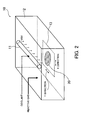
- FIG. 2 illustrates a principle of the chemical processor.
- the n-type semiconductor carbon nanomaterial can be produced using a chemical processor 10 having a structure as shown in FIG. 2 .
- This chemical processor 10 has a VUV lamp 11 which irradiates VUV and a reaction chamber 12 in which a carbon nanomaterial is placed.
- the VUV lamp 11 is designed to be cooled by an appropriate coolant.
- the reaction chamber 12 internally has a stage 13 for mounting thereon a substrate 20 on which a carbon nanomaterial is formed, for example, by a CVD (Chemical Vapor Deposition) method.
- This stage 13 has a moving mechanism movable in the X-Y directions, and a temperature controlling mechanism which controls a temperature of the mounted substrate 20.
- the reaction chamber 12 is designed to allow introduction of a gas (reactive gas) containing a substance having a functional group that serves as an electron-donating group when being bonded to the carbon nanomaterial.
- a gas reactive gas
- the substrate 20 is mounted on the stage 13 within the reaction chamber 12 and then, a reactive gas containing such a substance is introduced into the reaction chamber 12 under irradiation with VUV from the VUV lamp 11, thereby reacting the substance and the carbon nanomaterial on the substrate 20.
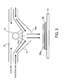
- FIG. 3 shows one example of a peripheral part of the VUV lamp 11.
- the chemical processor 10 has, for example, a structure as shown in FIG. 3 .
- a reactive gas introducing path 14 is provided which has a discharge port 14a formed opposite to the stage 13.
- the VUV lamp 11 is disposed near the side of the reactive gas introducing path 14 opposite to the discharge port 14a.
- a wall member of at least the VUV lamp 11 side of the reactive gas introducing path 14 is made of a material having high VUV transmittance, for example, a member transparent to VUV, such as silica glass, calcium fluoride (CaF 2 ) or magnesium fluoride (MgF 2 ).
- the entire of the reactive gas introducing path 14 may be made of such a material having high VUV transmittance.
- Examples of a lamp usable as the VUV lamp 11 include a Xe-filled excimer UV lamp that generates VUV at a peak wavelength of 172 nm.
- Various shapes of lamps can be used as the VUV lamp 11. For example, a cylindrical one can be used.
- a shape of the discharge port 14a of the reactive gas introducing path 14 is selected according to a shape of the VUV lamp 11 used.
- the VUV lamp 11 is disposed within a coolant passage 15 through which an appropriate coolant, for example, an inert gas such as argon (Ar) or N 2 absorbing no VUV is appropriately circulated to cool the VUV lamp 11.
- an appropriate coolant for example, an inert gas such as argon (Ar) or N 2 absorbing no VUV is appropriately circulated to cool the VUV lamp 11.
- processing for producing the n-type semiconductor carbon nanomaterial is performed as follows. First, the substrate 20 is mounted on the stage 13. Then, a reactive gas is introduced into the reactive gas introducing path 14 under irradiation with VUV from the VUV lamp 11.
- the reactive gas introduced is the above-described gaseous substance containing a substance having a predetermined functional group such as an amino group or an alkyl group. This substance is mixed with an inert gas and introduced into the reactive gas introducing path 14.
- the respective temperatures of the reactive gas, the reaction chamber 12 inside and the substrate 20 are suitably controlled according to reaction conditions.
- the reactive gas that circulates through the reactive gas introducing path 14 is activated, for example, by VUV irradiated through a wall member of the reactive gas introducing path 14 and generates radicals (amino radicals or alkyl radicals).
- the radicals are sprayed toward the substrate 20 from the discharge port 14a and the sprayed radicals react with a carbon nanomaterial 20a on the substrate 20 to thereby covalently bond a functional group such as an amino group or an alkyl group to the carbon nanomaterial 20a. If the carbon nanomaterial 20a has semiconductivity, since the bonded functional group serves as an electron-donating group, the semiconductor carbon nanomaterial 20a has n-type characteristics.
- FIG. 3 exemplifies a carbon nanotube as the carbon nanomaterial 20a on the substrate 20.
- the entire of the reactive gas introducing path 14 is made of a material having high VUV transmittance, energy can be supplied to the reactive gas discharged from the discharge port 14a or to the carbon nanomaterial 20a. As a result, a generation rate of radicals and a reaction rate of the carbon nanomaterial 20a can be improved.
- the above-described processing may be performed while moving the stage 13 having mounted thereon the substrate 20 in the X-Y directions according to a shape of the discharge port 14a to attain uniform processing.
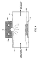
- FIG. 4 shows another example of the VUV lamp peripheral part.
- FIG. 4 exemplifies a graphene sheet as the carbon nanomaterial 20b on the substrate 20.
- the chemical processor 10 has, for example, a structure as shown in FIG. 4 .
- the VUV lamp 11 such as a Xe excimer UV lamp is disposed on the ceiling part of the reaction chamber 12 and provided with a cooling mechanism comprising a metal block 16 internally having a coolant passage 16a.
- the reaction chamber 12 is designed to allow circulation (introduction and discharge) of a reactive gas.
- the reactive gas that can be circulated is a mixture obtained by mixing the above-described substance having a functional group such as an amino group or an alkyl group with an inert gas.
- a liquid coolant such as water may be circulated in addition to an inert gas such as N 2 .
- processing for producing the n-type semiconductor carbon nanomaterial is performed as follows. First, the substrate 20 is mounted on the stage 13 within the reaction chamber 12. Then, a reactive gas is circulated within the reaction chamber 12 under irradiation with VUV from the VUV lamp 11. When circulating the reactive gas within the reaction chamber 12, the respective temperatures of the reactive gas, the reaction chamber 12 inside and the substrate 20 are suitably controlled according to reaction conditions.
- the reactive gas that circulates within the reaction chamber 12 is activated, for example, by VUV irradiation and generates radicals (amino radicals or alkyl radicals).
- the radicals react with the carbon nanomaterial 20b on the substrate 20 to thereby covalently bond a functional group such as an amino group or an alkyl group to the carbon nanomaterial 20b. If the carbon nanomaterial 20b has semiconductivity, since the bonded functional group serves as an electron-donating group, the semiconductor carbon nanomaterial 20b has n-type characteristics.
- the chemical processor 10 can be formed to have a relatively simple structure except for the VUV irradiation mechanism of the VUV lamp 11 peripheral part, so that the processing itself can be performed at low cost. Further, the reaction conditions can be relatively easily controlled, and inclusion of impurities during the processing can be prevented. As a result, an n-type semiconductor carbon nanomaterial having high reliability can be stably produced.
- an introduction temperature of the reactive gas to a temperature where a substance having a functional group such as an amino group or an alkyl group is vaporized or isolated near a sample, for example, a temperature lower than the boiling point of the substance by about 10 to 50°C.
- a substance having a functional group such as an amino group or an alkyl group
- n-type semiconductor carbon nanomaterial when producing the n-type semiconductor carbon nanomaterial using the chemical processor 10, physical and chemical properties (for example, device characteristics of a semiconductor device such as a transistor manufactured by using the n-type semiconductor carbon nanomaterial, or chemical characteristics of the n-type semiconductor carbon nanomaterial) of the resulting n-type semiconductor carbon nanomaterial can be controlled in detail by changing a type of the substance used as the reactive gas without changing the basic procedures.
- the reaction conditions can be controlled. Further, various n-type semiconductor carbon nanomaterials having different characteristics can be separately produced.
- the reactive gas a mixed gas obtained by diluting the above-described substance having a functional group such as an amino group or an alkyl group with an inert gas.
- the above-described substance having a functional group suitable for this chemical processing often has a large VUV absorption coefficient. Further, the VUV have large absorption coefficients in air and therefore, are often absorbed within a distance of from 1 to several centimeters from a light source.
- a concentration of this substance in the mixed gas is set, for example, between 0.0001 and 50%, preferably between 0.01 and 10%.
- the concentration is set based on a type of the substance, an introduction temperature of the reactive gas, a temperature within the reaction chamber 12, a temperature of the substrate 20, and other various reaction conditions.
- a dry process is used for producing the n-type semiconductor carbon nanomaterial. Specifically, a semiconductor carbon nanomaterial is reacted with a gaseous substance containing a substance having a functional group serving as an electron-donating group to thereby covalently bond the functional group to a specific site of the carbon nanomaterial.
- the n-type semiconductor carbon nanomaterial can be produced at low cost using a relatively simple processor.
- inclusion of impurities can be effectively suppressed and an environmental load can be reduced as compared with the production of the n-type semiconductor carbon nanomaterial by a wet process. Further, although the wet process has failed to eliminate particularly the problem of bundling of carbon nanotubes during the processing, the above-described dry process can eliminate such a trouble during the processing.
- the n-type semiconductor carbon nanomaterial having high reliability can be simply and stably produced at low cost.
- the structure of a reactive substance or the reaction conditions employed when using the reactive substance can be finely changed and thereby, the reaction or the characteristics of the n-type semiconductor carbon nanomaterial can be controlled.
- the chemical processor 10 can produce an n-type semiconductor carbon nanomaterial and at the same time, can also produce a p-type semiconductor carbon nanomaterial.
- a reactive gas is introduced which has various functional groups (electron-withdrawing groups) in place of the above-described electron-donating groups and which exhibits an electron-withdrawing property when being bonded to the carbon nanomaterial.
- the substance and a carbon nanomaterial on the substrate 20 are reacted under irradiation with VUV from the VUV lamp 11 to thereby form a covalent bond between the electron-withdrawing group and the carbon nanomaterial.
- the electron-withdrawing group bonded to the carbon nanomaterial draws electrons from the carbon nanomaterial through the covalent bond and imparts p-type characteristics to the semiconductor carbon nanomaterial.
- the p-type semiconductor carbon nanomaterial can be produced.
- the covalent bond formed between the electron-withdrawing group and the carbon nanomaterial is stable and low reactive. Therefore, the p-type semiconductor carbon nanomaterial thus covalently bonded with the electron-withdrawing group has a property of hardly changing over time, that is, a property of preserving p-type semiconductor characteristics.
- 1% oxygen gas is introduced as the reactive gas. Then, the oxygen gas and the graphene sheet are reacted under irradiation with VUV in the same manner as in the above-described example and thereby, a carboxyl group (-COOH group) as an electron-withdrawing group is covalently bonded to a specific site, particularly, to a specific site of the surface of the graphene sheet.
- a carboxyl group (-COOH group) as an electron-withdrawing group is covalently bonded to a specific site, particularly, to a specific site of the surface of the graphene sheet.
- a method for producing the n-type semiconductor carbon nanomaterial by a dry process is described above. This method can be easily applied to an FET fabrication process.
- an n-channel FET is fabricated by the following process. First, a semiconductor carbon nanomaterial is formed over a region (channel region) serving as a channel between the source electrode and the drain electrode. Then, the semiconductor carbon nanomaterial is reacted with a gaseous substance containing a substance having a predetermined functional group to produce an n-type semiconductor carbon nanomaterial, and the produced n-type semiconductor carbon nanomaterial is used as a channel.
- This method can be applied to fabrication of any of the n-channel FETs having a top-gate structure and a back-gate structure as exemplified above.
- device stabilization may be achieved by forming a passivation film on a surface at an appropriate stage according to the structure of the n-channel FET.
- Materials and forming conditions of the passivation film are not particularly limited as long as they do not cause any deterioration of the carbon nanomaterial.
- the above-described p-type semiconductor carbon nanomaterial can be applied to the FET.
- FIGS. 5A and 5B show structure examples of a top-gate carbon nanomaterial FET.
- FIG. 5A is a schematic perspective view and
- FIG. 5B is a schematic cross-sectional view.
- An n-channel FET 30 shown in FIG. 5 comprises an insulating substrate, for example, a sapphire substrate 31, a source electrode 32 formed on the sapphire substrate 31 and having a catalytic action, a drain electrode 33 formed on the sapphire substrate 31 so as to face the source electrode 32, and n-type semiconductor carbon nanomaterials 34 formed over channel regions between the source electrode 32 and the drain electrode 33.
- the n-type semiconductor carbon nanomaterials 34 are covered with an insulating film, for example, an SOG (Spin On Glass) film 35. Portions of the SOG film 35, which cover the surface of the n-type semiconductor carbon nanomaterial 34, act as a gate insulating film 35a, and a gate electrode 36 is formed on the gate insulating film 35a. Further, an earth electrode 37 is formed on the back surface of the sapphire substrate 31.
- FIG. 5 shows the case where the n-type semiconductor carbon nanomaterials 34 are n-type semiconductor carbon nanotubes.
- a layer below the n-type semiconductor carbon nanomaterials 34 must be an SOG film or other insulating materials such as an insulator.
- the n-channel FET 30 having the above-described structure can be fabricated, for example, through processes as shown in the following FIGS. 6 to 14 .
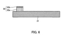
- FIG. 6 is a schematic cross-sectional view of a process for forming a source electrode.
- FIG. 7 is a schematic cross-sectional view of a process for forming a drain electrode.
- FIG. 8 is a schematic cross-sectional view of a process for growing a semiconductor carbon nanotube.
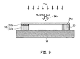
- FIG. 9 is a schematic cross-sectional view of a process for producing an n-type semiconductor carbon nanotube.
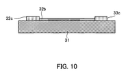
- FIG. 10 is a schematic cross-sectional view of a process for forming a source electrode and a drain electrode.
- FIG. 11 is a schematic cross-sectional view of processes for growing a semiconductor graphene sheet and for producing an n-type semiconductor graphene sheet.
- FIG. 12 is a schematic cross-sectional view of a process for forming an insulating film.
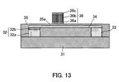
- FIG. 13 is a schematic cross-sectional view of a process for forming a gate electrode.
- the production process of the carbon nanomaterials formed between the source electrode 32 and the drain electrode 33 depends on either carbon nanotubes or graphene sheets. Each production process of the carbon nanotubes and the graphene sheets will be described below.
- an aluminum (Al) film 32a having, for example, a thickness of 5 nm and an iron (Fe) film 32b having, for example, a thickness of 1 nm are sequentially deposited over the sapphire substrate 31 by a sputtering method using a resist pattern (not shown in the figure) as a mask. Thereafter, the resist pattern is removed. Thus, the source electrode 32 is formed.
- the Fe film 32b acts as a catalyst during the growth of a carbon nanotube 34a.
- an Al film having, for example, a thickness of 6 nm is deposited so as to face the source electrode 32 while leaving a space of, for example, 5 ⁇ m therebetween. Thereafter, the resist pattern is removed. Thus, the drain electrode 33 is formed.
- a plurality of carbon nanotubes 34a are grown while applying a DC electric field between the source electrode 32 and the drain electrode 33 (channel region), for example, under a pressure of 100 Pa and a growth temperature of 600°C.
- the Fe film 32b constituting the surface of the source electrode 32 is broken into particles under the influence of temperature and the particle diameter is reduced in a reflection of the wettability with the lower Al film 32a.
- the grown carbon nanotubes 34a form into semiconductor single wall carbon nanotubes.
- the carbon nanotubes 34a In the growth process, since the DC electric field is applied between the source electrode 32 and the drain electrode 33, the carbon nanotubes 34a begin to grow toward the drain electrode 33 from the upper Fe film 32b of the source electrode 32. Then, the carbon nanotubes 34a complete the growth when sufficiently reaching the drain electrode 33.
- the growth time is, for example, 40 minutes.
- the grown semiconductor carbon nanotubes 34a are reacted with a reactive gas 34b containing the above-described substance having a predetermined functional group, for example, under irradiation with VUV to thereby produce the n-type semiconductor carbon nanotubes 34a serving as channels.
- the chemical processor 10 having the above-described structure can be used.
- a gold (Au) film having, for example, a thickness of 3 nm is deposited on an insulator, for example, on the sapphire substrate 31 by a sputtering method using a resist pattern (not shown in the figure) as a mask. Thereafter, the resist pattern is removed. Thus, a source electrode 32c and a drain electrode 33c are formed while leaving a space of, for example, 5 ⁇ m therebetween and the Fe film 32b having, for example, a thickness of 1 nm is formed between the source electrode 32c and the drain electrode 33c.
- graphene sheets 34c are grown by a conventionally known method using the Fe film 32b as a catalyst. Then, the grown semiconductor graphene sheets 34c are reacted with the reactive gas 34b under irradiation with VUV in the same manner as in the case of producing the n-type carbon nanotubes 34a by the chemical processor 10. Thus, the n-type semiconductor graphene sheets 34c are produced.
- the n-type semiconductor carbon nanomaterial 34 is produced between the source electrode 32 and the drain electrode 33 in the n-channel FET 30.
- the following production process can be applied commonly to the carbon nanotubes 34a and the graphene sheets 34c.
- the production process subsequent to FIG. 9 will be described below.
- the SOG film 35 is deposited to have, for example, a thickness of 10 nm on the surface of the n-type semiconductor carbon nanomaterial 34 so as to cover the n-type semiconductor carbon nanomaterial 34 by a spin coat method and an annealing method, thereby forming as the gate insulating film 35a a portion deposited on the n-type semiconductor carbon nanomaterial 34.
- a titanium (Ti) film 36a having, for example, a thickness of 10 nm, a platinum (Pt) film 36b having, for example, a thickness of 100 nm, and a titanium (Ti) film 36c having, for example, a thickness of 10 nm are sequentially deposited by a sputtering method using a resist pattern (not shown in the figure) as a mask. Thereafter, the resist pattern is removed. Thus, the gate electrode 36 is formed.
- the earth electrode 37 made of aluminum is provided on the back surface of the sapphire substrate 31.
- the n-channel FET 30 having a structure shown in FIG. 5 is fabricated.
- FIGS. 14A and 14B show structure examples of a back-gate carbon nanomaterial FET.
- FIG. 14A is a schematic perspective view and
- FIG. 14B is a schematic cross-sectional view.
- An n-channel FET 40 shown in FIG. 14 uses as a gate electrode a conductive substrate, for example, a highly doped silicon (Si) substrate 41.
- a back-gate metal layer 42 using Ti or Pt is provided on one surface (back surface) of the Si substrate 41.
- a silicon oxide (SiO 2 ) film 43 serving as a gate insulating film is provided on another surface (surface) thereof.
- a source electrode 44 having a catalytic action and a drain electrode 45 are provided to face each other while leaving a predetermined space therebetween (a catalytic layer is not shown in the figure).
- N-type semiconductor carbon nanomaterials 46 serving as a channel are provided between the source electrode 44 and the drain electrode 45.
- the n-type semiconductor carbon nanomaterials 46 are covered with a passivation film 47.
- the n-channel FET 40 having the above-described structure is fabricated, for example, by the following process.
- the SiO 2 film 43 is formed on the surface of the Si substrate 41.
- the source electrode 44 having a layered structure of, for example, a Fe film and an Al film and the drain electrode 45 are formed on the SiO 2 film 43.
- the semiconductor carbon nanomaterials are grown between the source electrode 44 and the drain electrode 45 (channel region). At this time, both ends of the carbon nanomaterials may be formed on the upper surfaces of the source electrode 44 and the drain electrode 45, respectively (not shown in the figure).
- the thus formed semiconductor carbon nanomaterials are reacted with a reactive gas containing the above-described substance having a predetermined functional group, for example, under irradiation with VUV to thereby produce the n-type semiconductor carbon nanomaterials 46 serving as channels.
- a reactive gas containing the above-described substance having a predetermined functional group for example, under irradiation with VUV to thereby produce the n-type semiconductor carbon nanomaterials 46 serving as channels.
- the chemical processor 10 having the above-described structure can be used.
- the n-channel FET 40 having a structure shown in FIG. 15 is fabricated.
- a complementary FET using semiconductor carbon nanomaterials is fabricated, for example, by the following process.
- the semiconductor carbon nanomaterials are formed over the channel regions disposed between regions for fabricating a p-channel FET and an n-channel FET, respectively.
- a region for fabricating the p-channel FET is masked and a region for fabricating the n-channel FET is exposed using a photolithography method.
- the carbon nanomaterials formed on the n-channel FET side are reacted with a gaseous substance containing a substance having a predetermined functional group to thereby produce the n-type semiconductor carbon nanomaterials.
- the p-type semiconductor carbon nanomaterials are formed on the p-channel FET side and the n-type semiconductor carbon nanomaterials are formed on the n-channel FET side, so that the p-type and n-type channels can be separately formed.
- This method can be applied to fabrication of any of the complementary FETs having a top-gate structure and a back-gate structure as exemplified above.
- the above-described separate formation method can be similarly applied to a case of fabricating plural types of FETs using, as channels, the n-type semiconductor carbon nanomaterials having different characteristics. Further, this method can be similarly applied to a case of mixedly mounting a FET using carbon nanomaterials and a FET not using carbon materials on the same substrate.
- n-type semiconductor carbon nanomaterials production of n-type semiconductor carbon nanotubes and n-type semiconductor graphene sheets by the above-described dry process will be described below, respectively.
- the carbon nanotube to be processed may be a single wall carbon nanotube (SWNT), a double wall carbon nanotube (DWNT), or a multi wall carbon nanotube (MMNT). Further, all forms of carbon nanotubes suitable for the manufacturing process of a semiconductor device, such as a carbon nanotube directly grown on the substrate or a carbon nanotube produced by applying or dispersing the formed carbon nanotube on the substrate, can be used as the carbon nanotube to be processed.
- SWNT single wall carbon nanotube
- DWNT double wall carbon nanotube
- MMNT multi wall carbon nanotube
- the above-described chemical processor 10 shown in FIGS. 2 and 3 is used.
- the chemical processor 10 has a Xe excimer UV lamp as the VUV lamp 11 that generates VUV with an output of 30 mW/cm 2 , an emission wavelength of 400 nm, and a peak wavelength of 172 nm.
- An Si wafer (p type, (100) surface) with about 1.5 ⁇ m of MWNTs formed thereon is used as a sample.
- a nickel (Ni) film is formed on the Si wafer to a thickness of 25 nm by a sputtering method and then the MWNTs are grown by thermal filament CVD method at 650°C using C 2 H 2 gas as the raw material.
- This sample is baked at 400°C for about 15 minutes in air to previously remove combustible impurities other than carbon nanomaterials and is then transferred immediately to the chemical processor 10. Thereafter, using as a reactive gas a gaseous substance obtained by diluting (CH 3 CH 2 ) 3 N with pure nitrogen to a vapor pressure of 1 atmosphere and an oxygen concentration of about 5 vol%, processing of the MWNTs on the Si wafer is performed by introducing the reactive gas into the reactive gas introducing path 14 at a flow rate of 1L per minute.
- a reactive gas a gaseous substance obtained by diluting (CH 3 CH 2 ) 3 N with pure nitrogen to a vapor pressure of 1 atmosphere and an oxygen concentration of about 5 vol%
- the sample before and after this processing is analyzed by an X-ray Photoelectron Spectroscopy (XPS) and an Infrared Spectroscopy (IR).
- XPS X-ray Photoelectron Spectroscopy
- IR Infrared Spectroscopy
- the same chemical processor 10 as that used in the first embodiment is used, and an Si wafer (p-type, (100) surface) with SWNTs formed thereon is used as a sample.
- the SWNTs are produced on the Si wafer by arc discharge. Thereafter, the baking process is performed under the same conditions as those of the first embodiment.
- processing of the SWNTs on the Si wafer is performed by introducing into the reactive gas introducing path 14 a reactive gas having the same composition and flow rate as those of the reactive gas in the first embodiment. Note, however, that the processing time is 10% of that in the processing of the MWNTs.
- the sample before and after this processing is analyzed by the XPS and the IR. As a result, it is confirmed that C-N bonds not present in the SWNTs before the processing are formed after the processing.
- the same chemical processor 10 as that used in the second embodiment is used, and an FET comprising a channel composed of SWNTs is used as a sample.
- processing of the SWNTs is performed by introducing into the reactive gas introducing path 14 a reactive gas having the same composition and flow rate as those of the reactive gases in the first and second embodiments.
- the sample before and after this processing is analyzed by the XPS and the IR. As a result, it is confirmed that the SWNTs exhibiting weak p-type characteristics before the processing develop n-type characteristics after the processing. Further, it is confirmed that the SWNTs exhibit the n-type characteristics not only immediately after the processing but also continuously.
- the above-described chemical processor 10 shown in FIGS. 2 and 4 is used.
- the chemical processor 10 has a Xe excimer UV lamp as the VUV lamp 11 that generates VUV with an output of 30 mW/cm 2 , an emission wavelength of 400 nm, and a peak wavelength of 172 nm.
- An Si wafer (p type, (100) surface) with about 10 ⁇ m of MWNTs formed thereon is used as a sample.
- a nickel (Ni) film is formed on the Si wafer to a thickness of 25 nm by a sputtering method and then the MWNTs are grown by thermal filament CVD method at 650°C using C 2 H 2 gas as the raw material.
- This sample is baked at 400°C for 15 minutes in air to previously remove combustible impurities other than carbon nanomaterials and is then transferred immediately to the chemical processor 10. Thereafter, using as a reactive gas a gaseous substance obtained by diluting ethanol (CH 3 CH 2 OH) with pure nitrogen to a vapor partial pressure of about 1%, processing of the MWNTs on the Si wafer is performed by introducing the reactive gas into the reaction chamber 12 at a flow rate of 1L per minute.
- a reactive gas a gaseous substance obtained by diluting ethanol (CH 3 CH 2 OH) with pure nitrogen to a vapor partial pressure of about 1%
- the sample before and after this processing is analyzed by the XPS and the IR. As a result, it is confirmed that a hydroxyl group (0.1% or less) scarcely present in the MWNTs before the processing is formed to be about 2% in terms of a carbon element ratio after the processing.
- the same chemical processor 10 as that used in the fourth embodiment is used, and an Si wafer (p-type, (100) surface) with SWNTs formed thereon is used as a sample.
- the SWNTs are produced on the Si wafer by arc discharge. Thereafter, the baking process is performed under the same conditions as those of the fourth embodiment.
- processing of the SWNTs on the Si wafer is performed by introducing into the reaction chamber 12 a reactive gas having the same composition and flow rate as those of the reactive gas in the fourth embodiment. Note, however, that the processing time is 10% of that in the processing of the MWNTs.
- the sample before and after this processing is analyzed by the XPS and the IR. As a result, it is confirmed that a hydroxyl group scarcely present in the MWNTs before the processing is formed to be about 2% in terms of a carbon element ratio after the processing.
- the same chemical processor 10 as that used in the fifth embodiment is used, and an FET comprising a channel composed of SWNTs is used as a sample.
- processing of the SWNTs on the Si wafer is performed by introducing into the reaction chamber 12 a reactive gas having the same composition and flow rate as those of the reactive gases in the fourth and fifth embodiments.
- the sample before and after this processing is analyzed by the XPS and the IR. As a result, it is confirmed that the SWNTs exhibiting weak p-type characteristics before the processing develop n-type characteristics after the processing. Further, it is confirmed that the SWNTs exhibit the n-type characteristics not only immediately after the processing but also continuously.
- Graphene sheets are inexpensive and stable because of having large electron mobility and no bundle. Further, graphene sheets are easily processed and easily integrated into a planar transistor as compared with carbon nanotubes.
- the graphene sheet to be processed may be a single-layered or multi-layered graphene sheet. Further, all forms of graphene sheets suitable for the manufacturing process of the semiconductor device, such as a graphene sheet directly grown on the substrate or a graphene sheet produced by applying or dispersing the formed graphene sheet on the substrate, can be used as the graphene sheet to be processed.
- the processing of the graphene sheets in place of the carbon nanotubes is performed in the same manner as in the above-described embodiments. Then, the sample before and after the processing is analyzed by the XPS and the IR in the same manner as in the above-described embodiments. As a result, it is confirmed that the n-type graphene sheet is produced.
Landscapes
- Chemical & Material Sciences (AREA)
- Engineering & Computer Science (AREA)
- Nanotechnology (AREA)
- Materials Engineering (AREA)
- Organic Chemistry (AREA)
- Inorganic Chemistry (AREA)
- Crystallography & Structural Chemistry (AREA)
- Physics & Mathematics (AREA)
- General Physics & Mathematics (AREA)
- Condensed Matter Physics & Semiconductors (AREA)
- Theoretical Computer Science (AREA)
- Composite Materials (AREA)
- Mathematical Physics (AREA)
- Manufacturing & Machinery (AREA)
- Carbon And Carbon Compounds (AREA)
- Thin Film Transistor (AREA)
Applications Claiming Priority (2)
| Application Number | Priority Date | Filing Date | Title |
|---|---|---|---|
| PCT/JP2006/316307 WO2008023399A1 (en) | 2006-08-21 | 2006-08-21 | n-TYPE SEMICONDUCTOR CARBON NANOTUBES, PROCESS FOR PRODUCTION THEREOF, AND PROCESS FOR PRODUCTION OF SEMICONDUCTOR DEVICES |
| PCT/JP2007/066131 WO2008023669A1 (en) | 2006-08-21 | 2007-08-20 | n-TYPE SEMICONDUCTOR CARBON NANOMATERIAL, METHOD FOR PRODUCING n-TYPE SEMICONDUCTOR CARBON NANOMATERIAL, AND METHOD FOR MANUFACTURING SEMICONDUCTOR DEVICE |
Publications (2)
| Publication Number | Publication Date |
|---|---|
| EP2055672A1 true EP2055672A1 (de) | 2009-05-06 |
| EP2055672A4 EP2055672A4 (de) | 2010-10-13 |
Family
ID=39106493
Family Applications (1)
| Application Number | Title | Priority Date | Filing Date |
|---|---|---|---|
| EP07792744A Withdrawn EP2055672A4 (de) | 2006-08-21 | 2007-08-20 | N-halbleiter-kohlenstoffnanomaterial, verfahren zur herstellung von n-halbleiter-kohlenstoffnanomaterial und verfahren zur herstellung einer halbleitervorrichtung |
Country Status (4)
| Country | Link |
|---|---|
| US (1) | US20090221130A1 (de) |
| EP (1) | EP2055672A4 (de) |
| KR (1) | KR20090039749A (de) |
| WO (2) | WO2008023399A1 (de) |
Cited By (3)
| Publication number | Priority date | Publication date | Assignee | Title |
|---|---|---|---|---|
| CN101774575A (zh) * | 2010-02-10 | 2010-07-14 | 中国科学院上海硅酸盐研究所 | 低温下用含氨基基团的有机物修复氧化后的石墨烯的方法 |
| WO2017041171A1 (en) * | 2015-09-08 | 2017-03-16 | Grafoid Inc. | Process for coating a substrate with a carbon-based material |
| CN107017285A (zh) * | 2015-12-02 | 2017-08-04 | 三星电子株式会社 | 场效应晶体管以及包括该场效应晶体管的半导体器件 |
Families Citing this family (32)
| Publication number | Priority date | Publication date | Assignee | Title |
|---|---|---|---|---|
| JP5470610B2 (ja) * | 2007-10-04 | 2014-04-16 | 国立大学法人福井大学 | グラフェンシートの製造方法 |
| JP2009234815A (ja) * | 2008-03-26 | 2009-10-15 | Fujitsu Ltd | グラフェンシート系材料の処理方法及び装置 |
| KR101450591B1 (ko) * | 2008-06-05 | 2014-10-17 | 삼성전자주식회사 | 탄소나노튜브 엔 도핑 물질 및 방법, 이를 이용한 소자 |
| JP5453045B2 (ja) * | 2008-11-26 | 2014-03-26 | 株式会社日立製作所 | グラフェン層が成長された基板およびそれを用いた電子・光集積回路装置 |
| KR101156620B1 (ko) * | 2009-04-08 | 2012-06-14 | 한국전자통신연구원 | 그라핀 채널층을 가지는 전계 효과 트랜지스터 |
| CN104934300B (zh) * | 2009-11-13 | 2018-08-14 | 富士通株式会社 | 半导体装置及其制造方法 |
| JP5708493B2 (ja) * | 2009-11-13 | 2015-04-30 | 富士通株式会社 | 半導体装置及びその製造方法 |
| JP2011175996A (ja) * | 2010-02-23 | 2011-09-08 | Nippon Telegr & Teleph Corp <Ntt> | グラフェントランジスタおよびその製造方法 |
| JP2011192667A (ja) * | 2010-03-11 | 2011-09-29 | Toshiba Corp | トランジスタおよびその製造方法 |
| US8946903B2 (en) * | 2010-07-09 | 2015-02-03 | Micron Technology, Inc. | Electrically conductive laminate structure containing graphene region |
| EP2602830A4 (de) | 2010-08-05 | 2017-03-22 | Fujitsu Limited | Verfahren zur herstellung von halbleiterbauelementen und verfahren zur graphenzüchtung |
| JP2012036040A (ja) * | 2010-08-06 | 2012-02-23 | Fujitsu Ltd | グラフェンシート系材料の形成方法およびグラフェンシート系材料 |
| US8344358B2 (en) * | 2010-09-07 | 2013-01-01 | International Business Machines Corporation | Graphene transistor with a self-aligned gate |
| JP5904734B2 (ja) | 2010-09-16 | 2016-04-20 | 三星電子株式会社Samsung Electronics Co.,Ltd. | グラフェン発光素子及びその製造方法 |
| KR101715355B1 (ko) * | 2010-11-30 | 2017-03-13 | 삼성전자주식회사 | 그래핀 전자 소자 |
| US8354296B2 (en) * | 2011-01-19 | 2013-01-15 | International Business Machines Corporation | Semiconductor structure and circuit including ordered arrangement of graphene nanoribbons, and methods of forming same |
| KR101469450B1 (ko) * | 2011-03-02 | 2014-12-05 | 그래핀스퀘어 주식회사 | 그래핀의 n-도핑 방법 |
| JP5978600B2 (ja) * | 2011-11-21 | 2016-08-24 | 富士通株式会社 | 半導体装置の製造方法 |
| KR102037469B1 (ko) * | 2012-01-02 | 2019-10-28 | 삼성전자주식회사 | 그래핀 전자 소자 및 그 제조 방법 |
| JP5510522B2 (ja) * | 2012-09-27 | 2014-06-04 | 富士通株式会社 | グラフェンシート系材料の処理方法 |
| US9178032B2 (en) * | 2013-02-15 | 2015-11-03 | Electronics And Telecommunications Research Institute | Gas sensor and manufacturing method thereof |
| CN103745994A (zh) * | 2013-12-24 | 2014-04-23 | 上海新傲科技股份有限公司 | 采用石墨烯的场效应晶体管及其制备方法 |
| EP3163639B1 (de) | 2014-06-26 | 2021-03-17 | National University Corporation Nara Institute of Science and Technology | Verwendung einer dotierstoffzusammensetzung zur änderung des seebeck-koeffizientes eines nanomaterials |
| JP6394301B2 (ja) * | 2014-11-10 | 2018-09-26 | 富士通株式会社 | ガスセンサ及びその製造方法 |
| KR101911745B1 (ko) * | 2015-03-23 | 2018-10-25 | 재단법인 나노기반소프트일렉트로닉스연구단 | 그래핀 적층체 및 그의 제조방법 |
| CN106226377A (zh) * | 2016-07-06 | 2016-12-14 | 无锡盈芯半导体科技有限公司 | 一种基于石墨烯的场效应晶体管生物传感器及其制备方法 |
| KR101957825B1 (ko) | 2017-01-31 | 2019-07-04 | 주식회사 협진기계 | 스파이럴 오븐기용 열기 순환장치 |
| KR101894893B1 (ko) | 2017-01-31 | 2018-09-04 | 주식회사 협진기계 | 스파이럴 오븐기용 가열장치 |
| KR101910427B1 (ko) | 2017-02-13 | 2018-10-22 | 주식회사 협진기계 | 스파이럴 오븐기용 세척장치 |
| JP6485593B2 (ja) * | 2017-03-27 | 2019-03-20 | 東レ株式会社 | 半導体素子、相補型半導体装置、半導体素子の製造方法、無線通信装置および商品タグ |
| KR20200037541A (ko) | 2018-10-01 | 2020-04-09 | 주식회사 협진기계 | 가스타입의 스파이럴 오븐기 |
| KR102389395B1 (ko) * | 2020-06-18 | 2022-04-20 | 국민대학교산학협력단 | Cnt를 포함하는 비휘발성 메모리 소자, cnt를 포함하는 비휘발성 메모리 소자 제조 방법 및 웨어러블 장치 |
Family Cites Families (15)
| Publication number | Priority date | Publication date | Assignee | Title |
|---|---|---|---|---|
| US6835366B1 (en) * | 1998-09-18 | 2004-12-28 | William Marsh Rice University | Chemical derivatization of single-wall carbon nanotubes to facilitate solvation thereof, and use of derivatized nanotubes |
| EP1186572A1 (de) * | 2000-09-06 | 2002-03-13 | Facultés Universitaires Notre-Dame de la Paix | Kurze Kohlenstoffnanoröhren und Verfahren zu deren Herstellung |
| GB2389847B (en) | 2001-01-29 | 2005-08-10 | Univ Rice William M | Process for derivatizing carbon nanotubes with diazonium species and compositions thereof |
| TWI220269B (en) * | 2002-07-31 | 2004-08-11 | Ind Tech Res Inst | Method for fabricating n-type carbon nanotube device |
| JP4545373B2 (ja) | 2002-11-07 | 2010-09-15 | 旭化成株式会社 | 有機半導体薄膜及びその製造方法 |
| JP3764986B2 (ja) | 2002-11-18 | 2006-04-12 | 独立行政法人科学技術振興機構 | 可溶性カーボンナノチューブの製造法 |
| JP3781732B2 (ja) * | 2003-03-20 | 2006-05-31 | 株式会社東芝 | カーボンナノチューブの製造方法、カーボンナノチューブを用いた半導体装置の製造方法、及びカーボンナノチューブの製造装置 |
| US7670831B2 (en) | 2003-06-13 | 2010-03-02 | Korea Advanced Institute Of Science And Technology | Conductive carbon nanotubes dotted with metal and method for fabricating a biosensor using the same |
| JP4834950B2 (ja) | 2003-09-12 | 2011-12-14 | ソニー株式会社 | 電界効果半導体装置の製造方法 |
| JP2005272184A (ja) * | 2004-03-23 | 2005-10-06 | Honda Motor Co Ltd | 親水性カーボンナノチューブの製造方法 |
| JP4515798B2 (ja) * | 2004-03-24 | 2010-08-04 | 本田技研工業株式会社 | カーボンナノチューブ強化複合材料の製造方法 |
| JP2006049435A (ja) * | 2004-08-02 | 2006-02-16 | Sony Corp | カーボンナノチューブ及びその配置方法と、これを用いた電界効果トランジスタとその製造方法及び半導体装置 |
| JP4779172B2 (ja) * | 2005-01-06 | 2011-09-28 | 独立行政法人産業技術総合研究所 | ドーピングされたカーボンナノチューブ及びその製造方法 |
| JP2006213569A (ja) * | 2005-02-04 | 2006-08-17 | Tokyo Institute Of Technology | 表面処理カーボンナノファイバーおよびその製造方法 |
| KR100668352B1 (ko) * | 2006-01-05 | 2007-01-12 | 삼성전자주식회사 | 질소 도핑된 단일벽 탄소나노튜브의 제조방법 |
-
2006
- 2006-08-21 WO PCT/JP2006/316307 patent/WO2008023399A1/ja not_active Ceased
-
2007
- 2007-08-20 EP EP07792744A patent/EP2055672A4/de not_active Withdrawn
- 2007-08-20 WO PCT/JP2007/066131 patent/WO2008023669A1/ja not_active Ceased
- 2007-08-20 KR KR1020097002556A patent/KR20090039749A/ko not_active Ceased
-
2009
- 2009-02-02 US US12/364,018 patent/US20090221130A1/en not_active Abandoned
Cited By (4)
| Publication number | Priority date | Publication date | Assignee | Title |
|---|---|---|---|---|
| CN101774575A (zh) * | 2010-02-10 | 2010-07-14 | 中国科学院上海硅酸盐研究所 | 低温下用含氨基基团的有机物修复氧化后的石墨烯的方法 |
| WO2017041171A1 (en) * | 2015-09-08 | 2017-03-16 | Grafoid Inc. | Process for coating a substrate with a carbon-based material |
| US10710113B2 (en) | 2015-09-08 | 2020-07-14 | Grafoid, Inc. | Process for coating a substrate with a carbon-based material |
| CN107017285A (zh) * | 2015-12-02 | 2017-08-04 | 三星电子株式会社 | 场效应晶体管以及包括该场效应晶体管的半导体器件 |
Also Published As
| Publication number | Publication date |
|---|---|
| WO2008023399A1 (en) | 2008-02-28 |
| US20090221130A1 (en) | 2009-09-03 |
| KR20090039749A (ko) | 2009-04-22 |
| WO2008023669A1 (en) | 2008-02-28 |
| EP2055672A4 (de) | 2010-10-13 |
Similar Documents
| Publication | Publication Date | Title |
|---|---|---|
| EP2055672A1 (de) | N-halbleiter-kohlenstoffnanomaterial, verfahren zur herstellung von n-halbleiter-kohlenstoffnanomaterial und verfahren zur herstellung einer halbleitervorrichtung | |
| Sovizi et al. | Plasma processing and treatment of 2D transition metal dichalcogenides: tuning properties and defect engineering | |
| US8951609B2 (en) | CNT devices, low-temperature fabrication of CNT and CNT photo-resists | |
| Shi et al. | Recent advances in controlled synthesis of two-dimensional transition metal dichalcogenides via vapour deposition techniques | |
| Kim et al. | Fermi level engineering of single-walled carbon nanotubes by AuCl3 doping | |
| US9637839B2 (en) | Synthesis and transfer of metal dichalcogenide layers on diverse surfaces | |
| EP2298697B1 (de) | Verfahren zur herstellung eines kohlenstoffdrahts und einer leitfähigen folie | |
| Peng et al. | Single-walled carbon nanotubes templated CuO networks for gas sensing | |
| CN1903715B (zh) | 制造碳纳米管的聚集体与薄膜、电子元件、破坏碳纳米管以及碳纳米管的选择性反应的方法 | |
| US20150064471A1 (en) | Seed for Metal Dichalcogenide Growth by Chemical Vapor Deposition | |
| Jung et al. | Effect of ultraviolet-ozone treatment on MoS2 monolayers: comparison of chemical-vapor-deposited polycrystalline thin films and mechanically exfoliated single crystal flakes | |
| Yu et al. | Flexible photodetectors with single-crystalline GaTe nanowires | |
| CN113913940B (zh) | 一种一维双层二硫化钨水平纳米带的制备方法 | |
| US20180009664A1 (en) | Method for synthesizing carbon materials from carbon agglomerates containing carbine/carbynoid chains | |
| Kimura et al. | Electron affinity and field emission characteristics of boron carbon nitride film | |
| Li et al. | Selective synthesis of large diameter, highly conductive and high density single-walled carbon nanotubes by a thiophene-assisted chemical vapor deposition method on transparent substrates | |
| Li et al. | Growth and electrical properties of n-type monolayer sulfur-doped graphene film in air | |
| Yang et al. | Formation of diamond-like carbon films by photoemission-assisted plasma-enhanced chemical vapor deposition | |
| Ong et al. | Patterned growth of vertically-aligned ZnO nanorods on a flexible platform for feasible transparent and conformable electronics applications | |
| Wu et al. | Three step fabrication of graphene at low temperature by remote plasma enhanced chemical vapor deposition | |
| Feng et al. | Recent Advances of Plasma Technology Applications in 2D Materials and Electronics | |
| JP5099010B2 (ja) | n型半導体カーボンナノ材料の製造方法および半導体装置の製造方法 | |
| Hatakeyama et al. | Plasma processing based synthesis of functional Nanocarbons | |
| Wu et al. | Oxidant‐Modulated Synthesis of Polycrystalline MoS2 on SiO2/Si With Near‐Single‐Crystal Mobility | |
| Cha et al. | Selective and local flash-annealing for improvement in the contact characteristics of MoS 2 transistors |
Legal Events
| Date | Code | Title | Description |
|---|---|---|---|
| PUAI | Public reference made under article 153(3) epc to a published international application that has entered the european phase |
Free format text: ORIGINAL CODE: 0009012 |
|
| 17P | Request for examination filed |
Effective date: 20090202 |
|
| AK | Designated contracting states |
Kind code of ref document: A1 Designated state(s): DE FR |
|
| DAX | Request for extension of the european patent (deleted) | ||
| RBV | Designated contracting states (corrected) |
Designated state(s): DE FR |
|
| A4 | Supplementary search report drawn up and despatched |
Effective date: 20100913 |
|
| STAA | Information on the status of an ep patent application or granted ep patent |
Free format text: STATUS: THE APPLICATION HAS BEEN WITHDRAWN |
|
| 18W | Application withdrawn |
Effective date: 20130927 |