EP2056467A1 - Vorrichtung und Verfahren zur Datenverarbeitung - Google Patents
Vorrichtung und Verfahren zur Datenverarbeitung Download PDFInfo
- Publication number
- EP2056467A1 EP2056467A1 EP08253327A EP08253327A EP2056467A1 EP 2056467 A1 EP2056467 A1 EP 2056467A1 EP 08253327 A EP08253327 A EP 08253327A EP 08253327 A EP08253327 A EP 08253327A EP 2056467 A1 EP2056467 A1 EP 2056467A1
- Authority
- EP
- European Patent Office
- Prior art keywords
- address
- sub
- ofdm
- data
- symbols
- Prior art date
- Legal status (The legal status is an assumption and is not a legal conclusion. Google has not performed a legal analysis and makes no representation as to the accuracy of the status listed.)
- Granted
Links
Images


Classifications
-
- H—ELECTRICITY
- H03—ELECTRONIC CIRCUITRY
- H03M—CODING; DECODING; CODE CONVERSION IN GENERAL
- H03M13/00—Coding, decoding or code conversion, for error detection or error correction; Coding theory basic assumptions; Coding bounds; Error probability evaluation methods; Channel models; Simulation or testing of codes
- H03M13/27—Coding, decoding or code conversion, for error detection or error correction; Coding theory basic assumptions; Coding bounds; Error probability evaluation methods; Channel models; Simulation or testing of codes using interleaving techniques
- H03M13/2703—Coding, decoding or code conversion, for error detection or error correction; Coding theory basic assumptions; Coding bounds; Error probability evaluation methods; Channel models; Simulation or testing of codes using interleaving techniques the interleaver involving at least two directions
- H03M13/271—Row-column interleaver with permutations, e.g. block interleaving with inter-row, inter-column, intra-row or intra-column permutations
-
- H—ELECTRICITY
- H03—ELECTRONIC CIRCUITRY
- H03M—CODING; DECODING; CODE CONVERSION IN GENERAL
- H03M13/00—Coding, decoding or code conversion, for error detection or error correction; Coding theory basic assumptions; Coding bounds; Error probability evaluation methods; Channel models; Simulation or testing of codes
- H03M13/27—Coding, decoding or code conversion, for error detection or error correction; Coding theory basic assumptions; Coding bounds; Error probability evaluation methods; Channel models; Simulation or testing of codes using interleaving techniques
- H03M13/2739—Permutation polynomial interleaver, e.g. quadratic permutation polynomial [QPP] interleaver and quadratic congruence interleaver
-
- H—ELECTRICITY
- H03—ELECTRONIC CIRCUITRY
- H03M—CODING; DECODING; CODE CONVERSION IN GENERAL
- H03M13/00—Coding, decoding or code conversion, for error detection or error correction; Coding theory basic assumptions; Coding bounds; Error probability evaluation methods; Channel models; Simulation or testing of codes
- H03M13/27—Coding, decoding or code conversion, for error detection or error correction; Coding theory basic assumptions; Coding bounds; Error probability evaluation methods; Channel models; Simulation or testing of codes using interleaving techniques
- H03M13/2742—Irregular interleaver wherein the permutation pattern is not obtained by a computation rule, e.g. interleaver based on random generators
-
- H—ELECTRICITY
- H03—ELECTRONIC CIRCUITRY
- H03M—CODING; DECODING; CODE CONVERSION IN GENERAL
- H03M13/00—Coding, decoding or code conversion, for error detection or error correction; Coding theory basic assumptions; Coding bounds; Error probability evaluation methods; Channel models; Simulation or testing of codes
- H03M13/27—Coding, decoding or code conversion, for error detection or error correction; Coding theory basic assumptions; Coding bounds; Error probability evaluation methods; Channel models; Simulation or testing of codes using interleaving techniques
- H03M13/276—Interleaving address generation
-
- H—ELECTRICITY
- H03—ELECTRONIC CIRCUITRY
- H03M—CODING; DECODING; CODE CONVERSION IN GENERAL
- H03M13/00—Coding, decoding or code conversion, for error detection or error correction; Coding theory basic assumptions; Coding bounds; Error probability evaluation methods; Channel models; Simulation or testing of codes
- H03M13/27—Coding, decoding or code conversion, for error detection or error correction; Coding theory basic assumptions; Coding bounds; Error probability evaluation methods; Channel models; Simulation or testing of codes using interleaving techniques
- H03M13/2782—Interleaver implementations, which reduce the amount of required interleaving memory
- H03M13/2785—Interleaver using in-place interleaving, i.e. writing to and reading from the memory is performed at the same memory location
-
- H—ELECTRICITY
- H03—ELECTRONIC CIRCUITRY
- H03M—CODING; DECODING; CODE CONVERSION IN GENERAL
- H03M13/00—Coding, decoding or code conversion, for error detection or error correction; Coding theory basic assumptions; Coding bounds; Error probability evaluation methods; Channel models; Simulation or testing of codes
- H03M13/65—Purpose and implementation aspects
- H03M13/6522—Intended application, e.g. transmission or communication standard
- H03M13/6552—DVB-T2
-
- H—ELECTRICITY
- H04—ELECTRIC COMMUNICATION TECHNIQUE
- H04J—MULTIPLEX COMMUNICATION
- H04J11/00—Orthogonal multiplex systems, e.g. using WALSH codes
-
- H—ELECTRICITY
- H04—ELECTRIC COMMUNICATION TECHNIQUE
- H04L—TRANSMISSION OF DIGITAL INFORMATION, e.g. TELEGRAPHIC COMMUNICATION
- H04L1/00—Arrangements for detecting or preventing errors in the information received
- H04L1/004—Arrangements for detecting or preventing errors in the information received by using forward error control
- H04L1/0056—Systems characterized by the type of code used
- H04L1/0071—Use of interleaving
-
- H—ELECTRICITY
- H04—ELECTRIC COMMUNICATION TECHNIQUE
- H04L—TRANSMISSION OF DIGITAL INFORMATION, e.g. TELEGRAPHIC COMMUNICATION
- H04L27/00—Modulated-carrier systems
- H04L27/26—Systems using multi-frequency codes
- H04L27/2601—Multicarrier modulation systems
-
- H—ELECTRICITY
- H04—ELECTRIC COMMUNICATION TECHNIQUE
- H04L—TRANSMISSION OF DIGITAL INFORMATION, e.g. TELEGRAPHIC COMMUNICATION
- H04L27/00—Modulated-carrier systems
- H04L27/26—Systems using multi-frequency codes
- H04L27/2601—Multicarrier modulation systems
- H04L27/2626—Arrangements specific to the transmitter only
-
- H—ELECTRICITY
- H04—ELECTRIC COMMUNICATION TECHNIQUE
- H04L—TRANSMISSION OF DIGITAL INFORMATION, e.g. TELEGRAPHIC COMMUNICATION
- H04L5/00—Arrangements affording multiple use of the transmission path
- H04L5/0001—Arrangements for dividing the transmission path
- H04L5/0003—Two-dimensional division
- H04L5/0005—Time-frequency
- H04L5/0007—Time-frequency the frequencies being orthogonal, e.g. OFDM(A) or DMT
-
- H—ELECTRICITY
- H04—ELECTRIC COMMUNICATION TECHNIQUE
- H04L—TRANSMISSION OF DIGITAL INFORMATION, e.g. TELEGRAPHIC COMMUNICATION
- H04L5/00—Arrangements affording multiple use of the transmission path
- H04L5/003—Arrangements for allocating sub-channels of the transmission path
-
- G—PHYSICS
- G06—COMPUTING OR CALCULATING; COUNTING
- G06F—ELECTRIC DIGITAL DATA PROCESSING
- G06F7/00—Methods or arrangements for processing data by operating upon the order or content of the data handled
- G06F7/58—Random or pseudo-random number generators
- G06F7/582—Pseudo-random number generators
- G06F7/584—Pseudo-random number generators using finite field arithmetic, e.g. using a linear feedback shift register
-
- H—ELECTRICITY
- H04—ELECTRIC COMMUNICATION TECHNIQUE
- H04N—PICTORIAL COMMUNICATION, e.g. TELEVISION
- H04N7/00—Television systems
- H04N7/24—Systems for the transmission of television signals using pulse code modulation
Definitions
- the present invention relates to data processing apparatus operable to map data symbols received from a predetermined number of sub-carrier signals of an Orthogonal Frequency Division Multiplexed (OFDM) symbol into an output symbol stream.
- OFDM Orthogonal Frequency Division Multiplexed
- the present invention also relates to an address generator for use in writing symbols to/reading symbols from an interleaver memory.
- Embodiments of the present invention can provide an OFDM receiver.
- the Digital Video Broadcasting-Terrestrial standard (DVB-T) utilises Orthogonal Frequency Division Multiplexing (OFDM) to communicate data representing video images and sound to receivers via a broadcast radio communications signal.
- OFDM Orthogonal Frequency Division Multiplexing
- the 2k mode provides 2048 sub-carriers whereas the 8k mode provides 8192 sub-carriers.
- DVD-H Digital Video Broadcasting-Handheld standard
- a 4k mode has been provided, in which the number of sub-carriers is 4096.
- a symbol interleaver in order to interleave input data symbols as these symbols are mapped onto the sub-carrier signals of an OFDM symbol.
- Such a symbol interleaver comprises an interleaver memory in combination with an address generator.
- the address generator generates an address for each of the input symbols, each address indicating one of the sub-carrier signals of the OFDM symbol onto which the data symbol is to be mapped.
- the address generator comprises a linear feed back shift register which is operable to generate a pseudo random bit sequence and a permutation circuit.
- the permutation circuit permutes the order of the content of the linear feed back shift register in order to generate an address.
- the address provides an indication of the location in memory in which a data symbol received from one of the OFDM sub-carriers should be stored in the interleaver memory, in order to map the symbols received from the sub-carrier signals of the OFDM symbol into an output data stream.
- DVB-T2 Digital Video Broadcasting-Terrestrial broadcasting standard
- a data processing apparatus which is operable to map symbols received from a predetermined number of sub-carrier signals of an Orthogonal Frequency Division Multiplexed (OFDM) symbol into an output symbol stream.
- the data processing apparatus comprises a de-interleaver operable to read-into a memory the predetermined number of data symbols from the OFDM sub-carrier signals, and to read-out of the memory the data symbols into the output symbol stream to effect the mapping.
- the read-out is in a different order than the read-in, the order being determined from a set of addresses, with the effect that the data symbols are de-interleaved from the OFDM sub-carrier signals.
- An address generator is operable to generate the set of addresses, an address being generated for each of the received data symbols to indicate the OFDM sub-carrier signal from which the received data symbol is to be mapped into the output symbol stream.
- the address generator comprises a linear feedback shift register, which includes a predetermined number of register stages and is operable to generate a pseudo-random bit sequence in accordance with a generator polynomial.
- a permutation circuit is operable to receive the content of the shift register stages and to permute the bits present in the register stages in accordance with a permutation order to form an address of one of the OFDM sub-carriers, and a control unit operable in combination with an address check circuit to re-generate an address when a generated address exceeds a predetermined maximum valid address.
- the DVB-T standard provides the 2k mode and the 8k mode
- the DVB-H standard provides a 4k mode
- the 8k mode provides an arrangement for establishing a single frequency network with sufficient guard periods to accommodate larger propagation delays between DVB transmitters
- the 2k mode is known to provide an advantage in mobile applications. This is because the 2k symbol period is only one quarter of the 8k symbol period, allowing the channel estimation to be more frequently updated allowing the receiver to track the time variation of the channel due to doppler and other effects more accurately.
- the 2k mode is therefore advantageous for mobile applications.
- a symbol interleaver To implement the 32k mode, a symbol interleaver must be provided for mapping the input data symbols onto the sub-carrier signals of the OFDM symbol.
- Embodiments of the present invention can provide a data processing apparatus operable as a symbol interleaver for mapping data symbols received from an OFDM symbol, having approximately thirty two thousand sub-carrier signals.
- the number of sub-carrier signals maybe a value substantially between twenty four thousand and thirty two thousand seven hundred and sixty eight.
- the OFDM symbol may include pilot sub-carriers, which are arranged to carry known symbols, and the predetermined maximum valid address depends on a number of the pilot sub-carrier symbols present in the OFDM symbol.
- the 32k mode can be provided for example for a DVB standard, such as DVB-T2, DVB-T or DVB-H.
- mapping data symbols received from the sub-carrier signals of an OFDM symbol represents a technical problem requiring simulation analysis and testing to establish an appropriate generator polynomial for the linear feedback shift register and the permutation order. This is because the mapping requires that the symbols are interleaved onto the sub-carrier signals and de-interleaved from the sub-carriers with the effect that successive symbols from the input data stream are separated in frequency by a greatest possible amount in order to optimise the performance of error correction coding schemes.
- Error correction coding schemes such as LDPC/BCH coding, which has been proposed for DVB-T2 perform better when noise and degradation of the symbol values resulting from communication is un-correlated.
- Terrestrial broadcast channels may suffer from correlated fading in both the time and the frequency domains. As such by separating encoded symbols on to different sub-carrier signals of the OFDM symbol by as much as possible, the performance of error correction coding schemes can be increased.
- the generator polynomial for the linear feed back shift register in combination with the permutation circuit order indicated above provides a good performance. Furthermore, by providing an arrangement which can implement address generation for each of the 2k mode, the 4k mode and the 8k mode by changing the taps of the generator polynomial for the linear feed back shift register and the permutation order, a cost effective implementation of the symbol interleaver for the 32k mode can be provided. Furthermore, a transmitter and a receiver can be changed between the 2k mode, 4k mode, 8k mode and the 32k mode by changing the generator polynomial and the permutation orders. This can be effected in software (or by embedded signalling) whereby a flexible implementation is provided. Alternatively, the 32k mode interleaver can be used with the 2k, 4k, 8k and a 16k mode by simply adapting the maximum valid address in the address generator in accordance with the number of data bearing sub-carriers per OFDM symbol.
- the additional bit which is used to form the address from the content of the linear feedback shift register, may be produced by a toggle circuit, which changes from 1 to 0 for each address, so as to reduce a likelihood that if an address exceeds the predetermined maximum valid address, then the next address will be a valid address.
- the additional bit is the most significant bit.
- aspects and features of the present invention are defined in the appended claims. Further aspects of the present invention include a method of mapping symbols received from a predetermined number of sub-carrier signals of an Orthogonal Frequency Division Multiplexed (OFDM) symbol into an output symbol stream, as well as a receiver.
- OFDM Orthogonal Frequency Division Multiplexed
- Figure 1 provides an example block diagram of a Coded OFDM transmitter which may be used for example to transmit video images and audio signals in accordance with the DVB-T2 standard.
- a program source generates data to be transmitted by the COFDM transmitter.
- a video coder 2, and audio coder 4 and a data coder 6 generate video, audio and other data to be transmitted which are fed to a program multiplexer 10.
- the output of the program multiplexer 10 forms a multiplexed stream with other information required to communicate the video, audio and other data.
- the multiplexer 10 provides a stream on a connecting channel 12. There may be many such multiplexed streams which are fed into different branches A, B etc. For simplicity, only branch A will be described.
- a COFDM transmitter 20 receives the stream at a multiplexer adaptation and energy dispersal block 22.
- the multiplexer adaptation and energy dispersal block 22 randomises the data and feeds the appropriate data to a forward error correction encoder 24 which performs error correction encoding of the stream.
- a bit interleaver 26 is provided to interleave the encoded data bits which for the example of DVB-T2 is the LDCP/BCH encoder output.
- the output from the bit interleaver 26 is fed to a bit into constellation mapper 28, which maps groups of bits onto a constellation point, which is to be used for conveying the encoded data bits.
- the outputs from the bit into constellation mapper 28 are constellation point labels that represent real and imaginary components.
- the constellation point labels represent data symbols formed from two or more bits depending on the modulation scheme used. These will be referred to as data cells. These data cells are passed through a time-interleaver 30 whose effect is to interleaver data cells resulting from multiple LDPC code words.
- the data cells are received by a frame builder 32, with data cells produced by branch B etc in Figure 1 , via other channels 31.
- the frame builder 32 then forms many data cells into sequences to be conveyed on COFDM symbols, where a COFDM symbol comprises a number of data cells, each data cell being mapped onto one of the sub-carriers.
- the number of sub-carriers will depend on the mode of operation of the system, which may include one of 1k, 2k, 4k, 8k, 16k or 32k, each of which provides a different number of sub-carriers according, for example to the following table: Number of Sub-carriers Adapted from DVB-T/H Mode Sub-carriers 1K 756 2K 1512 4K 3024 8K 6048 16K 12096 32K 24192
- the number of sub-carriers for the 32k mode is twenty four thousand one hundred and ninety two.
- the number of sub-carriers per OFDM symbol can vary depending upon the number of pilot and other reserved carriers.
- the number of sub-carriers for carrying data is not fixed. Broadcasters can select one of the operating modes from 1k, 2k, 4k, 8k, 16k, 32k each providing a range of sub-carriers for data per OFDM symbol, the maximum available for each of these modes being 1024, 2048, 4096, 8192, 16384, 32768 respectively.
- a physical layer frame is composed of many OFDM symbols.
- the frame starts with one or more preamble or P2 OFDM symbols, which are then followed by a number payload carrying OFDM symbols.
- the end of the physical layer frame is marked by a frame closing symbols.
- the number of sub-carriers may be different for each type of symbol. Furthermore, this may vary for each according to whether bandwidth extension is selected, whether tone reservation is enabled and according to which pilot sub-carrier pattern has been selected. As such a generalisation to a specific number of sub-carriers per OFDM symbol is difficult.
- the frequency interleaver for each mode can interleave any symbol whose number of sub-carriers is smaller than or the same as the maximum available number of sub-carriers for the given mode. For example, in the 1k mode, the interleaver would work for symbols with the number of sub-carriers being less than or equal to 1024 and for 16k mode, with the number of sub-carriers being less than or equal to 16384.
- the sequence of data cells to be carried in each COFDM symbol is then passed to the symbol interleaver 33.
- the COFDM symbol is then generated by a COFDM symbol builder block 37 which introduces pilot and synchronising signals fed from a pilot and embedded signal former 36.
- An OFDM modulator 38 then forms the OFDM symbol in the time domain which is fed to a guard insertion processor 40 for generating a guard interval between symbols, and then to a digital to analogue convertor 42 and finally to an RF amplifier within an RF frontend 44 for eventual broadcast by the COFDM transmitter from an antenna 46.
- the present invention provides a facility for providing a quasi-optimal mapping of the data symbols onto the OFDM sub-carrier signals.
- the symbol interleaver is provided to effect the optimal mapping of input data symbols onto COFDM sub-carrier signals in accordance with a permutation code and generator polynomial, which has been verified by simulation analysis.
- bit to symbol constellation mapper 28 and the frame builder 32 is provided to illustrate an example embodiment of the present technique.
- Data bits received from the bit interleaver 26 via a channel 62 are grouped into sets of bits to be mapped onto a data cell, in accordance with a number of bits per symbol provided by the modulation scheme.
- the groups of bits, which forms a data word are fed in parallel via data channels 64 the a mapping processor 66.
- the mapping processor 66 selects one of the data symbols, in accordance with a pre-assigned mapping.
- the constellation point is represented by a real and an imaginary component is provided to the output channel 29 as one of a set of inputs to the frame builder 32.
- the frame builder 32 receives the data cells from the bit to constellation mapper 28 through channel 29, together with data cells from the other channels 31. After building a frame of many COFDM cell sequences, the cells of each COFDM symbol are then written into an interleaver memory 100 and read out of the interleaver memory 100 in accordance with write addresses and read addresses generated by an address generator 102. According to the write-in and read-out order, interleaving of the data cells is achieved, by generating appropriate addresses. The operation of the address generator 102 and the interleaver memory 100 will be described in more detail shortly with reference to Figures 3 , 4 and 5 . The interleaved data cells are then combined with pilot and synchronisation symbols received from the pilot and embedded signalling former 36 into an OFDM symbol builder 37, to form the COFDM symbol, which is fed to the OFDM modulator 38 as explained above.
- Figure 3 provides an example of parts of the symbol interleaver 33, which illustrates the present technique for interleaving symbols.
- the input data cells from the frame builder 32 are written into the interleaver memory 100.
- the data cells are written into the interleaver memory 100 according to a write address fed from the address generator 102 on channel 104, and read out from the interleaver memory 100 according to a read address fed from the address generator 102 on a channel 106.
- the address generator 102 generates the write address and the read address as explained below, depending on whether the COFDM symbol is odd or even, which is identified from a signal fed from a channel 108, and depending on a selected mode, which is identified from a signal fed from a channel 110.
- the mode can be one of a 1k mode, 2k mode, 4k mode, 8k mode, 16k mode or a 32k mode.
- the write address and the read address are generated differently for odd and even symbols as explained with reference to Figure 4 , which provides an example implementation of the interleaver memory 100.
- the interleaver memory is shown to comprise an upper part 100 illustrating the operation of the interleaver memory in the transmitter and a lower part 340, which illustrates the operation of the de-interleaver memory in the receiver.
- the interleaver 100 and the de-interleaver 340 are shown together in Figure 4 in order to facilitate understanding of their operation.
- a representation of the communication between the interleaver 100 and the de-interleaver 340 via other devices and via a transmission channel has been simplified and represented as a section 140 between the interleaver 100 and the de-interleaver 340.
- the operation of the interleaver 100 is described in the following paragraphs:
- Figure 4 provides an illustration of only four input data cells onto an example of four sub-carrier signals of a COFDM symbol, it will be appreciated that the technique illustrated in Figure 4 can be extended to a larger number of sub-carriers such as 756 for the 1k mode 1512 for the 2k mode, 3024 for the 4k mode and 6048 for the 8k mode, 12096 for the 16k mode and 24192 for the 32k mode.
- the input and output addressing of the interleaver memory 100 shown in Figure 4 is shown for odd and even symbols.
- the data cells are taken from the input channel 77 and written into the interleaver memory 124.1 in accordance with a sequence of addresses 120 generated for each COFDM symbol by the address generator 102.
- the same interleaver memory 124.2 is used for odd symbols. However, as shown in Figure 4 for the odd symbol the write-in order 132 is in the same address sequence used to read out the previous even symbol 126.
- This feature allows the odd and even symbol interleaver implementations to only use one interleaver memory 100 provided the read-out operation for a given address is performed before the write-in operation.
- the data cells written into the interleaver memory 124 during odd symbols are then read out in a sequence 134 generated by the address generator 102 for the next even COFDM symbol and so on. Thus only one address is generated per symbol, with the read-in and write-out for the odd/even COFDM symbol being performed contemporaneously.
- the de-interleaver 340 operates to reverse the interleaving applied by the interleaver 100, by applying the same set of addresses as generated by an equivalent address generator, but applying the write-in and read-out addresses in reverse.
- the write-in addresses 342 are in sequential order, whereas the read out address 344 are provided by the address generator.
- the write-in order 346 is determined from the set of addresses generated by the address generator, whereas read out 348 is in sequential order.
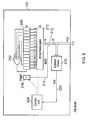
- FIG. 5 A schematic block diagram of the algorithm used to generate the permutation function H(q) is represented in Figure 5 for the 32K mode.
- FIG. 5 An implementation of the address generator 102 for the 32k mode is shown in Figure 5 .
- a linear feed back shift register is formed by thirteen register stages 200 and a xor-gate 202 which is connected to the stages of the shift register 200 in accordance with a generator polynomial. Therefore, in accordance with the content of the shift register 200 a next bit of the shift register is provided from the output of the xor-gate 202 by xoring the content of shift registers R[0], R[1], R[2], R[12] according to the generator polynomial:
- R i ⁇ 13 R i - 1 ⁇ 0 ⁇ R i - 1 ⁇ 1 ⁇ R i - 1 ⁇ 2 ⁇ R i - 1 ⁇ 12
- a pseudo random bit sequence is generated from the content of the shift register 200.
- a permutation circuit 210 is provided which effectively permutes the order of the bits within the shift register 200.1 from an order R' i [n] to an order R i [n ] at the output of the permutation circuit 210.
- Fourteen bits from the output of the permutation circuit 210 are then fed on a connecting channel 212 to which is added a most significant bit via a channel 214 which is provided by a toggle circuit 218.
- a fifteen bit address is therefore generated on channel 212.
- an address check circuit 216 analyses the generated address to determine whether it exceeds a predetermined maximum value.
- the predetermined maximum value may correspond to the maximum number of sub-carrier signals, which are available for data symbols within the COFDM symbol, available for the mode which is being used.
- the interleaver for the 32k mode may also be used for other modes, so that the address generator 102 may also be used for the 2k mode, 4k mode, 8k mode, 16k mode and the 32k mode, by adjusting accordingly the number of the maximum valid address.
- a control signal is generated by the address check unit 216 and fed via a connecting channel 220 to a control unit 224. If the generated address exceeds the predetermined maximum value then this address is rejected and a new address regenerated for the particular symbol.
- R i is derived from R' i by the bit permutations given as follows: Bit permutation for the 32K mode R' i bit positions 13 12 11 10 9 8 7 6 5 4 3 2 1 0 R i bit positions 6 5 0 10 8 1 11 12 2 9 4 3 13 7
- the role of the toggle block is to make sure that we do not generate an address exceeding N max twice in a row. In effect, if an exceeding value was generated, this means that the MSB (i.e. the toggle bit) of the address H(q) was one. So the next value generated will have a MSB set to zero, insuring to produce a valid address.
- the selection of the polynomial generator and the permutation code explained above for the address generator 102 for the 1k mode has been identified following simulation analysis of the relative performance of the interleaver.
- the relative performance of the interleaver has been evaluated using a relative ability of the interleaver to separate successive symbols or an "interleaving quality". As mentioned above, effectively the interleaving must perform for both odd and even symbols, in order to use a single interleaver memory.
- the relative measure of the interleaver quality is determined by defining a distance D (in number of sub-carriers).
- a criterion C is chosen to identify a number of sub-carriers that are at distance ⁇ D at the output of the interleaver that were at distance ⁇ D at the input of the interleaver, the number of sub-carriers for each distance D then being weighted with respect to the relative distance.
- the criterion C is evaluated for both odd and even COFDM symbols. Minimising C produces a superior quality interleaver.
- FIG. 7 provides an example illustration of a receiver which may be used with the present technique.
- a COFDM signal is received by an antenna 300 and detected by a tuner 302 and converted into a digital form by an analogue-to-digital converter 304.
- a guard interval removal processor 306 removes the guard interval from a received COFDM symbol, before the data is recovered from the COFDM symbol using a Fast Fourier Transform (FFT) processor 308 in combination with a channel estimator and correction 310 in co-operation with a embedded-signalling decoding unit 311, in accordance with known techniques.
- FFT Fast Fourier Transform
- the demodulated data is recovered from a mapper 312 and fed to a symbol de-interleaver 314, which operates to effect the reverse mapping of the received data symbol to re-generate an output data stream with the data de-interleaved.
- the symbol de-interleaver 314 is formed from a data processing apparatus as shown in Figure 7 with an interleaver memory 540 and an address generator 542.
- the interleaver memory is as shown in Figure 4 and operates as already explained above to effect de-interleaving by utilising sets of addresses generated by the address generator 542.
- the address generator 542 is formed as shown in Figure 8 and is arranged to generate corresponding addresses to map the data symbols recovered from each COFDM sub-carrier signals into an output data stream.
- the remaining parts of the COFDM receiver shown in Figure 7 are provided to effect error correction decoding 318 to correct errors and recover an estimate of the source data.
- One advantage provided by the present technique for both the receiver and the transmitter is that a symbol interleaver and a symbol de-interleaver operating in the receivers and transmitters can be switched between the 1k, 2k, 4k, 8k, 16k and the 32k mode by changing the generator polynomials and the permutation order.
- the address generator 542 shown in Figure 8 includes an input 544, providing an indication of the mode as well as an input 546 indicating whether there are odd/even COFDM symbols.
- a flexible implementation is thereby provided because a symbol interleaver and de-interleaver can be formed as shown in Figures 3 and 8 , with an address generator as illustrated in either of Figures 5 .
- the address generator can therefore be adapted to the different modes by changing to the generator polynomials and the permutation orders indicated for each of the modes. For example, this can be effected using a software change.
- an embedded signal indicating the mode of the DVB-T2 transmission can be detected in the receiver in the embedded-signalling processing unit 311 and used to configure automatically the symbol de-interleaver in accordance with the detected mode.
- the transmitter and receiver shown in Figures 1 and 7 respectively are provided as illustrations only and are not intended to be limiting.
- the position of the symbol interleaver and the de-interleaver with respect, for example to the bit interleaver and the mapper can be changed.
- the effect of the interleaver and de-interleaver is unchanged by its relative position, although the interleaver may be interleaving I/Q symbols instead of v-bit vectors.
- a corresponding change may be made in the receiver.
- the interleaver and de-interleaver may be operating on different data types, and may be positioned differently to the position described in the example embodiments.
- a data processing apparatus operable to map input symbols to be communicated onto a predetermined number of sub-carrier signals of an Orthogonal Frequency Division Multiplexed (OFDM) symbol.
- the data processing apparatus comprises an interleaver operable to read-into a memory the predetermined number of data symbols for mapping onto the OFDM sub-carrier signals, and to read-out of the memory the data symbols for the OFDM sub-carriers to effect the mapping.
- the read-out is in a different order than the read-in, the order being determined from a set of addresses, with the effect that the data symbols are interleaved on the sub-carrier signals.
- the set of addresses is determined by an address generator, an address being generated for each of the input symbols to indicate one of the sub-carrier signals onto which the data symbol is to be mapped.
- the address generator comprises a linear feedback shift register including a predetermined number of register stages and is operable to generate a pseudo-random bit sequence in accordance with a generator polynomial, and a permutation circuit and a control unit.
- the permutation circuit is operable to receive the content of the shift register stages and to permute the bits present in the register stages in accordance with a permutation order to form an address of one of the OFDM sub-carriers.
- the control unit is operable in combination with an address check circuit to re-generate an address when a generated address exceeds a predetermined maximum valid address.
- embodiments of the present invention find application with DVB standards such as DVB-T, DVB-T2 and DVB-H, which are incorporated herein by reference.
- DVB-H DVB-H standard
- the mobile terminals may be integrated with mobile telephones (whether second, third or higher generation) or Personal Digital Assistants or Tablet PCs for example.
- Such mobile terminals may be capable of receiving DVB-H or DVB-T compatible signals inside buildings or on the move in for example cars or trains, even at high speeds.
- the mobile terminals may be, for example, powered by batteries, mains electricity or low voltage DC supply or powered from a car battery.
- Services that may be provided by DVB-H may include voice, messaging, internet browsing, radio, still and/or moving video images, television services, interactive services, video or near-video on demand and option. The services might operate in combination with one another.
- embodiments of the present invention finds application with the DVB-T2 standard as specified in accordance with ETSI standard EN 302 755.
- embodiments of the present invention find application with the cable transmission standard known as DVB-C2.
- DVB-C2 cable transmission standard
Landscapes
- Engineering & Computer Science (AREA)
- Physics & Mathematics (AREA)
- Probability & Statistics with Applications (AREA)
- Theoretical Computer Science (AREA)
- Signal Processing (AREA)
- Computer Networks & Wireless Communication (AREA)
- Computing Systems (AREA)
- Mathematical Physics (AREA)
- Error Detection And Correction (AREA)
- Detection And Prevention Of Errors In Transmission (AREA)
- Hardware Redundancy (AREA)
- Two-Way Televisions, Distribution Of Moving Picture Or The Like (AREA)
- Communication Control (AREA)
- Circuits Of Receivers In General (AREA)
Priority Applications (1)
| Application Number | Priority Date | Filing Date | Title |
|---|---|---|---|
| PL08253327T PL2056467T3 (pl) | 2007-10-30 | 2008-10-13 | Urządzenie i sposób przetwarzania danych |
Applications Claiming Priority (1)
| Application Number | Priority Date | Filing Date | Title |
|---|---|---|---|
| GB0721272.3A GB2454196B (en) | 2007-10-30 | 2007-10-30 | Data processsing apparatus and method |
Publications (2)
| Publication Number | Publication Date |
|---|---|
| EP2056467A1 true EP2056467A1 (de) | 2009-05-06 |
| EP2056467B1 EP2056467B1 (de) | 2012-02-29 |
Family
ID=38834519
Family Applications (2)
| Application Number | Title | Priority Date | Filing Date |
|---|---|---|---|
| EP08253325A Active EP2056466B1 (de) | 2007-10-30 | 2008-10-13 | Vorrichtung und Verfahren zur Datenverarbeitung |
| EP08253327A Active EP2056467B1 (de) | 2007-10-30 | 2008-10-13 | Vorrichtung und Verfahren zur Datenverarbeitung |
Family Applications Before (1)
| Application Number | Title | Priority Date | Filing Date |
|---|---|---|---|
| EP08253325A Active EP2056466B1 (de) | 2007-10-30 | 2008-10-13 | Vorrichtung und Verfahren zur Datenverarbeitung |
Country Status (16)
| Country | Link |
|---|---|
| US (1) | US8170090B2 (de) |
| EP (2) | EP2056466B1 (de) |
| JP (1) | JP5371374B2 (de) |
| KR (2) | KR101463625B1 (de) |
| CN (1) | CN101425993B (de) |
| AT (2) | ATE547879T1 (de) |
| AU (1) | AU2008230049B2 (de) |
| DK (2) | DK2056467T3 (de) |
| EA (1) | EA014415B1 (de) |
| ES (2) | ES2381053T3 (de) |
| GB (2) | GB2454196B (de) |
| PL (2) | PL2056467T3 (de) |
| PT (2) | PT2056467E (de) |
| TW (2) | TWI451715B (de) |
| UA (1) | UA99256C2 (de) |
| ZA (1) | ZA200808857B (de) |
Families Citing this family (13)
| Publication number | Priority date | Publication date | Assignee | Title |
|---|---|---|---|---|
| GB2454193B (en) | 2007-10-30 | 2012-07-18 | Sony Corp | Data processing apparatus and method |
| US8179954B2 (en) | 2007-10-30 | 2012-05-15 | Sony Corporation | Odd interleaving only of an odd-even interleaver when half or less data subcarriers are active in a digital video broadcasting (DVB) standard |
| TWI427954B (zh) | 2007-10-30 | 2014-02-21 | Sony Corp | 資料處理設備及方法 |
| PL2056464T3 (pl) | 2007-10-30 | 2013-04-30 | Sony Corp | Urządzenie i sposób przetwarzania danych |
| GB2460459B (en) * | 2008-05-30 | 2012-07-11 | Sony Corp | Data processing apparatus and method |
| JP5564853B2 (ja) * | 2009-08-14 | 2014-08-06 | ソニー株式会社 | 受信装置および方法、プログラム、並びに受信システム |
| CN104038453B (zh) * | 2013-03-08 | 2017-04-05 | 清华大学 | 一种抗连续波干扰的通信方法和系统 |
| US9191082B2 (en) | 2013-04-21 | 2015-11-17 | Lg Electronics Inc. | Apparatus for transmitting broadcast signals, apparatus for receiving broadcast signals, method for transmitting broadcast signals and method for receiving broadcast signals |
| JP6346274B2 (ja) | 2013-06-19 | 2018-06-20 | エルジー エレクトロニクス インコーポレイティド | 放送信号送信装置、放送信号受信装置、放送信号送信方法及び放送信号受信方法 |
| KR101477463B1 (ko) * | 2014-09-12 | 2014-12-29 | 김영재 | 칩 운반용 릴테이프 듀얼 와인딩 장치 |
| CN104317525B (zh) * | 2014-09-23 | 2017-08-11 | 天津国芯科技有限公司 | 一种随机存储器的扩展方法及装置 |
| TWI735478B (zh) * | 2015-11-10 | 2021-08-11 | 日商新力股份有限公司 | 資料處理裝置、及資料處理方法 |
| CN113887160B (zh) * | 2021-09-30 | 2022-03-11 | 北京智芯仿真科技有限公司 | 有损耗无频散介质下的集成电路全波电磁仿真方法及系统 |
Citations (3)
| Publication number | Priority date | Publication date | Assignee | Title |
|---|---|---|---|---|
| US6353900B1 (en) | 1998-09-22 | 2002-03-05 | Qualcomm Incorporated | Coding system having state machine based interleaver |
| EP1463255A1 (de) | 2003-03-25 | 2004-09-29 | Sony United Kingdom Limited | Verschachteler zur Symbolabbildung auf den Trägern eines OFDM- (Orthogonale Frequenzmultiplexierung) Systems |
| US20050008084A1 (en) * | 2003-07-09 | 2005-01-13 | Sergey Zhidkov | Apparatus and method for direct measurement of channel state for coded orthogonal frequency division multiplexing receiver |
Family Cites Families (26)
| Publication number | Priority date | Publication date | Assignee | Title |
|---|---|---|---|---|
| US332791A (en) * | 1885-12-22 | Ink-ribbon annunciator for type-writing machines | ||
| US333852A (en) * | 1886-01-05 | Switch and signal apparatus | ||
| US333737A (en) * | 1886-01-05 | Doiee | ||
| US333844A (en) * | 1886-01-05 | Dumping-wagon | ||
| US333116A (en) * | 1885-12-29 | Spring-bed | ||
| US333736A (en) * | 1886-01-05 | Half to asa k | ||
| US33278A (en) * | 1861-09-10 | Improvement in melodeons | ||
| US333588A (en) * | 1886-01-05 | Vehicle-spring | ||
| EP2302808B1 (de) * | 1995-02-01 | 2013-06-05 | Sony Corporation | Mehrkanalübertragung mit Verschachtelung durch in-place Adressierung eines RAM-Speichers |
| EP1239596B8 (de) | 1995-02-01 | 2006-06-28 | Koninklijke Philips Electronics N.V. | Fehlerbeschütztes Datenübertragungs-und Empfangsverfahren und Datenübertragungssystem |
| US6625234B1 (en) * | 1998-12-10 | 2003-09-23 | Nortel Networks Limited | Efficient implementations of proposed turbo code interleavers for third generation code division multiple access |
| US6314534B1 (en) * | 1999-03-31 | 2001-11-06 | Qualcomm Incorporated | Generalized address generation for bit reversed random interleaving |
| US7170849B1 (en) | 2001-03-19 | 2007-01-30 | Cisco Systems Wireless Networking (Australia) Pty Limited | Interleaver, deinterleaver, interleaving method, and deinterleaving method for OFDM data |
| GB0110907D0 (en) | 2001-05-03 | 2001-06-27 | British Broadcasting Corp | Improvements in decoders for many carrier signals, in particular in DVB-T recievers |
| CN100542157C (zh) * | 2002-08-13 | 2009-09-16 | 诺基亚公司 | 符号交织 |
| KR100927144B1 (ko) * | 2002-10-19 | 2009-11-18 | 삼성전자주식회사 | 램덤화 특성이 개선된 내부 인터리버를 가지는 디지털방송시스템의 전송장치 및 그의 전송방법 |
| US8179954B2 (en) * | 2007-10-30 | 2012-05-15 | Sony Corporation | Odd interleaving only of an odd-even interleaver when half or less data subcarriers are active in a digital video broadcasting (DVB) standard |
| GB2454193B (en) * | 2007-10-30 | 2012-07-18 | Sony Corp | Data processing apparatus and method |
| ATE410830T1 (de) * | 2004-03-10 | 2008-10-15 | Ericsson Telefon Ab L M | Addressgenerator für einen verschachtelungsspeicher und einen entschachtelungsspeicher |
| US7395461B2 (en) * | 2005-05-18 | 2008-07-01 | Seagate Technology Llc | Low complexity pseudo-random interleaver |
| US20070115960A1 (en) * | 2005-11-04 | 2007-05-24 | Mediatek Inc. | De-interleaver for data decoding |
| US7688908B2 (en) * | 2007-03-12 | 2010-03-30 | Samsung Electronics Co., Ltd. | System and method for processing wireless high definition video data using a shortened last codeword |
| PL2204002T3 (pl) * | 2007-10-30 | 2013-08-30 | Sony Corp | Urządzenie i sposób przetwarzania danych |
| TWI427954B (zh) * | 2007-10-30 | 2014-02-21 | Sony Corp | 資料處理設備及方法 |
| PL2056464T3 (pl) * | 2007-10-30 | 2013-04-30 | Sony Corp | Urządzenie i sposób przetwarzania danych |
| GB2460459B (en) * | 2008-05-30 | 2012-07-11 | Sony Corp | Data processing apparatus and method |
-
2007
- 2007-10-30 GB GB0721272.3A patent/GB2454196B/en not_active Expired - Fee Related
-
2008
- 2008-10-10 US US12/249,276 patent/US8170090B2/en active Active
- 2008-10-13 DK DK08253327.4T patent/DK2056467T3/da active
- 2008-10-13 ES ES08253327T patent/ES2381053T3/es active Active
- 2008-10-13 PT PT08253327T patent/PT2056467E/pt unknown
- 2008-10-13 EP EP08253325A patent/EP2056466B1/de active Active
- 2008-10-13 GB GB0818760.1A patent/GB2454307B/en not_active Expired - Fee Related
- 2008-10-13 EP EP08253327A patent/EP2056467B1/de active Active
- 2008-10-13 PL PL08253327T patent/PL2056467T3/pl unknown
- 2008-10-13 DK DK08253325.8T patent/DK2056466T3/da active
- 2008-10-13 AT AT08253325T patent/ATE547879T1/de active
- 2008-10-13 PL PL08253325T patent/PL2056466T3/pl unknown
- 2008-10-13 AT AT08253327T patent/ATE547880T1/de active
- 2008-10-13 PT PT08253325T patent/PT2056466E/pt unknown
- 2008-10-13 ES ES08253325T patent/ES2381051T3/es active Active
- 2008-10-14 TW TW097139367A patent/TWI451715B/zh active
- 2008-10-14 TW TW097139368A patent/TWI429247B/zh active
- 2008-10-16 ZA ZA200808857A patent/ZA200808857B/en unknown
- 2008-10-22 AU AU2008230049A patent/AU2008230049B2/en active Active
- 2008-10-29 KR KR1020080106624A patent/KR101463625B1/ko active Active
- 2008-10-29 UA UAA200812693A patent/UA99256C2/ru unknown
- 2008-10-29 JP JP2008278957A patent/JP5371374B2/ja not_active Expired - Fee Related
- 2008-10-29 KR KR1020080106535A patent/KR101463623B1/ko active Active
- 2008-10-29 EA EA200802078A patent/EA014415B1/ru not_active IP Right Cessation
- 2008-10-30 CN CN2008101731085A patent/CN101425993B/zh active Active
Patent Citations (4)
| Publication number | Priority date | Publication date | Assignee | Title |
|---|---|---|---|---|
| US6353900B1 (en) | 1998-09-22 | 2002-03-05 | Qualcomm Incorporated | Coding system having state machine based interleaver |
| EP1463255A1 (de) | 2003-03-25 | 2004-09-29 | Sony United Kingdom Limited | Verschachteler zur Symbolabbildung auf den Trägern eines OFDM- (Orthogonale Frequenzmultiplexierung) Systems |
| EP1463256A1 (de) * | 2003-03-25 | 2004-09-29 | Sony United Kingdom Limited | Verschachteler zur Symbolabbildung auf den Trägern eines OFDM- (Orthogonale Frequenzmultiplexierung) Systems |
| US20050008084A1 (en) * | 2003-07-09 | 2005-01-13 | Sergey Zhidkov | Apparatus and method for direct measurement of channel state for coded orthogonal frequency division multiplexing receiver |
Also Published As
Similar Documents
| Publication | Publication Date | Title |
|---|---|---|
| US10965506B2 (en) | Data processing apparatus and method for use in an interleaver suitable for multiple operating modes | |
| EP2421163B1 (de) | Vorrichtung und Verfahren zur Datenverarbeitung | |
| EP2456077B1 (de) | Vorrichtung und Verfahren zur Datenverarbeitung | |
| EP2056467B1 (de) | Vorrichtung und Verfahren zur Datenverarbeitung | |
| EP2056472B1 (de) | Vorrichtung und Verfahren zur Datenverarbeitung |
Legal Events
| Date | Code | Title | Description |
|---|---|---|---|
| PUAI | Public reference made under article 153(3) epc to a published international application that has entered the european phase |
Free format text: ORIGINAL CODE: 0009012 |
|
| AK | Designated contracting states |
Kind code of ref document: A1 Designated state(s): AT BE BG CH CY CZ DE DK EE ES FI FR GB GR HR HU IE IS IT LI LT LU LV MC MT NL NO PL PT RO SE SI SK TR |
|
| AX | Request for extension of the european patent |
Extension state: AL BA MK RS |
|
| 17P | Request for examination filed |
Effective date: 20091029 |
|
| 17Q | First examination report despatched |
Effective date: 20091119 |
|
| AKX | Designation fees paid |
Designated state(s): AT BE BG CH CY CZ DE DK EE ES FI FR GB GR HR HU IE IS IT LI LT LU LV MC MT NL NO PL PT RO SE SI SK TR |
|
| REG | Reference to a national code |
Ref country code: DE Ref legal event code: R079 Ref document number: 602008013738 Country of ref document: DE Free format text: PREVIOUS MAIN CLASS: H03M0013270000 Ipc: H04L0027260000 |
|
| GRAP | Despatch of communication of intention to grant a patent |
Free format text: ORIGINAL CODE: EPIDOSNIGR1 |
|
| RIC1 | Information provided on ipc code assigned before grant |
Ipc: H04L 1/00 20060101ALI20110908BHEP Ipc: H04L 27/26 20060101AFI20110908BHEP |
|
| RIC1 | Information provided on ipc code assigned before grant |
Ipc: H04L 1/00 20060101ALI20110919BHEP Ipc: H04L 27/26 20060101AFI20110919BHEP |
|
| GRAS | Grant fee paid |
Free format text: ORIGINAL CODE: EPIDOSNIGR3 |
|
| GRAA | (expected) grant |
Free format text: ORIGINAL CODE: 0009210 |
|
| AK | Designated contracting states |
Kind code of ref document: B1 Designated state(s): AT BE BG CH CY CZ DE DK EE ES FI FR GB GR HR HU IE IS IT LI LT LU LV MC MT NL NO PL PT RO SE SI SK TR |
|
| REG | Reference to a national code |
Ref country code: GB Ref legal event code: FG4D Ref country code: CH Ref legal event code: EP |
|
| REG | Reference to a national code |
Ref country code: RO Ref legal event code: EPE |
|
| REG | Reference to a national code |
Ref country code: AT Ref legal event code: REF Ref document number: 547880 Country of ref document: AT Kind code of ref document: T Effective date: 20120315 |
|
| REG | Reference to a national code |
Ref country code: IE Ref legal event code: FG4D |
|
| REG | Reference to a national code |
Ref country code: CH Ref legal event code: NV Representative=s name: MICHELI & CIE SA |
|
| REG | Reference to a national code |
Ref country code: SE Ref legal event code: TRGR |
|
| REG | Reference to a national code |
Ref country code: DE Ref legal event code: R096 Ref document number: 602008013738 Country of ref document: DE Effective date: 20120419 |
|
| REG | Reference to a national code |
Ref country code: PT Ref legal event code: SC4A Free format text: AVAILABILITY OF NATIONAL TRANSLATION Effective date: 20120426 |
|
| REG | Reference to a national code |
Ref country code: DK Ref legal event code: T3 |
|
| REG | Reference to a national code |
Ref country code: ES Ref legal event code: FG2A Ref document number: 2381053 Country of ref document: ES Kind code of ref document: T3 Effective date: 20120522 |
|
| REG | Reference to a national code |
Ref country code: NL Ref legal event code: T3 |
|
| REG | Reference to a national code |
Ref country code: NO Ref legal event code: T2 Effective date: 20120229 |
|
| REG | Reference to a national code |
Ref country code: GR Ref legal event code: EP Ref document number: 20120401039 Country of ref document: GR Effective date: 20120614 |
|
| LTIE | Lt: invalidation of european patent or patent extension |
Effective date: 20120229 |
|
| PG25 | Lapsed in a contracting state [announced via postgrant information from national office to epo] |
Ref country code: LT Free format text: LAPSE BECAUSE OF FAILURE TO SUBMIT A TRANSLATION OF THE DESCRIPTION OR TO PAY THE FEE WITHIN THE PRESCRIBED TIME-LIMIT Effective date: 20120229 Ref country code: IS Free format text: LAPSE BECAUSE OF FAILURE TO SUBMIT A TRANSLATION OF THE DESCRIPTION OR TO PAY THE FEE WITHIN THE PRESCRIBED TIME-LIMIT Effective date: 20120629 Ref country code: HR Free format text: LAPSE BECAUSE OF FAILURE TO SUBMIT A TRANSLATION OF THE DESCRIPTION OR TO PAY THE FEE WITHIN THE PRESCRIBED TIME-LIMIT Effective date: 20120229 |
|
| REG | Reference to a national code |
Ref country code: PL Ref legal event code: T3 |
|
| REG | Reference to a national code |
Ref country code: SK Ref legal event code: T3 Ref document number: E 11767 Country of ref document: SK |
|
| PG25 | Lapsed in a contracting state [announced via postgrant information from national office to epo] |
Ref country code: LV Free format text: LAPSE BECAUSE OF FAILURE TO SUBMIT A TRANSLATION OF THE DESCRIPTION OR TO PAY THE FEE WITHIN THE PRESCRIBED TIME-LIMIT Effective date: 20120229 |
|
| PG25 | Lapsed in a contracting state [announced via postgrant information from national office to epo] |
Ref country code: CY Free format text: LAPSE BECAUSE OF FAILURE TO SUBMIT A TRANSLATION OF THE DESCRIPTION OR TO PAY THE FEE WITHIN THE PRESCRIBED TIME-LIMIT Effective date: 20120229 |
|
| REG | Reference to a national code |
Ref country code: HU Ref legal event code: AG4A Ref document number: E013789 Country of ref document: HU |
|
| PG25 | Lapsed in a contracting state [announced via postgrant information from national office to epo] |
Ref country code: EE Free format text: LAPSE BECAUSE OF FAILURE TO SUBMIT A TRANSLATION OF THE DESCRIPTION OR TO PAY THE FEE WITHIN THE PRESCRIBED TIME-LIMIT Effective date: 20120229 Ref country code: SI Free format text: LAPSE BECAUSE OF FAILURE TO SUBMIT A TRANSLATION OF THE DESCRIPTION OR TO PAY THE FEE WITHIN THE PRESCRIBED TIME-LIMIT Effective date: 20120229 |
|
| PLBE | No opposition filed within time limit |
Free format text: ORIGINAL CODE: 0009261 |
|
| STAA | Information on the status of an ep patent application or granted ep patent |
Free format text: STATUS: NO OPPOSITION FILED WITHIN TIME LIMIT |
|
| 26N | No opposition filed |
Effective date: 20121130 |
|
| REG | Reference to a national code |
Ref country code: DE Ref legal event code: R097 Ref document number: 602008013738 Country of ref document: DE Effective date: 20121130 |
|
| PG25 | Lapsed in a contracting state [announced via postgrant information from national office to epo] |
Ref country code: MC Free format text: LAPSE BECAUSE OF NON-PAYMENT OF DUE FEES Effective date: 20121031 |
|
| PG25 | Lapsed in a contracting state [announced via postgrant information from national office to epo] |
Ref country code: MT Free format text: LAPSE BECAUSE OF FAILURE TO SUBMIT A TRANSLATION OF THE DESCRIPTION OR TO PAY THE FEE WITHIN THE PRESCRIBED TIME-LIMIT Effective date: 20120229 |
|
| PG25 | Lapsed in a contracting state [announced via postgrant information from national office to epo] |
Ref country code: LU Free format text: LAPSE BECAUSE OF NON-PAYMENT OF DUE FEES Effective date: 20121013 |
|
| REG | Reference to a national code |
Ref country code: FR Ref legal event code: PLFP Year of fee payment: 8 |
|
| REG | Reference to a national code |
Ref country code: FR Ref legal event code: PLFP Year of fee payment: 9 |
|
| REG | Reference to a national code |
Ref country code: FR Ref legal event code: PLFP Year of fee payment: 10 |
|
| REG | Reference to a national code |
Ref country code: FR Ref legal event code: PLFP Year of fee payment: 11 |
|
| REG | Reference to a national code |
Ref country code: CH Ref legal event code: NV Representative=s name: DENNEMEYER AG, CH Ref country code: CH Ref legal event code: PUE Owner name: SATURN LICENSING LLC, US Free format text: FORMER OWNER: SONY CORPORATION, JP |
|
| REG | Reference to a national code |
Ref country code: DE Ref legal event code: R082 Ref document number: 602008013738 Country of ref document: DE Representative=s name: DENNEMEYER & ASSOCIATES S.A., LU Ref country code: DE Ref legal event code: R081 Ref document number: 602008013738 Country of ref document: DE Owner name: SATURN LICENSING LLC, NEW YORK, US Free format text: FORMER OWNER: SONY CORPORATION, TOKYO, JP |
|
| REG | Reference to a national code |
Ref country code: NO Ref legal event code: CHAD Owner name: SATURN LICENSING LLC, US Ref country code: NO Ref legal event code: CREP Representative=s name: PLOUGMANN VINGTOFT, POSTBOKS 1003 SENTRUM, 0104 |
|
| REG | Reference to a national code |
Ref country code: NL Ref legal event code: PD Owner name: SATURN LICENSING LLC; US Free format text: DETAILS ASSIGNMENT: CHANGE OF OWNER(S), ASSIGNMENT; FORMER OWNER NAME: SONY CORPORATION Effective date: 20191007 |
|
| REG | Reference to a national code |
Ref country code: ES Ref legal event code: PC2A Owner name: SATURN LICENSING LLC Effective date: 20191028 |
|
| REG | Reference to a national code |
Ref country code: HU Ref legal event code: GB9C Owner name: SATURN LICENSING LLC, US Free format text: FORMER OWNER(S): SONY CORPORATION, JP |
|
| REG | Reference to a national code |
Ref country code: SK Ref legal event code: PC4A Ref document number: E 11767 Country of ref document: SK Owner name: SATURN LICENSING LLC, NEW YORK, NY, US Free format text: FORMER OWNER: SONY CORPORATION, TOKYO, JP Effective date: 20191106 |
|
| REG | Reference to a national code |
Ref country code: BE Ref legal event code: PD Owner name: SATURN LICENSING LLC; US Free format text: DETAILS ASSIGNMENT: CHANGE OF OWNER(S), CESSION; FORMER OWNER NAME: SONY CORPORATION Effective date: 20191015 |
|
| REG | Reference to a national code |
Ref country code: GB Ref legal event code: 732E Free format text: REGISTERED BETWEEN 20200109 AND 20200115 |
|
| REG | Reference to a national code |
Ref country code: AT Ref legal event code: PC Ref document number: 547880 Country of ref document: AT Kind code of ref document: T Owner name: SATURN LICENSING LLC, US Effective date: 20200128 |
|
| PGFP | Annual fee paid to national office [announced via postgrant information from national office to epo] |
Ref country code: CZ Payment date: 20211013 Year of fee payment: 14 Ref country code: FI Payment date: 20211019 Year of fee payment: 14 Ref country code: DK Payment date: 20211022 Year of fee payment: 14 Ref country code: IE Payment date: 20211019 Year of fee payment: 14 |
|
| PGFP | Annual fee paid to national office [announced via postgrant information from national office to epo] |
Ref country code: GR Payment date: 20211022 Year of fee payment: 14 Ref country code: CH Payment date: 20211022 Year of fee payment: 14 Ref country code: BE Payment date: 20211026 Year of fee payment: 14 |
|
| REG | Reference to a national code |
Ref country code: DK Ref legal event code: EBP Effective date: 20221031 |
|
| REG | Reference to a national code |
Ref country code: CH Ref legal event code: PL |
|
| P01 | Opt-out of the competence of the unified patent court (upc) registered |
Effective date: 20230514 |
|
| REG | Reference to a national code |
Ref country code: BE Ref legal event code: MM Effective date: 20221031 |
|
| PG25 | Lapsed in a contracting state [announced via postgrant information from national office to epo] |
Ref country code: LI Free format text: LAPSE BECAUSE OF NON-PAYMENT OF DUE FEES Effective date: 20221031 Ref country code: CZ Free format text: LAPSE BECAUSE OF NON-PAYMENT OF DUE FEES Effective date: 20221013 Ref country code: CH Free format text: LAPSE BECAUSE OF NON-PAYMENT OF DUE FEES Effective date: 20221031 |
|
| PG25 | Lapsed in a contracting state [announced via postgrant information from national office to epo] |
Ref country code: GR Free format text: LAPSE BECAUSE OF NON-PAYMENT OF DUE FEES Effective date: 20230508 |
|
| PG25 | Lapsed in a contracting state [announced via postgrant information from national office to epo] |
Ref country code: BE Free format text: LAPSE BECAUSE OF NON-PAYMENT OF DUE FEES Effective date: 20221031 |
|
| PG25 | Lapsed in a contracting state [announced via postgrant information from national office to epo] |
Ref country code: IE Free format text: LAPSE BECAUSE OF NON-PAYMENT OF DUE FEES Effective date: 20221013 Ref country code: DK Free format text: LAPSE BECAUSE OF NON-PAYMENT OF DUE FEES Effective date: 20221031 |
|
| PG25 | Lapsed in a contracting state [announced via postgrant information from national office to epo] |
Ref country code: FI Free format text: LAPSE BECAUSE OF NON-PAYMENT OF DUE FEES Effective date: 20221013 |
|
| REG | Reference to a national code |
Ref country code: DE Ref legal event code: R082 Ref document number: 602008013738 Country of ref document: DE Representative=s name: DENNEMEYER & ASSOCIATES RECHTSANWALTSGESELLSCH, DE |
|
| PGFP | Annual fee paid to national office [announced via postgrant information from national office to epo] |
Ref country code: PT Payment date: 20250929 Year of fee payment: 18 |
|
| PGFP | Annual fee paid to national office [announced via postgrant information from national office to epo] |
Ref country code: TR Payment date: 20250929 Year of fee payment: 18 Ref country code: PL Payment date: 20250930 Year of fee payment: 18 |
|
| PGFP | Annual fee paid to national office [announced via postgrant information from national office to epo] |
Ref country code: SK Payment date: 20250930 Year of fee payment: 18 |
|
| PGFP | Annual fee paid to national office [announced via postgrant information from national office to epo] |
Ref country code: HU Payment date: 20251013 Year of fee payment: 18 |
|
| PGFP | Annual fee paid to national office [announced via postgrant information from national office to epo] |
Ref country code: NL Payment date: 20251024 Year of fee payment: 18 |
|
| PGFP | Annual fee paid to national office [announced via postgrant information from national office to epo] |
Ref country code: DE Payment date: 20251028 Year of fee payment: 18 |
|
| PGFP | Annual fee paid to national office [announced via postgrant information from national office to epo] |
Ref country code: GB Payment date: 20251023 Year of fee payment: 18 |
|
| PGFP | Annual fee paid to national office [announced via postgrant information from national office to epo] |
Ref country code: NO Payment date: 20251022 Year of fee payment: 18 |
|
| PGFP | Annual fee paid to national office [announced via postgrant information from national office to epo] |
Ref country code: AT Payment date: 20251020 Year of fee payment: 18 |
|
| PGFP | Annual fee paid to national office [announced via postgrant information from national office to epo] |
Ref country code: IT Payment date: 20251022 Year of fee payment: 18 |
|
| PGFP | Annual fee paid to national office [announced via postgrant information from national office to epo] |
Ref country code: FR Payment date: 20251027 Year of fee payment: 18 |
|
| PGFP | Annual fee paid to national office [announced via postgrant information from national office to epo] |
Ref country code: SE Payment date: 20251024 Year of fee payment: 18 |
|
| PGFP | Annual fee paid to national office [announced via postgrant information from national office to epo] |
Ref country code: BG Payment date: 20251028 Year of fee payment: 18 |
|
| PGFP | Annual fee paid to national office [announced via postgrant information from national office to epo] |
Ref country code: RO Payment date: 20251003 Year of fee payment: 18 |
|
| PGFP | Annual fee paid to national office [announced via postgrant information from national office to epo] |
Ref country code: ES Payment date: 20251118 Year of fee payment: 18 |