EP2057746B1 - Drahtloser empfänger und verfahren zum sparen von strom - Google Patents
Drahtloser empfänger und verfahren zum sparen von strom Download PDFInfo
- Publication number
- EP2057746B1 EP2057746B1 EP07789242A EP07789242A EP2057746B1 EP 2057746 B1 EP2057746 B1 EP 2057746B1 EP 07789242 A EP07789242 A EP 07789242A EP 07789242 A EP07789242 A EP 07789242A EP 2057746 B1 EP2057746 B1 EP 2057746B1
- Authority
- EP
- European Patent Office
- Prior art keywords
- receiver
- resolution
- analogue
- mode
- digital converter
- Prior art date
- Legal status (The legal status is an assumption and is not a legal conclusion. Google has not performed a legal analysis and makes no representation as to the accuracy of the status listed.)
- Not-in-force
Links
- 238000000034 method Methods 0.000 title claims description 20
- 238000004891 communication Methods 0.000 claims abstract description 13
- 238000001514 detection method Methods 0.000 claims description 28
- 238000013459 approach Methods 0.000 description 4
- 238000005516 engineering process Methods 0.000 description 4
- 238000010586 diagram Methods 0.000 description 3
- 230000005540 biological transmission Effects 0.000 description 2
- 230000000694 effects Effects 0.000 description 2
- 238000001228 spectrum Methods 0.000 description 2
- 238000013461 design Methods 0.000 description 1
- 238000012986 modification Methods 0.000 description 1
- 230000004048 modification Effects 0.000 description 1
- 230000002093 peripheral effect Effects 0.000 description 1
- 229920001690 polydopamine Polymers 0.000 description 1
- 230000003595 spectral effect Effects 0.000 description 1
Images


Classifications
-
- H—ELECTRICITY
- H03—ELECTRONIC CIRCUITRY
- H03M—CODING; DECODING; CODE CONVERSION IN GENERAL
- H03M1/00—Analogue/digital conversion; Digital/analogue conversion
- H03M1/002—Provisions or arrangements for saving power, e.g. by allowing a sleep mode, using lower supply voltage for downstream stages, using multiple clock domains or by selectively turning on stages when needed
-
- H—ELECTRICITY
- H04—ELECTRIC COMMUNICATION TECHNIQUE
- H04B—TRANSMISSION
- H04B1/00—Details of transmission systems, not covered by a single one of groups H04B3/00 - H04B13/00; Details of transmission systems not characterised by the medium used for transmission
- H04B1/06—Receivers
- H04B1/16—Circuits
- H04B1/1607—Supply circuits
- H04B1/1615—Switching on; Switching off, e.g. remotely
-
- H—ELECTRICITY
- H04—ELECTRIC COMMUNICATION TECHNIQUE
- H04B—TRANSMISSION
- H04B1/00—Details of transmission systems, not covered by a single one of groups H04B3/00 - H04B13/00; Details of transmission systems not characterised by the medium used for transmission
- H04B1/06—Receivers
- H04B1/16—Circuits
-
- H—ELECTRICITY
- H03—ELECTRONIC CIRCUITRY
- H03M—CODING; DECODING; CODE CONVERSION IN GENERAL
- H03M1/00—Analogue/digital conversion; Digital/analogue conversion
- H03M1/12—Analogue/digital converters
-
- H—ELECTRICITY
- H04—ELECTRIC COMMUNICATION TECHNIQUE
- H04W—WIRELESS COMMUNICATION NETWORKS
- H04W52/00—Power management, e.g. Transmission Power Control [TPC] or power classes
- H04W52/02—Power saving arrangements
-
- H—ELECTRICITY
- H04—ELECTRIC COMMUNICATION TECHNIQUE
- H04W—WIRELESS COMMUNICATION NETWORKS
- H04W52/00—Power management, e.g. Transmission Power Control [TPC] or power classes
- H04W52/02—Power saving arrangements
- H04W52/0209—Power saving arrangements in terminal devices
- H04W52/0225—Power saving arrangements in terminal devices using monitoring of external events, e.g. the presence of a signal
-
- Y—GENERAL TAGGING OF NEW TECHNOLOGICAL DEVELOPMENTS; GENERAL TAGGING OF CROSS-SECTIONAL TECHNOLOGIES SPANNING OVER SEVERAL SECTIONS OF THE IPC; TECHNICAL SUBJECTS COVERED BY FORMER USPC CROSS-REFERENCE ART COLLECTIONS [XRACs] AND DIGESTS
- Y02—TECHNOLOGIES OR APPLICATIONS FOR MITIGATION OR ADAPTATION AGAINST CLIMATE CHANGE
- Y02D—CLIMATE CHANGE MITIGATION TECHNOLOGIES IN INFORMATION AND COMMUNICATION TECHNOLOGIES [ICT], I.E. INFORMATION AND COMMUNICATION TECHNOLOGIES AIMING AT THE REDUCTION OF THEIR OWN ENERGY USE
- Y02D30/00—Reducing energy consumption in communication networks
- Y02D30/70—Reducing energy consumption in communication networks in wireless communication networks
Definitions
- the invention relates to a wireless receiver and a method of saving power in a wireless receiver, and in particular to an ultra-wideband (UWB) receiver and method using a power-saving analogue-to-digital converter with switchable resolution.
- UWB ultra-wideband
- Ultra-wideband is a radio technology that transmits digital data across a very wide frequency range, 3.1 to 10.6 GHz. It makes use of ultra low transmission power, typically less than -41 dBm/MHz, so that the technology can literally hide under other transmission frequencies such as existing Wi-Fi, GSM and Bluetooth. This means that ultra-wideband can co-exist with other radio frequency technologies. However, this has the limitation of limiting communication to distances of typically 5 to 20 metres.
- UWB Ultra-wideband
- Figure 1 shows the arrangement of frequency bands in a multi-band orthogonal frequency division multiplexing (MB-OFDM) system for ultra-wideband communication.
- the MB-OFDM system comprises fourteen sub-bands of 528 MHz each, and uses frequency hopping every 312 ns between sub-bands as an access method. Within each sub-band OFDM and QPSK or DCM coding is employed to transmit data. It is noted that the sub-band around 5 GHz, currently 5.1-5.8 GHz, is left blank to avoid interference with existing narrowband systems, for example 802.11a WLAN systems, security agency communication systems, or the aviation industry.
- the fourteen sub-bands are organized into five band groups: four having three 528 MHz sub-bands, and one having two 528 MHz sub-bands.
- the first band group comprises sub-band 1, sub-band 2 and sub-band 3.
- An example UWB system will employ frequency hopping between sub-bands of a band group, such that a first data symbol is transmitted in a first 312.5 ns duration time interval in a first frequency sub-band of a band group, a second data symbol is transmitted in a second 312.5 ns duration time interval in a second frequency sub-band of a band group, and a third data symbol is transmitted in a third 312.5 ns duration time interval in a third frequency sub-band of the band group. Therefore, during each time interval a data symbol is transmitted in a respective sub-band having a bandwidth of 528 MHz, for example sub-band 2 having a 528 MHz baseband signal centred at 3960 MHz
- a superframe consists of 256 medium access slots (MAS), where each MAS has a defined duration, for example 256 ⁇ s.
- MAS medium access slots
- Each superframe starts with a Beacon Period, which lasts one or more contiguous MASs. The start of the first MAS in the beacon period is known as the "beacon period start”.
- ultra-wideband mean that it is being deployed for applications in the field of data communications.
- applications for example, a wide variety of applications exist that focus on cable replacement In the following environments:
- Receivers for MB-OFDM UWB links require a very fast analogue-to-digital converter (ADC) with high resolution.
- a typical ADC for this link will capture a pair of (I,Q) samples at 528 MHz, with a resolution of six bits for each sample.
- the power consumption of the ADC increases with increasing sample rate.
- the power consumption of the ADC also increases exponentially with sample resolution, since the ADC will be a flash converter where power consumption is proportional to the number of comparators, and the number of comparators is proportional to 2 resolution .
- the power consumption of two 528 MHz ADCs with six bits of resolution will therefore be very high.
- WO 00/55977 and WO 01/18970 disclose ADC receivers in which the resolution of an ADC converter is changed according to the quality of a received signal.
- MB-OFDM UWB will be used in portable devices where low power consumption is very important. It is desirable that the UWB receiver within these devices operates continuously, so that it is able to receive frames transmitted by other devices. However, if the UWB receiver operates continuously, this will place an unacceptable load on the power supply, i.e. battery, of a portable device, because the receiver ADC will consume too much power.
- a receiver for receiving a wireless communication signal, the receiver being operable in a first mode when the receiver is actively receiving a transmitted signal, and a second mode when the receiver is waiting to receive a transmitted signal.
- the receiver comprises an analogue to digital converter for converting a received analogue signal into a digital signal; and a receiver controller, adapted to control the operating resolution of the analogue to digital converter such that, in the first mode, the analogue to digital converter operates at a first resolution, and, in the second mode, the analogue to digital converter operates at a second resolution, wherein the second resolution is lower than the first resolution.
- a method of saving power in a receiver having an analogue-to-digital converter for converting a received analogue signal into a digital signal comprises the steps of operating the receiver in a first mode when the receiver is actively receiving a transmitted signal; and operating the receiver in a second mode when the receiver is waiting to receiving a transmitted signal.
- the analogue-to-digital converter has a first resolution when operating in the first mode, and a second resolution when operating in the second mode, the second resolution being lower than the first resolution.
- the invention has the advantage of enabling the average power consumption of a UWB receiver to be reduced by placing the receiver in a low-power "listening" mode when it is not actively receiving a frame.
- the RF and the detection correlator are active, and the ADC is placed in a low-power, low-resolution mode.
- the detection correlator detects the presence of a preamble symbol at the start of a frame, the receiver is powered-up and the ADC placed in a high-resolution mode.
- the receiver may be returned to the "listening" mode.
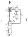
- Figure 2 shows a block schematic diagram of a receiver 10 according to the present invention.
- the receiver 10 comprises an antenna 12 which receives an RF signal 14.
- An RF section 16 amplifies the received signal 14, and outputs the amplified signal 18 to an analogue-to-digital converter 20.
- the receiver 10 further comprises a detection correlator 22, a receiver controller 24, and a receiver baseband 26.
- the receiver 10 has two operating modes: the "receiving" mode (or first mode) in which the receiver operates in a normal mode of operation (i.e. when receiving UWB signals from one or more other UWB devices), and a “listening" mode (or second mode) in which the receiver operates in a power saving mode according to the invention (for example when waiting to receive UWB signals from one or more other UWB devices).
- the "receiving" mode or first mode
- a listening mode or second mode in which the receiver operates in a power saving mode according to the invention (for example when waiting to receive UWB signals from one or more other UWB devices).
- the ADC 20 While operating in the receiving mode, all sections of the receiver 10 are switched on, and the ADC 20 operates at a high resolution, for example a six bit resolution.
- the high-resolution output 38 is sent directly from the ADC 20 to the receiver baseband 26. It will be appreciated that, although the preferred embodiment refers to the high resolution of the ADC 20 being six bits per sample, other resolutions may also be used.
- the receiver controller 24 is adapted to place the receiver 10 in a listening mode to conserve power.
- the receiver 10 can be placed in the listening mode at the end of a frame, or after the last frame of a burst of frames.
- the receiver baseband 26 and all other non-essential sections are placed in a power-save mode, for example switched off, thereby reducing the power consumption of the receiver 10.
- the RF section 16, ADC 20, detection correlator 22 and receiver controller 24 remain switched on, although the power consumption of these blocks may be reduced from normal operation.
- the ADC 20 is configured to operate at a low resolution when the receiver is in the listening mode.
- the low resolution is 1-bit for each sample.
- the power consumption of the ADC 20 is reduced when operating in the 1-bit resolution mode because fewer comparators will be active, thereby further reducing the power consumption of the receiver 10 as a whole.
- the flow diagram of Figure 3 describes the basic principles regarding how the invention controls the operation of the receiver between a normal operating mode, i.e. the receiving mode, and the low power mode, i.e. the listening mode.
- the receiver Upon receiving an indication to enter the listening mode, for example an end of frame signal or after the last frame of a burst of frames, step 301, the receiver is adapted to place the ADC 20 in a low resolution mode of operation, step 303.
- the low resolution mode of operation is a 1-bit mode of operation.
- the receiver While in the listening mode, the receiver is adapted to detect the presence of a preamble signal based on the1-bit output of the ADC 20, step 305. If no preamble is detected, the receiver remains in the listening mode, and the ADC 20 in the 1-bit mode. However, upon detection of a preamble signal, the ADC is set to the high resolution mode once more, step 307.
- the receiver controller 24 receives a "preamble present" signal 32 from the detection correlator 22, the receiver controller 24 will immediately wake up all sections of the receiver 10 and place the ADC 20 into the high-resolution mode, so that the receiver 10 is placed in the "receiving mode", and thus able to receive the incoming frame.
- the receiver controller 24 sends a power-save signal 34 to the receiver baseband 26, instructing the receiver 10 to enter the power-save mode, and sends a resolution-control signal to the ADC 20, instructing the ADC 20 to operate at the lower resolution. Thereafter, the receiver 10 re-enters the listening mode.
- the listening or power-save mode may be achieved, for example, by clock-gating the digital logic within the receiver baseband 26. Clock-gating temporarily disables clocks to registers within inactive digital logic. This significantly reduces the power consumption of the inactive digital logic.
- clock-gating temporarily disables clocks to registers within inactive digital logic. This significantly reduces the power consumption of the inactive digital logic.
- a person skilled in the art will appreciate that many other possible methods for achieving a power-save mode can be provided without departing from the scope of the present invention.
- the invention relies on the detection correlator 22 being able to reliably detect the presence of a preamble symbol in the received signal, and thereafter the receiver 10 being able to switch to receiving mode relatively quickly so that as little information is lost as possible.
- the invention is made possible by the fact that the preamble found in a UWB signal is relatively long.
- the standard MB-OFDM signal includes 24 preamble symbols.
- the 1-bit detection correlator sums how often the sign of the samples in a sliding window (equal to the length of the preamble symbol) coincides with the sign of the expected preamble signal. When this sum is compared to a pre-computed threshold, a reliable decision on the presence or absence of an MB-OFDM preamble can be made.
- the threshold is chosen (by modelling the statistics of the detection correlator) to achieve certain false alarm and missed frame probabilities.
- the above mentioned characteristics of the preamble enable the receiver to be placed in the receiving mode without losing any data.
- the ADC 20 can rapidly switch between high and low resolutions, as this merely involves powering up the necessary extra comparators, for switching to the high resolution, or powering down the unnecessary comparators, for switching to the low resolution.
- the receiver baseband 26 can also switch rapidly between an operational mode and a power-save mode, for example by employing clock-gating as mentioned above.
- the preamble-detection function of the detection correlator 22 could be replaced by an RF power detection circuit.
- Such a circuit would infer the presence of a transmitted signal by detecting radio-frequency power in the received signal. This is a sub-optimal solution, as the RF power detection circuit will not be able to distinguish between preamble symbols and other radio communications.
- such a system would employ the same inventive concept as the present invention, and is therefore to be considered as falling within the scope of the invention as defined in the appended claims.
- the receiver can also be adapted to change the resolution of the ADC during the receiving mode, for example depending on the quality of the signal being received.
- the ADC 20 may be configured to operate at a lower resolution, such as 3-bit, 4-bit or 5-bit, when a high quality signal is being received, and to operate at a 6-bit mode of operation when a poor quality signal is being received.
- the invention may also be used with non-wireless systems where a power saving mode by reducing the accuracy of the ADC is advantageous.
Landscapes
- Engineering & Computer Science (AREA)
- Computer Networks & Wireless Communication (AREA)
- Signal Processing (AREA)
- Theoretical Computer Science (AREA)
- Circuits Of Receivers In General (AREA)
- Mobile Radio Communication Systems (AREA)
- Selective Calling Equipment (AREA)
- Input Circuits Of Receivers And Coupling Of Receivers And Audio Equipment (AREA)
- Superheterodyne Receivers (AREA)
Claims (21)
- Empfänger (10) für den Empfang eines drahtlosen Kommunikationssignals, wobei der Empfänger (10) in einem ersten Arbeitsmodus bedienbar ist, wenn der Empfänger (10) aktiv ein übertragenes Signal empfängt, und in einem zweiten Arbeitsmodus, wenn der Empfänger (10) darauf wartet, ein übertragenes Signal zu empfangen, wobei der Empfänger (10) umfasst
einen Analog-Digital-Umsetzer (20) zum Umsetzen eines empfangenen Analogsignals in ein Digitalsignal; und
eine Empfängersteuerung (24) ausgelegt für die Steuerung der Betriebsauflösung des Analog-Digital-Umsetzers (20), so dass, im ersten Arbeitsmodus, der Analog-Digital-Umsetzer (20) mit einer ersten Auflösung arbeitet und, im zweiten Arbeitsmodus, der Analog-Digital-Umsetzer (20) mit einer zweiten Auflösung arbeitet, wobei die zweite Auflösung niedriger als die erste Auflösung ist. - Empfänger (10) gemäß Anspruch 1, worin die zweite Auflösung des Analog-Digital-Umsetzers (20) eine 1-Bit-Auflösung ist.
- Empfänger (10) gemäß Anspruch 1 oder 2, zudem umfassend
einen Erkennungskorrelator (22) zum Empfang einer Ausgabe vom Analog-Digital-Umsetzer (20);
worin der Erkennungskorrelator (22) ausgelegt ist zum Erkennen des Vorliegens eines Vorsatz-Symbols im digitalisierten Signal auf Basis der zweiten Auflösung des Analog-Digital-Umsetzers (20), wenn der Empfänger (10) im zweiten Arbeitsmodus arbeitet. - Empfänger (10) gemäß Anspruch 3, worin der Erkennungskorrelator (22) ausgelegt ist zum Erkennen des Vorliegens eines Vorsatz-Symbols durch
Summieren, wie oft das Zeichen von Proben in einem Gleitfenster mit dem Zeichen des erwarteten Vorsatz-Symbols übereinstimmt, und
Vergleichen der Summe mit einem vorbestimmten Grenzwert. - Empfänger (10) gemäß Anspruch 4, worin der Erkennungskorrelator (22) zudem ausgelegt ist, ein erstes Steuersignal an die Empfängersteuerung (24) zu senden, welches angibt, dass ein Vorsatz-Symbol vorliegt, wodurch der Analog-Digital-Umsetzer (20) angewiesen wird, mit der ersten Auflösung zu arbeiten.
- Empfänger (10) gemäß Anspruch 1 oder 2, zudem umfassend
eine RF-Stromerkennungsschaltung;
worin die RF-Stromerkennungsschaltung ausgelegt ist, das Vorliegen eines Vorsatz-Symbols auf Basis der Stärke des analogen Signals zu erkennen. - Empfänger (10) gemäß Anspruch 6, worin die RF-Stromerkennungsschaltung zudem ausgelegt ist, ein erstes Steuerungssignal an die Empfängersteuerung (24) zu senden, welches angibt, dass ein Vorsatz-Symbol vorliegt, wodurch der Analog-Digital-Umsetzer (20) angewiesen wird, mit der ersten Auflösung zu arbeiten.
- Empfänger (10) gemäß irgendeinem der vorherigen Ansprüche, worin die erste Auflösung sechs Bit pro Probe ist.
- Empfänger (10) gemäß irgendeinem der vorherigen Ansprüche, worin die Empfängersteuerung (24) zudem ausgelegt ist, die erste Auflösung des Analog-Digital-Umsetzers (20) zu verändern, während der Empfänger im ersten Arbeitsmodus arbeitet.
- Empfänger (10) gemäß irgendeinem der vorherigen Ansprüche, worin zudem umfassend eine Empfänger-Basisbandsektion (26), worin, arbeitet der Empfänger (10) im zweiten Arbeitsmodus, die Empfänger-Basisbandsektion (26) in einen Stromsparmodus gesetzt wird.
- Verfahren zum Stromsparen in einem drahtlosen Empfänger (10) mit einem Analog-Digital-Umsetzer (20) zum Umsetzen eines empfangenen Analogsignals in ein Digitalsignal, wobei das Verfahren die Schritte umfasst
Betreiben des Empfängers (10) in einem ersten Arbeitsmodus, wenn der Empfänger (10) aktiv ein übertragenes Signal empfängt; und
Betreiben des Empfängers (10) in einem zweiten Arbeitsmodus, wenn der Empfänger (10) darauf wartet, ein übertragenes Signal zu empfangen;
worin der Analog-Digital-Umsetzer (20) eine erste Auflösung hat bei Betrieb im ersten Arbeitsmodus und eine zweite Auflösung bei Betrieb im zweiten Arbeitsmodus, wobei die zweite Auflösung niedriger als die erste Auflösung ist. - Verfahren gemäß Anspruch 11, worin die zweite Auflösung des Analog-Digital-Umsetzers (20) bei Betrieb im zweiten Arbeitsmodus auf eine 1-Bit-Auflösung eingestellt wird.
- Verfahren gemäß Anspruch 11 oder 12, zudem umfassend das Bereitstellen eines Erkennungskorrelators (22) zum Empfang einer Ausgabe vom Analog-Digital-Umsetzer (20), wobei der Erkennungskorrelator (22) das Vorliegen eines Vorsatz-Symbols im digitalisierten Signal erkennt, auf Basis der zweiten Auflösung des Analog-Digital-Umsetzers (20), wenn der Empfänger im zweiten Arbeitsmodus arbeitet.
- Verfahren gemäß Anspruch 13, worin das Erkennen des Vorliegens eines Vorsatz-Symbols umfasst die Schritte
Summieren, wie oft das Zeichen von Proben in einem Gleitfenster mit dem Zeichen des erwarteten Vorsatz-Symbols übereinstimmt, und
Vergleichen der Summe mit einem vorbestimmten Grenzwert. - Verfahren gemäß Anspruch 14, zudem umfassend das Anweisen des Analog-Digital-Umsetzers (20), mit der ersten Auflösung zu arbeiten als Reaktion darauf, dass der Erkennungskorrelator (22) das Vorliegen eines Vorsatz-Symbols erkennt.
- Verfahren gemäß Anspruch 11 oder 12, zudem umfassend das Bereitstellen einer RF-Stromerkennungsschaltung zum Erkennen des Vorliegens eines Vorsatz-Symbols auf Basis der Stärke des empfangenen analogen Signals.
- Verfahren gemäß Anspruch 16, zudem umfassend das Anweisen des Analog-Digital-Umsetzers (20), mit der ersten Auflösung zu arbeiten als Reaktion darauf, dass die RF-Stromerkennungsschaltung das Vorliegen eines Vorsatz-Symbols erkennt.
- Verfahren gemäß irgendeinem der Ansprüche 11 bis 17, worin das Betreiben des Analog-Digital-Umsetzers (20) mit der ersten Auflösung das Verwenden einer Auflösung von sechs Bit pro Probe umfasst.
- Verfahren gemäß irgendeinem der Ansprüche 11 bis 18, zudem umfassend das Ändern der ersten Auflösung des Analog-Digital-Umsetzers (20), während der Empfänger (10) im ersten Arbeitsmodus arbeitet.
- Verfahren gemäß irgendeinem der Ansprüche 11 bis 19, zudem umfassend das Bereitstellen einer Empfänger-Basisbandsektion (26) und, arbeitet der Empfänger (10) im zweiten Arbeitsmodus, das Einstellen der Empfänger-Basisbandsektion (26) in einen Stromsparmodus.
- Verfahren gemäß Anspruch 20, worin der Empfängerstrom der Basisbandsektion (26) stufenweise verringert werden kann, um den Stromverbrauch zu optimieren, abhängig von der Empfagssignalqualität des empfangenen Signals.
Applications Claiming Priority (2)
| Application Number | Priority Date | Filing Date | Title |
|---|---|---|---|
| GB0616518A GB2440988A (en) | 2006-08-18 | 2006-08-18 | Wireless receiver with low resolution ADC power saving mode |
| PCT/GB2007/003127 WO2008020216A1 (en) | 2006-08-18 | 2007-08-17 | Wireless receiver and method of saving power |
Publications (2)
| Publication Number | Publication Date |
|---|---|
| EP2057746A1 EP2057746A1 (de) | 2009-05-13 |
| EP2057746B1 true EP2057746B1 (de) | 2011-02-23 |
Family
ID=37081277
Family Applications (1)
| Application Number | Title | Priority Date | Filing Date |
|---|---|---|---|
| EP07789242A Not-in-force EP2057746B1 (de) | 2006-08-18 | 2007-08-17 | Drahtloser empfänger und verfahren zum sparen von strom |
Country Status (12)
| Country | Link |
|---|---|
| US (1) | US20100128817A1 (de) |
| EP (1) | EP2057746B1 (de) |
| JP (1) | JP2010502043A (de) |
| KR (1) | KR20090040913A (de) |
| CN (1) | CN101507124A (de) |
| AT (1) | ATE499751T1 (de) |
| AU (1) | AU2007285552A1 (de) |
| DE (1) | DE602007012720D1 (de) |
| GB (1) | GB2440988A (de) |
| MX (1) | MX2009001614A (de) |
| TW (1) | TW200812309A (de) |
| WO (1) | WO2008020216A1 (de) |
Cited By (1)
| Publication number | Priority date | Publication date | Assignee | Title |
|---|---|---|---|---|
| US9253730B2 (en) | 2012-03-19 | 2016-02-02 | Samsung Electronics Co., Ltd. | Transmitter and receiver for reducing power consumption in FM-UWB communication system |
Families Citing this family (20)
| Publication number | Priority date | Publication date | Assignee | Title |
|---|---|---|---|---|
| US7630331B2 (en) * | 2006-09-27 | 2009-12-08 | Broadcom Corporation | Power control techniques for wireless devices |
| US8073085B1 (en) * | 2007-07-07 | 2011-12-06 | Redpine Signals, Inc. | Analog to digital converter bit width and gain controller for a wireless receiver |
| GB2456647B (en) * | 2008-01-28 | 2012-09-12 | Cambridge Silicon Radio Ltd | Power-savings receiver |
| US8861502B2 (en) | 2008-03-03 | 2014-10-14 | Qualcomm Incorporated | Assisted initial network acquisition and system determination |
| US8798029B2 (en) | 2008-08-06 | 2014-08-05 | Qualcomm Incorporated | Ultra wideband assisted initial acquisition |
| DE102010027019A1 (de) * | 2010-07-08 | 2012-01-12 | Fraunhofer-Gesellschaft zur Förderung der angewandten Forschung e.V. | Empfängeranordnung zum drahtlosen Empfang von Daten |
| US9184756B2 (en) * | 2010-11-08 | 2015-11-10 | Analog Devices, Inc. | Variable dynamic range receiver |
| JP2012191359A (ja) * | 2011-03-09 | 2012-10-04 | Sony Corp | A/d変換装置、a/d変換方法、並びにプログラム |
| US8861414B2 (en) * | 2011-04-08 | 2014-10-14 | The Regents Of The University Of Michigan | Reducing energy consumption in wireless devices |
| US10172105B2 (en) | 2013-07-24 | 2019-01-01 | Silicon Laboratories Inc. | Apparatus for receiver with multi-bit observation interval and associated methods |
| US10305676B2 (en) | 2013-07-24 | 2019-05-28 | Silicon Laboratories Inc. | Apparatus for receiver with digital signal arrival detector and associated methods |
| US9960946B2 (en) * | 2014-07-25 | 2018-05-01 | Samsung Electronics Co., Ltd. | Methods and apparatus for low power operation utilizing multiple ADCs with different precisions |
| US10389482B2 (en) | 2016-12-06 | 2019-08-20 | Silicon Laboratories Inc. | Radio-frequency apparatus with improved power consumption and associated methods |
| EP3556148B1 (de) | 2016-12-14 | 2022-02-02 | Telefonaktiebolaget LM Ericsson (publ) | Aufweck-radio |
| EP3556149B1 (de) | 2016-12-14 | 2021-02-24 | Telefonaktiebolaget LM Ericsson (publ) | Aufweck-signalkonstruktion |
| US20180287832A1 (en) * | 2017-03-29 | 2018-10-04 | Silicon Laboratories Inc. | Radio-Frequency Apparatus with Improved Power Consumption and Associated Methods |
| KR102040396B1 (ko) * | 2018-01-31 | 2019-11-05 | 연세대학교 산학협력단 | 고주파를 이용하는 신호 수신 시스템 및 이 시스템의 수신 신호 처리 방법, 및 이 시스템에 구비되는 해상도 비트 결정 장치 |
| US11095353B2 (en) * | 2019-02-11 | 2021-08-17 | Qualcomm Incorporated | Use of low resolution analog-to-digital converter/digital-to-analog converter |
| CN113078925B (zh) * | 2021-03-17 | 2022-11-01 | 武汉能钠智能装备技术股份有限公司 | 丢帧检测方法、设备、存储介质及装置 |
| US11729838B2 (en) * | 2021-10-07 | 2023-08-15 | Qualcomm Incorporated | Four-step random access channel procedure |
Family Cites Families (8)
| Publication number | Priority date | Publication date | Assignee | Title |
|---|---|---|---|---|
| GB9905997D0 (en) | 1999-03-16 | 1999-05-12 | Koninkl Philips Electronics Nv | Radio receiver |
| JP3428629B2 (ja) * | 1999-03-26 | 2003-07-22 | 日本電気株式会社 | 携帯電話装置及びその電力制御方法 |
| US6504863B1 (en) | 1999-09-07 | 2003-01-07 | Telefonaktiebolaget Lm Ericsson (Publ) | Method and apparatus for adaptive bit resolution in a digital receiver and digital transmitter |
| US6993291B2 (en) * | 2001-10-11 | 2006-01-31 | Nokia Corporation | Method and apparatus for continuously controlling the dynamic range from an analog-to-digital converter |
| JP3647806B2 (ja) * | 2001-12-26 | 2005-05-18 | 松下電器産業株式会社 | A/d変換器、a/d変換方法および信号処理装置 |
| US7522677B2 (en) * | 2003-10-21 | 2009-04-21 | Texas Instruments Incorporated | Receiver with low power listen mode in a wireless local area network |
| US6864817B1 (en) * | 2003-12-30 | 2005-03-08 | Freescale Semiconductor, Inc. | Signaling dependent adaptive analog-to-digital converter (ADC) system and method of using same |
| US7672405B2 (en) * | 2006-05-31 | 2010-03-02 | Via Technologies, Inc. | Method for controlling the signal gain of a multiband orthogonal frequency division multiplexing (MB-OFDM) baseband receiver |
-
2006
- 2006-08-18 GB GB0616518A patent/GB2440988A/en not_active Withdrawn
-
2007
- 2007-08-17 MX MX2009001614A patent/MX2009001614A/es active IP Right Grant
- 2007-08-17 AU AU2007285552A patent/AU2007285552A1/en not_active Abandoned
- 2007-08-17 KR KR1020097005192A patent/KR20090040913A/ko not_active Withdrawn
- 2007-08-17 AT AT07789242T patent/ATE499751T1/de not_active IP Right Cessation
- 2007-08-17 WO PCT/GB2007/003127 patent/WO2008020216A1/en not_active Ceased
- 2007-08-17 EP EP07789242A patent/EP2057746B1/de not_active Not-in-force
- 2007-08-17 JP JP2009524233A patent/JP2010502043A/ja active Pending
- 2007-08-17 DE DE602007012720T patent/DE602007012720D1/de active Active
- 2007-08-17 US US12/377,584 patent/US20100128817A1/en not_active Abandoned
- 2007-08-17 TW TW096130570A patent/TW200812309A/zh unknown
- 2007-08-17 CN CNA2007800306161A patent/CN101507124A/zh active Pending
Cited By (1)
| Publication number | Priority date | Publication date | Assignee | Title |
|---|---|---|---|---|
| US9253730B2 (en) | 2012-03-19 | 2016-02-02 | Samsung Electronics Co., Ltd. | Transmitter and receiver for reducing power consumption in FM-UWB communication system |
Also Published As
| Publication number | Publication date |
|---|---|
| AU2007285552A1 (en) | 2008-02-21 |
| GB0616518D0 (en) | 2006-09-27 |
| ATE499751T1 (de) | 2011-03-15 |
| WO2008020216A1 (en) | 2008-02-21 |
| CN101507124A (zh) | 2009-08-12 |
| US20100128817A1 (en) | 2010-05-27 |
| TW200812309A (en) | 2008-03-01 |
| MX2009001614A (es) | 2009-02-23 |
| GB2440988A (en) | 2008-02-20 |
| JP2010502043A (ja) | 2010-01-21 |
| DE602007012720D1 (de) | 2011-04-07 |
| EP2057746A1 (de) | 2009-05-13 |
| KR20090040913A (ko) | 2009-04-27 |
Similar Documents
| Publication | Publication Date | Title |
|---|---|---|
| US20100128817A1 (en) | Wireless receiver and method of saving power | |
| US6236674B1 (en) | Transceiver control with sleep mode operation | |
| EP3389317B1 (de) | Effizientes präambeldesign und modulationsschemen zum aufwecken von paketen in wlan mit wake-up-funkempfängern | |
| US11917544B2 (en) | Energy-saving signal transmission method and detection method, and device | |
| KR102040828B1 (ko) | 대역폭이 큰 무선랜 시스템에서 저전력 동기화 방법 및 장치 | |
| US11622279B2 (en) | Method for downlink reception in unlicensed band and user equipment using the same | |
| US6760671B1 (en) | Method and apparatus of low power energy detection for a WLAN | |
| EP2557860A1 (de) | Drahtloses Kommunikationsverfahren mit geringem Stromverbrauch | |
| US8477631B2 (en) | Dynamic low power radio modes | |
| JP2013509784A (ja) | 無線通信システムにおけるパワーセービング方法 | |
| TW200644506A (en) | New WLAN TDM protocol | |
| EP2572538B1 (de) | Reduzierung des energieverbrauchs im ruhemodus für überwachung von benachbarten basisstationen | |
| EP2060009B1 (de) | Drahtlose einrichtung und verfahren | |
| KR101574103B1 (ko) | 무선 네트워크에서 채널 액세스를 위한 방법 및 장치 | |
| EP2614596B1 (de) | System und verfahren zur steuerung des stromverbrauchs einer vorrichtung | |
| KR101178248B1 (ko) | 수신 데이터 값들의 결정 | |
| KR20090034432A (ko) | 저전력소비형 임펄스 방식의 송신기, 수신기, 초광대역송수신 시스템 및 그 동작 방법 | |
| US20090092206A1 (en) | Wireless communication apparatus and wireless communication method using plural communication channels having different bandwidths | |
| US20140328233A1 (en) | Portable device for receiving broadcast information | |
| EP4641933A1 (de) | Drahtloser empfänger mit variablem dynamikbereich | |
| JP2006165764A (ja) | 携帯端末装置 | |
| JP2013197865A (ja) | 通信装置 |
Legal Events
| Date | Code | Title | Description |
|---|---|---|---|
| PUAI | Public reference made under article 153(3) epc to a published international application that has entered the european phase |
Free format text: ORIGINAL CODE: 0009012 |
|
| 17P | Request for examination filed |
Effective date: 20090311 |
|
| AK | Designated contracting states |
Kind code of ref document: A1 Designated state(s): AT BE BG CH CY CZ DE DK EE ES FI FR GB GR HU IE IS IT LI LT LU LV MC MT NL PL PT RO SE SI SK TR |
|
| AX | Request for extension of the european patent |
Extension state: AL BA HR MK RS |
|
| 17Q | First examination report despatched |
Effective date: 20090814 |
|
| GRAP | Despatch of communication of intention to grant a patent |
Free format text: ORIGINAL CODE: EPIDOSNIGR1 |
|
| GRAS | Grant fee paid |
Free format text: ORIGINAL CODE: EPIDOSNIGR3 |
|
| DAX | Request for extension of the european patent (deleted) | ||
| GRAA | (expected) grant |
Free format text: ORIGINAL CODE: 0009210 |
|
| AK | Designated contracting states |
Kind code of ref document: B1 Designated state(s): AT BE BG CH CY CZ DE DK EE ES FI FR GB GR HU IE IS IT LI LT LU LV MC MT NL PL PT RO SE SI SK TR |
|
| REG | Reference to a national code |
Ref country code: GB Ref legal event code: FG4D |
|
| REG | Reference to a national code |
Ref country code: CH Ref legal event code: EP |
|
| REG | Reference to a national code |
Ref country code: IE Ref legal event code: FG4D |
|
| REF | Corresponds to: |
Ref document number: 602007012720 Country of ref document: DE Date of ref document: 20110407 Kind code of ref document: P |
|
| REG | Reference to a national code |
Ref country code: DE Ref legal event code: R096 Ref document number: 602007012720 Country of ref document: DE Effective date: 20110407 |
|
| REG | Reference to a national code |
Ref country code: NL Ref legal event code: VDEP Effective date: 20110223 |
|
| LTIE | Lt: invalidation of european patent or patent extension |
Effective date: 20110223 |
|
| PG25 | Lapsed in a contracting state [announced via postgrant information from national office to epo] |
Ref country code: LT Free format text: LAPSE BECAUSE OF FAILURE TO SUBMIT A TRANSLATION OF THE DESCRIPTION OR TO PAY THE FEE WITHIN THE PRESCRIBED TIME-LIMIT Effective date: 20110223 Ref country code: LV Free format text: LAPSE BECAUSE OF FAILURE TO SUBMIT A TRANSLATION OF THE DESCRIPTION OR TO PAY THE FEE WITHIN THE PRESCRIBED TIME-LIMIT Effective date: 20110223 Ref country code: GR Free format text: LAPSE BECAUSE OF FAILURE TO SUBMIT A TRANSLATION OF THE DESCRIPTION OR TO PAY THE FEE WITHIN THE PRESCRIBED TIME-LIMIT Effective date: 20110524 Ref country code: ES Free format text: LAPSE BECAUSE OF FAILURE TO SUBMIT A TRANSLATION OF THE DESCRIPTION OR TO PAY THE FEE WITHIN THE PRESCRIBED TIME-LIMIT Effective date: 20110603 Ref country code: PT Free format text: LAPSE BECAUSE OF FAILURE TO SUBMIT A TRANSLATION OF THE DESCRIPTION OR TO PAY THE FEE WITHIN THE PRESCRIBED TIME-LIMIT Effective date: 20110623 Ref country code: SE Free format text: LAPSE BECAUSE OF FAILURE TO SUBMIT A TRANSLATION OF THE DESCRIPTION OR TO PAY THE FEE WITHIN THE PRESCRIBED TIME-LIMIT Effective date: 20110223 |
|
| PG25 | Lapsed in a contracting state [announced via postgrant information from national office to epo] |
Ref country code: SI Free format text: LAPSE BECAUSE OF FAILURE TO SUBMIT A TRANSLATION OF THE DESCRIPTION OR TO PAY THE FEE WITHIN THE PRESCRIBED TIME-LIMIT Effective date: 20110223 Ref country code: FI Free format text: LAPSE BECAUSE OF FAILURE TO SUBMIT A TRANSLATION OF THE DESCRIPTION OR TO PAY THE FEE WITHIN THE PRESCRIBED TIME-LIMIT Effective date: 20110223 Ref country code: CY Free format text: LAPSE BECAUSE OF FAILURE TO SUBMIT A TRANSLATION OF THE DESCRIPTION OR TO PAY THE FEE WITHIN THE PRESCRIBED TIME-LIMIT Effective date: 20110223 Ref country code: AT Free format text: LAPSE BECAUSE OF FAILURE TO SUBMIT A TRANSLATION OF THE DESCRIPTION OR TO PAY THE FEE WITHIN THE PRESCRIBED TIME-LIMIT Effective date: 20110223 Ref country code: BG Free format text: LAPSE BECAUSE OF FAILURE TO SUBMIT A TRANSLATION OF THE DESCRIPTION OR TO PAY THE FEE WITHIN THE PRESCRIBED TIME-LIMIT Effective date: 20110523 Ref country code: BE Free format text: LAPSE BECAUSE OF FAILURE TO SUBMIT A TRANSLATION OF THE DESCRIPTION OR TO PAY THE FEE WITHIN THE PRESCRIBED TIME-LIMIT Effective date: 20110223 Ref country code: NL Free format text: LAPSE BECAUSE OF FAILURE TO SUBMIT A TRANSLATION OF THE DESCRIPTION OR TO PAY THE FEE WITHIN THE PRESCRIBED TIME-LIMIT Effective date: 20110223 |
|
| PG25 | Lapsed in a contracting state [announced via postgrant information from national office to epo] |
Ref country code: EE Free format text: LAPSE BECAUSE OF FAILURE TO SUBMIT A TRANSLATION OF THE DESCRIPTION OR TO PAY THE FEE WITHIN THE PRESCRIBED TIME-LIMIT Effective date: 20110223 Ref country code: DK Free format text: LAPSE BECAUSE OF FAILURE TO SUBMIT A TRANSLATION OF THE DESCRIPTION OR TO PAY THE FEE WITHIN THE PRESCRIBED TIME-LIMIT Effective date: 20110223 |
|
| PG25 | Lapsed in a contracting state [announced via postgrant information from national office to epo] |
Ref country code: RO Free format text: LAPSE BECAUSE OF FAILURE TO SUBMIT A TRANSLATION OF THE DESCRIPTION OR TO PAY THE FEE WITHIN THE PRESCRIBED TIME-LIMIT Effective date: 20110223 Ref country code: CZ Free format text: LAPSE BECAUSE OF FAILURE TO SUBMIT A TRANSLATION OF THE DESCRIPTION OR TO PAY THE FEE WITHIN THE PRESCRIBED TIME-LIMIT Effective date: 20110223 Ref country code: SK Free format text: LAPSE BECAUSE OF FAILURE TO SUBMIT A TRANSLATION OF THE DESCRIPTION OR TO PAY THE FEE WITHIN THE PRESCRIBED TIME-LIMIT Effective date: 20110223 |
|
| PG25 | Lapsed in a contracting state [announced via postgrant information from national office to epo] |
Ref country code: MT Free format text: LAPSE BECAUSE OF FAILURE TO SUBMIT A TRANSLATION OF THE DESCRIPTION OR TO PAY THE FEE WITHIN THE PRESCRIBED TIME-LIMIT Effective date: 20110223 |
|
| PLBE | No opposition filed within time limit |
Free format text: ORIGINAL CODE: 0009261 |
|
| STAA | Information on the status of an ep patent application or granted ep patent |
Free format text: STATUS: NO OPPOSITION FILED WITHIN TIME LIMIT |
|
| 26N | No opposition filed |
Effective date: 20111124 |
|
| PG25 | Lapsed in a contracting state [announced via postgrant information from national office to epo] |
Ref country code: PL Free format text: LAPSE BECAUSE OF FAILURE TO SUBMIT A TRANSLATION OF THE DESCRIPTION OR TO PAY THE FEE WITHIN THE PRESCRIBED TIME-LIMIT Effective date: 20110223 |
|
| REG | Reference to a national code |
Ref country code: DE Ref legal event code: R097 Ref document number: 602007012720 Country of ref document: DE Effective date: 20111124 |
|
| PG25 | Lapsed in a contracting state [announced via postgrant information from national office to epo] |
Ref country code: MC Free format text: LAPSE BECAUSE OF NON-PAYMENT OF DUE FEES Effective date: 20110831 |
|
| REG | Reference to a national code |
Ref country code: CH Ref legal event code: PL |
|
| GBPC | Gb: european patent ceased through non-payment of renewal fee |
Effective date: 20110817 |
|
| PG25 | Lapsed in a contracting state [announced via postgrant information from national office to epo] |
Ref country code: CH Free format text: LAPSE BECAUSE OF NON-PAYMENT OF DUE FEES Effective date: 20110831 Ref country code: LI Free format text: LAPSE BECAUSE OF NON-PAYMENT OF DUE FEES Effective date: 20110831 |
|
| REG | Reference to a national code |
Ref country code: FR Ref legal event code: ST Effective date: 20120430 |
|
| REG | Reference to a national code |
Ref country code: IE Ref legal event code: MM4A |
|
| PG25 | Lapsed in a contracting state [announced via postgrant information from national office to epo] |
Ref country code: IT Free format text: LAPSE BECAUSE OF FAILURE TO SUBMIT A TRANSLATION OF THE DESCRIPTION OR TO PAY THE FEE WITHIN THE PRESCRIBED TIME-LIMIT Effective date: 20110223 |
|
| REG | Reference to a national code |
Ref country code: DE Ref legal event code: R119 Ref document number: 602007012720 Country of ref document: DE Effective date: 20120301 |
|
| PG25 | Lapsed in a contracting state [announced via postgrant information from national office to epo] |
Ref country code: IE Free format text: LAPSE BECAUSE OF NON-PAYMENT OF DUE FEES Effective date: 20110817 |
|
| PG25 | Lapsed in a contracting state [announced via postgrant information from national office to epo] |
Ref country code: FR Free format text: LAPSE BECAUSE OF NON-PAYMENT OF DUE FEES Effective date: 20110831 Ref country code: GB Free format text: LAPSE BECAUSE OF NON-PAYMENT OF DUE FEES Effective date: 20110817 |
|
| PG25 | Lapsed in a contracting state [announced via postgrant information from national office to epo] |
Ref country code: LU Free format text: LAPSE BECAUSE OF NON-PAYMENT OF DUE FEES Effective date: 20110817 |
|
| PG25 | Lapsed in a contracting state [announced via postgrant information from national office to epo] |
Ref country code: DE Free format text: LAPSE BECAUSE OF NON-PAYMENT OF DUE FEES Effective date: 20120301 |
|
| PG25 | Lapsed in a contracting state [announced via postgrant information from national office to epo] |
Ref country code: IS Free format text: LAPSE BECAUSE OF FAILURE TO SUBMIT A TRANSLATION OF THE DESCRIPTION OR TO PAY THE FEE WITHIN THE PRESCRIBED TIME-LIMIT Effective date: 20110223 |
|
| PG25 | Lapsed in a contracting state [announced via postgrant information from national office to epo] |
Ref country code: TR Free format text: LAPSE BECAUSE OF FAILURE TO SUBMIT A TRANSLATION OF THE DESCRIPTION OR TO PAY THE FEE WITHIN THE PRESCRIBED TIME-LIMIT Effective date: 20110223 |
|
| PG25 | Lapsed in a contracting state [announced via postgrant information from national office to epo] |
Ref country code: HU Free format text: LAPSE BECAUSE OF FAILURE TO SUBMIT A TRANSLATION OF THE DESCRIPTION OR TO PAY THE FEE WITHIN THE PRESCRIBED TIME-LIMIT Effective date: 20110223 |