EP2058075B1 - Verfahren zur Oberflächenbehandlung einer elektrisch leitfähigen Substratoberfläche - Google Patents
Verfahren zur Oberflächenbehandlung einer elektrisch leitfähigen Substratoberfläche Download PDFInfo
- Publication number
- EP2058075B1 EP2058075B1 EP08022415.7A EP08022415A EP2058075B1 EP 2058075 B1 EP2058075 B1 EP 2058075B1 EP 08022415 A EP08022415 A EP 08022415A EP 2058075 B1 EP2058075 B1 EP 2058075B1
- Authority
- EP
- European Patent Office
- Prior art keywords
- tool
- substrate surface
- silicon wafer
- substrate
- anions
- Prior art date
- Legal status (The legal status is an assumption and is not a legal conclusion. Google has not performed a legal analysis and makes no representation as to the accuracy of the status listed.)
- Active
Links
Images
Classifications
-
- B—PERFORMING OPERATIONS; TRANSPORTING
- B23—MACHINE TOOLS; METAL-WORKING NOT OTHERWISE PROVIDED FOR
- B23H—WORKING OF METAL BY THE ACTION OF A HIGH CONCENTRATION OF ELECTRIC CURRENT ON A WORKPIECE USING AN ELECTRODE WHICH TAKES THE PLACE OF A TOOL; SUCH WORKING COMBINED WITH OTHER FORMS OF WORKING OF METAL
- B23H3/00—Electrochemical machining, i.e. removing metal by passing current between an electrode and a workpiece in the presence of an electrolyte
-
- B—PERFORMING OPERATIONS; TRANSPORTING
- B81—MICROSTRUCTURAL TECHNOLOGY
- B81C—PROCESSES OR APPARATUS SPECIALLY ADAPTED FOR THE MANUFACTURE OR TREATMENT OF MICROSTRUCTURAL DEVICES OR SYSTEMS
- B81C1/00—Manufacture or treatment of devices or systems in or on a substrate
- B81C1/00436—Shaping materials, i.e. techniques for structuring the substrate or the layers on the substrate
- B81C1/00634—Processes for shaping materials not provided for in groups B81C1/00444 - B81C1/00626
-
- C—CHEMISTRY; METALLURGY
- C25—ELECTROLYTIC OR ELECTROPHORETIC PROCESSES; APPARATUS THEREFOR
- C25F—PROCESSES FOR THE ELECTROLYTIC REMOVAL OF MATERIALS FROM OBJECTS; APPARATUS THEREFOR
- C25F3/00—Electrolytic etching or polishing
- C25F3/02—Etching
- C25F3/14—Etching locally
-
- B—PERFORMING OPERATIONS; TRANSPORTING
- B81—MICROSTRUCTURAL TECHNOLOGY
- B81C—PROCESSES OR APPARATUS SPECIALLY ADAPTED FOR THE MANUFACTURE OR TREATMENT OF MICROSTRUCTURAL DEVICES OR SYSTEMS
- B81C2201/00—Manufacture or treatment of microstructural devices or systems
- B81C2201/01—Manufacture or treatment of microstructural devices or systems in or on a substrate
- B81C2201/0101—Shaping material; Structuring the bulk substrate or layers on the substrate; Film patterning
- B81C2201/0128—Processes for removing material
- B81C2201/0146—Processes for removing material not provided for in B81C2201/0129 - B81C2201/0145
Definitions
- the invention relates to a method for surface treatment of an electrically conductive substrate surface, with which it is possible to introduce micro- and nanostructures in the surface of the substrate.
- Typical fields of application of such a method are the leveling of technical surfaces for the production of highly planar surfaces, for example in the form of mirror surfaces, or the production of mechanically, electronically and / or optically effective structures.
- Generic methods for surface treatment of substrate surfaces are either known per se material removal methods, such as wet chemical etching techniques, or material deposition methods, such as galvanic methods, sputtering or vapor deposition, to name only a few.
- material deposition methods such as galvanic methods, sputtering or vapor deposition, to name only a few.
- it is necessary to create required process conditions on a substrate surface to be processed for the respective process which are in some cases associated with great expenditure on equipment and thus also with high cost expenditures.
- deposit material layers on a substrate surface it is necessary to have available a corresponding vacuum chamber in which certain material deposits on the substrate surface can be made under vacuum conditions.
- Wet-chemical deposition as well as etching requires the provision of chemical baths with prevailing electrostatic conditions, which in addition to the high procedural complexity also create additional safety and disposal problems.
- planarization techniques for leveling substrate surfaces are known, which are based on chemical mechanical polishing, in particular Cu surfaces in microelectronics.
- reversing by means of the so-called “reverse plating" by reversing a galvanic deposition process supernatant material areas can be removed. This technique can also be used to level material deposits.
- the invention has for its object to provide a surface treatment of electrically conductive substrate surfaces, without having to carry a large apparatus and cost-related effort, it is important to influence the surface texture targeted, i. To structure these in the sense of a local material separation or a local material removal.
- the method according to the invention is intended to be used, in particular, for planarizing substrate surfaces, for example wafers metallized for leveling.
- the method according to the invention for the surface treatment of an electrically conductive substrate surface makes use of a tool having a solid ionic material which is brought into contact, at least in regions, with the electrically conductive substrate surface.
- a silicon wafer surface is provided as the electrically conductive substrate surface.
- the ion conducting Material of the tool is an anionic ion conductor, to which an electrical potential is applied, so that emerge from the anionic ion conductor anions that convert at the silicon wafer surface to a reactive with the silicon wafer surface compound, wherein the reactive compound with the silicon on the silicon wafer surface releases gaseous compound, whereby the silicon wafer surface is removed locally.
- the solution according to the method thus opens depending on the applied between the substrate surface and the tool electrical potential and depending on the choice of material with respect to the substrate or the substrate surface and the respective tool and depending on the shape of the tool, the final shape and size of the contact areas between the tool and the substrate surface determines the possibility of local or entire material erosion on the substrate surface and this without the need to create procedurally complicated process conditions and the necessary apparatus requirements. Rather, the surface treatment according to the invention is based on purely electrochemical processes.
- the tool used to perform the surface treatment of the silicon wafer surface is a solid anionic ionic conductor having a tool surface facing the substrate surface, which is suitably patterned or unstructured depending on the surface treatment target, i. plan or smooth, is formed.
- the tool surface is pressed firmly to the surface treatment on the substrate surface to form an intimate, preferably kraftbeetzschlagten surface contact.
- the tool consisting of an anionic ionic conductor is pressed against the surface of the substrate by force, the tool continuously sinks into the substrate surface as long as the etching process continues, i. as long as the tool is force-pressed against the substrate surface while an electrical potential is applied between the substrate surface and the tool.
- the tool consisting of ion-conducting material is able to transport the metal to be etched completely and without residue, so that the tool does not undergo any change with respect to the chemical composition.
- reaction products occur at the interface between the tool and the substrate surface, possibly also in atomic form, which directly leads to a chemical reaction at the interface between the ion-conductive material tool and the electrically conductive one Guide substrate surface. If such reaction products occur in gaseous form, for example when using fluorine ion conductors, this process can be used for local etching processes.
- pyrex glass as tool material, especially since pyrex glass at temperatures of 300 to 400 ° C represents an ion conductor for alkali ions.
- Another interesting property of Pyrex glass is that it can be bonded to silicon by anodic bonding on the one hand because an electrochemical reaction takes place by means of anodic oxidation in contact with silicon.
- Pyrex glass can absorb ions by diffusion, such as silver ions, which allows the electrical conductivity of Pyrex glass to be adjusted in a targeted manner.
- the method according to the invention can be used for producing optically active structures in the micro and nano range.
- a wafer consisting of pyrex glass is vapor-deposited with a silver layer which subsequently serves as a substrate, on the silver layer of which a second structured pyrex glass wafer serving as a tool is subsequently placed, then by applying an electrical voltage between the substrate and the structured tool, the on the Substrate resting silver layer respectively in the contact areas to the pyrex glass existing tool removed, or completely removed.
- T 400 ° C, electr.
- Voltage 100 V, current flow of 2 mA / cm 2 process time is about 200 sec.
- the replication of three-dimensional silver films on such pyrex glass substrates can also be used to produce so-called gradient index lenses.
- Lenses can be used.
- anionic ion conductors are used as tool materials, such as, for example, CaF 2 , LaF 3 or ZrO 2 , it is possible to reactively etch certain substrate materials on their surface, thereby effectively locally shaping the substrate surface.
- the patterned tool surface of the anionic ion guide tool is placed on the substrate surface, which is the surface of a silicon wafer.
- an electrical potential is applied between the anionic ion conductor of the tool and the silicon wafer, using a fluorine-containing ion conductor, the F - ions from the ion-conductive tool migrate to the silicon wafer surface in contact with the ion conductor Fluorine atoms or fluorine molecules released locally.
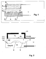
- FIG. 1 represents in which the structured, fluorine-containing surface of the tool 1 is seated on the silicon wafer S, wherein the tool 1 has on the back side an electrolyte 5, which in turn is connected to a cathode K. Due to the potential difference between the tool 1 and the silicon substrate S, fluorine ions migrate to the surface of the tool facing the silicon substrate S 1, at which the fluorine ions are released as reactive gas F 2 and react in the presence of the surface silicon to SiF 4 .
- the ionic conductivity of the ion-conducting tool material and the electrical conductivity of the silicon wafer S can also be increased if the temperature level is increased to temperatures between 200 and 300 ° C. In this way, the reactive etching process on the silicon surface can be significantly improved.
- gaseous reaction products it is also advisable to temporarily remove the tool 1, preferably periodically slightly from the substrate surface and put back on. In this way, the gaseous reaction products can escape laterally. This could for example be accomplished by additional action of ultra or megasonic on the tool.
- a fluoride-containing molten salt as a reservoir of fluorine, which according to embodiment in FIG. 1 is provided in the form of an electrolyte 5.
- an oxygen-conducting material such as zirconium oxide (ZrO 2 )
- materials such as graphite or diamond can be patterned or replicated three-dimensionally, in much the same way as for the structuring of silicon.
- YSZ yttrium stabilized zirconia
- FIG. 2 The simplest construction is in which a suitably shaped tool 1 made of YSZ is placed on the substrate surface 2 made of graphite.
- the ionic conductive ceramic is back with a thin electrically conductive layer 10, in this case of platinum, coat, which nevertheless remains sufficiently permeable to oxygen.
- a voltage U is applied between the graphite and the back of the tool.
- the graphite is still stable to oxygen on the one hand, but on the other hand, the YSZ ceramic of the tool 1 has sufficient conductivity and the graphite is sufficiently reactive to initiate an etching process.
- the oxygen atmosphere O 2 ensures the actual supply of oxygen and prevents the formation of depletion zones in the ion conductor. Under these conditions, it is possible to achieve an etching rate around 12-30 nm / min at a voltage around 80V and a current density around 2 mA / cm 2 . However, a much higher etching rate is achievable. when a higher process temperature is applied. At temperatures above 500 ° C, however, it is absolutely necessary to protect or isolate the graphite from the oxygen.
- the YSZ tool 1 is connected at the back to a ceramic feed line 11, whose inner volume is supplied with an oxygen-containing atmosphere.
- the space outside of this tube is purged with a protective gas, nitrogen or argon. This largely avoids undesirable reaction of the graphite with oxygen radicals.
- a vertical vibrational motion such as ultra or megasonic can be initiated supportive.
Landscapes
- Engineering & Computer Science (AREA)
- Chemical & Material Sciences (AREA)
- Chemical Kinetics & Catalysis (AREA)
- Electrochemistry (AREA)
- Manufacturing & Machinery (AREA)
- Materials Engineering (AREA)
- Metallurgy (AREA)
- Organic Chemistry (AREA)
- Mechanical Engineering (AREA)
- Microelectronics & Electronic Packaging (AREA)
- Weting (AREA)
- Electroplating Methods And Accessories (AREA)
- ing And Chemical Polishing (AREA)
- Diffracting Gratings Or Hologram Optical Elements (AREA)
- Re-Forming, After-Treatment, Cutting And Transporting Of Glass Products (AREA)
- Physical Vapour Deposition (AREA)
- Carbon And Carbon Compounds (AREA)
- Electrodes Of Semiconductors (AREA)
Description
- Die Erfindung bezieht sich auf ein Verfahren zur Oberflächenbehandlung einer elektrisch leitfähigen Substratoberfläche, mit dem es möglich ist Mikro- und Nanostrukturen in die Oberfläche des Substrates einzubringen. Typische Anwendungsbereiche eines derartigen Verfahrens stellen die Einebnung technischer Oberflächen zur Herstellung hochplaner Flächen, bspw. in Form von Spiegeloberflächen, oder die Herstellung mechanisch, elektronisch und/oder optisch wirksamer Strukturen dar.
- Gattungsgemäße Verfahren zur Oberflächenbehandlung von Substratoberflächen, stellen entweder an sich bekannte Materialabtrageverfahren, wie beispielsweise nasschemische Ätztechniken, oder Materialabscheideverfahren dar, wie beispielsweise galvanische Verfahren, Sputter- oder Aufdampfverfahren, um nur einige zu nennen. In allen bekannten Verfahren gilt es an einer zu bearbeitenden Substratoberfläche für den jeweiligen Prozess erforderliche Prozessbedingungen zu schaffen, die zum Teil mit großem apparativen Aufwand und damit auch mit hohen Kostenaufwendungen verbunden sind. Beispielsweise gilt es zur Abscheidung von Materialschichten auf einer Substratoberfläche eine entsprechende Vakuumkammer bereitzuhalten, in der unter Vakuumbedingungen bestimmte Materialabscheidungen an der Substratoberfläche vorgenommen werden können. Der Einsatz nasschemischer Abscheideverfahren sowie auch Ätzverfahren setzt die Bereitstellung chemischer Bäder mit darin vorherrschenden elektrostatischen Bedingungen voraus, die neben dem hohen verfahrenstechnischem Aufwand auch zusätzliche Sicherheits- sowie auch Entsorgungsprobleme entstehen lassen.
- Auch sind Planarisierungstechniken zur Einebnung von Substratoberflächen bekannt, die auf Basis chemisch mechanischen Polierens erfolgen, insbesondere von Cu-Oberflächen in der Mikroelektronik. Daneben können auch mit Hilfe des so genannten "Reverse Plating" durch Umkehrung eines galvanischen Abscheideprozesses überstehende Materialbereiche abgetragen werden. Auch diese Technik kann zur Einebnung von Materialabscheidungen eingesetzt werden.
- Der Erfindung liegt die Aufgabe zugrunde eine Oberflächenbehandlung an elektrisch leitfähigen Substratoberflächen zu ermöglichen, ohne dabei einen großen apparativen sowie auch kostenrelevanten Aufwand tragen zu müssen, wobei es gilt die Oberflächenbeschaffenheit gezielt zu beeinflussen, d.h. diese zu strukturieren im Sinne einer lokalen Materialabscheidung oder auch einer lokalen Materialabtragung. Das lösungsgemäße Verfahren soll insbesondere zur Planarisierung von Substratoberflächen einsetzbar sein, wie beispielsweise zur Einebnung metallisierte Wafer.
- Die der Erfindung zugrunde liegende Aufgabe wird durch ein im Anspruch 1 angegebenen Verfahren gelöst. Den Erfindungsgedanken vorteilhaft weiterbildende Merkmale sind Gegenstand der Unteransprüche sowie der weiteren Beschreibung insbesondere unter Bezugnahme auf die Ausführungsbeispiele zu entnehmen.
- Das lösungsgemäße Verfahren zur Oberflächenbehandlung einer elektrisch leitenden Substratoberfläche bedient sich eines festen Ionen leitenden Materials aufweisenden Werkzeuges, das wenigstens bereichsweise mit der elektrisch leitenden Substratoberfläche in Kontakt gebracht wird. Als elektrisch leitende Substratoberfläche ist eine Siliziumwaferoberfläche vorgesehen. Das Ionen leitende Material des Werkzeuges ist ein anionischer Ionenleiter, an den ein elektrisches Potenzial angelegt wird, so dass aus dem anionischen Ionenleiter Anionen austreten, die sich an der Siliziumwaferoberfläche zu einer mit der Siliziumwaferoberfläche reaktiven Verbindung umwandeln, wobei die reaktionsfähige Verbindung mit dem Silizium an der Siliziumwaferoberfläche eine gasförmige Verbindung freisetzt, wodurch die Siliziumwaferoberfläche lokal abgetragen wird.
- Das lösungsgemäße Verfahren eröffnet somit in Abhängigkeit von dem zwischen der Substratoberfläche und dem Werkzeug angelegten elektrischen Potenzial sowie in Abhängigkeit der Materialwahl hinsichtlich des Substrats bzw. der Substratoberfläche und dem jeweiligen Werkzeug sowie in Abhängigkeit von der Formbeschaffenheit des Werkzeuges, die letztlich Form und Größe der Kontaktbereiche zwischen Werkzeug und Substratoberfläche bestimmt, die Möglichkeit lokale oder ganzflächige Materialabtragungen an der Substratoberfläche vorzunehmen und dies ohne die Notwendigkeit der Schaffung verfahrenstechnisch komplizierter Prozessbedingungen sowie die hierfür erforderlichen apparativen Voraussetzungen. Vielmehr beruht die lösungsgemäße Oberflächenbehandlung auf rein elektrochemische Vorgänge.
- Das Werkzeug, mit dem die lösungsgemäße Oberflächenbehandlung der Siliziumwaferoberfläche durchgeführt wird, besteht aus einem festen anionischen Ionenleiter, der über eine der Substratoberfläche zugewandte Werkzeugoberfläche verfügt, die je nach Oberflächenbehandlungsziel geeignet strukturiert oder unstrukturiert, d.h. plan oder glatt, ausgebildet ist. Die Werkzeugoberfläche wird zur Oberflächenbehandlung fest auf die Substratoberfläche unter Ausbildung eines innigen, vorzugsweise kraftbeaufschlagten Flächenkontaktes angepresst.
- Durch die Emission der Ionen an der Substratoberfläche kommt es analog zu Vorgängen in galvanischen Anlagen mit löslicher Anode zu einem kontinuierlichen Materialabtrag, wobei die Substratoberfläche lokal, d.h. ausschließlich an den Kontaktbereichen zum Werkzeug, geätzt wird.
- Da das aus einem anionischen Ionenleiter bestehende Werkzeug kraftbeaufschlagt gegen die Substratoberfläche gepresst wird, sinkt das Werkzeug kontinuierlich in die Substratoberfläche solange ein, solange der Ätzvorgang andauert, d.h. solange das Werkzeug kraftbeaufschlagt gegen die Substratoberfläche gepresst wird, während ein elektrisches Potenzial zwischen Substratoberfläche und Werkzeug anliegt. Wie bereits erwähnt kommt es im Unterschied zur Verwendung flüssiger Elektrolyte nur zu einem lokalen Ätzvorgang bzw. Materialabtrag im Kontaktbereich, d.h. in jenen Bereichen, in denen das Werkzeug im Flächenkontakt mit der Substratoberfläche steht. Besonders vorteilhaft ist es, wenn das aus Ionen leitende Material bestehende Werkzeug das zu ätzende Metall vollständig und rückstandsfrei zu transportieren vermag, so dass das Werkzeug keine Änderung hinsichtlich der chemischen Zusammensetzung erfährt.
- Durch die Verwendung eines anionischen Ionenleiters als Werkzeugmaterial treten an der Grenzfläche zwischen dem Werkzeug und der Substratoberfläche reaktive Gase auf, gegebenenfalls auch in atomarer Form auf, die unmittelbar zu einer chemischen Reaktion an der Grenzfläche zwischen dem aus Ionen leitenden Material bestehenden Werkzeug und der elektrisch leitenden Substratoberfläche führen. Treten derartige Reaktionsprodukte in gasförmiger Form, beispielsweise bei Verwendung von Fluorionenleitern auf, so kann dieser Prozess für lokale Ätzprozesse genutzt werden.
- Die Erfindung wird nachstehend ohne Beschränkung des allgemeinen Erfindungsgedankens anhand von Ausführungsbeispielen unter Bezugnahme auf die Zeichnungen exemplarisch beschrieben. Es zeigen:
- Fig. 1
- Ausführungsbeispiel zum lokalen Materialabtrag mittels eines anionischen Ionenleiters für Fluorid Ionen sowie
- Fig. 2
- Ausführungsbeispiel zum lokalen Materialabtrag mittels eines anionischen Ionenleiters aus ZrO2.
- Eine Anwendungsmöglichkeit des lösungsgemäßen Verfahrens sieht den Einsatz von Pyrexglas als Werkzeugmaterial vor, zumal Pyrexglas bei Temperaturen von 300 bis 400°C ein lonenleiter für Alkaliionen darstellt. Eine weitere interessante Eigenschaft von Pyrexglas besteht darin, dass es einerseits mit Silizium im Wege des anodischen Bondens verbunden werden kann, da eine elektrochemische Reaktion im Wege einer anodischen Oxidation in Kontakt mit Silizium stattfindet. Andererseits vermag Pyrexglas Ionen im Wege der Diffusion aufzunehmen, wie beispielsweise Silberionen, wodurch die elektrische Leitfähigkeit von Pyrexglas gezielt eingestellt werden kann. Auf der Grundlage dieser Eigenschaften von Pyrexglas kann das lösungsgemäße Verfahren zur Herstellung optisch wirksamer Strukturen im Mikro- und Nanobereich eingesetzt werden. Wird beispielsweise ein aus Pyrexglas bestehender Wafer mit einer Silberschicht bedampft, der nachfolgend als Substrat dient, auf dessen Silberschicht im weiteren ein als Werkzeug dienender zweiter strukturierter Pyrexglaswafer aufgesetzt wird, so kann durch Anlegen einer elektrischen Spannung zwischen dem Substrat und dem strukturierten Werkzeug die auf dem Substrat aufliegende Silberschicht jeweils in den Kontaktbereichen zu dem aus Pyrexglas bestehenden Werkzeug abgetragen, bzw. vollständig entfernt werden. In einem konkret durchgeführten diesbezüglichen Experiment wurden folgende Prozessparamter gewählt: T= 400°C, elektr. Spannung 100 V, Stromfluß 2 mA/cm2, Prozesszeit ca. 200 sec. bei einer Ag-Schichtdicke von ca. 200 nm. Je nach Strukturierung des aus Pyrexglas bestehenden Werkzeuges ist es möglich, auf Waferebene Mikro- und Nanostrukturen herzustellen und entsprechend zu replizieren. Damit eröffnet man sich beispielsweise die Möglichkeit optisch metallische Gitterstrukturen mit Linienbreiten und -abständen von bis hinab zu 20 nm zu replizieren. Derartige Gitterstrukturen können nicht nur als Transmissionsgitter, sondern sogar auch als optische Polarisatoren eingesetzt werden.
- Die Replikation dreidimensionaler Silberfilme auf derartigen Pyrexglassubstraten kann auch dazu eingesetzt werden, um sogenannte Gradientenindex-Linsen herzustellen. Hierzu gilt es zwischen dem mit einer Silberschicht bedampften Pyrexglassubstrat und dem entsprechend strukturierten Pyrexglaswerkzeug eine umgekehrt zum vorstehenden Anwendungsfall gepolte elektrische Spannung anzulegen, so dass das Silber in das Glassubstrat hinein diffundieren kann und somit komplexe Diffusionsprofile innerhalb des Pyrexglassubstrates gebildet werden, die letztlich als Gradientenindex-Linsen eingesetzt werden können.
- Die vorstehend beschriebenen Verfahrensvarianten beschreiben Materialabtragssowie auch Materialabscheideprozesse, bei denen weder Fremdstoffe gebildet werden, noch entsprechende Hilfsstoffe für eine erfolgreiche Prozessdurchführung bereitzustellen sind.
- Werden so genannte anionischen Ionenleiter als Werkzeugmaterialien eingesetzt, wie beispielsweise CaF2, LaF3 oder auch ZrO2, eröffnet sich die Möglichkeit bestimmte Substratmaterialien an ihrer Oberfläche reaktiv zu ätzen und dadurch die Substratoberfläche effektiv lokal abzuformen. Die strukturierte Werkzeugoberfläche des aus anionischen Ionenleitern bestehenden Werkzeuges wird auf der Substratoberfläche aufgesetzt, die die Oberfläche eines Siliziumwafers darstellt. Bei Anlegen eines elektrischen Potenzials zwischen dem anionischen Ionenleiter des Werkzeuges und dem Siliziumwafer wandern bei Verwendung eines Fluor enthaltenen Ionenleiters die F--Ionen aus dem Ionen leitenden Werkzeug an die Silizium-Wafer-Oberfläche, die mit dem Ionenleiter in Kontakt stehen und werden dort als Fluor-Atome bzw. Fluor-Moleküle lokal freigesetzt. Diese, sehr reaktiven Produkte reagieren unmittelbar mit dem Silizium zu SiF4, das gasförmig ist und aus der Grenzfläche zu diffundieren vermag. Diese Situation ist in
Figur 1 dargestellt, bei der die strukturierte, Fluor enthaltene Oberfläche des Werkzeuges 1 auf dem Silizium-Wafer S aufsitzt, wobei das Werkzeug 1 rückseitig einen Elektrolyt 5 aufweist, der wiederum mit einer Kathode K verbunden ist. Durch die zwischen dem Werkzeug 1 und dem Siliziumsubstrat S anliegende Potenzialdifferenz wandern Fluorionen an die dem Siliziumsubstrat S zugewandte Oberfläche des Werkzeuges 1, an der die Fluorionen als reaktives Gas F2 freigesetzt werden und in Gegenwart des oberflächigen Siliziums zu SiF4 reagieren. - Die Ionenleitfähigkeit des Ionen leitenden Werkzeugmaterials sowie die elektrische Leitfähigkeit des Silizium-Wafers S können überdies erhöht werden, sofern das Temperaturniveau auf Temperaturen zwischen 200 und 300°C erhöht wird. Auf diese Weise kann der reaktive Ätzvorgang an der Siliziumoberfläche sehr deutlich verbessert werden.
- Zur Unterstützung des Abtransportes der sich zwischen dem Werkzeug 1 und der Siliziumoberfläche 2 ausbildenden, gasförmigen Reaktionsprodukte bietet es sich ferner an, das Werkzeug 1 zeitweise, vorzugsweise periodisch geringfügig von der Substratoberfläche abzuheben und wieder aufzusetzen. Auf diese Weise können die gasförmigen Reaktionsprodukte seitlich austreten. Dies könnte beispielsweise auch durch zusätzliches Einwirken von Ultra- oder Megaschall auf das Werkzeug bewerkstelligt werden.
- Um sicherzustellen, dass eine Verarmung des Ionen leitenden Werkzeuges 1 an Fluorid-Ionen vermieden wird, gilt es kathodenseitig vorzugsweise eine Fluoridhaltige Salzschmelze als Reservoir an Fluor vorzusehen, die gemäß Ausführungsbeispiel in
Figur 1 in Form eines Elektrolyts 5 bereitgestellt wird. Hiermit eröffnet sich grundsätzlich die Möglichkeit, refraktive oder auch diffraktive Linsen aus Silizium herzustellen bzw. diese zu replizieren. Unter Verwendung eines Sauerstoff leitenden Materials als Werkzeugmaterial, wie beispielsweise Zirkonium-Oxyd (ZrO2) können, ganz analog zur Strukturierung von Silizium, auch Materialien wie Graphit oder Diamant dreidimensional strukturiert bzw. repliziert werden. - Besonders eignet sich als Werkzeugmaterial eine Yttrium stabilisiertes Zirkonoxidkeramik (YSZ). Der einfachste Aufbau ist in
Figur 2 gezeigt, in der ein geeignet ausgeformtes Werkzeug 1 aus YSZ auf die Substratoberfläche 2 aus Graphit aufgesetzt ist. Die Ionenleitfähige Keramik wird rückseitig mit einer dünnen elektrisch leitfähigen Schicht 10, in diesem Fall aus Platin, beschichte, die dennoch hinreichend durchlässig für Sauerstoff bleibt.
Nach Aufsetzten des Werkzeuges 1 auf dem Graphit wird zwischen dem Graphit und der Rückseite des Werkzeuges eine Spannung U angelegt. Um eine ausreichende Ionische Leitfähigkeit der Keramik zu erreichen ist es notwenig die gesamte Anordnung auf eine Temperatur von ca. 400 °C in einer Sauerstoffhaltigen Atmosphäre aufzuheizen. - Unter diesen Bedingungen ist das Graphit gegenüber Sauerstoff einerseits noch stabil, anderseits aber besitzt die YSZ Keramik des Werkzeuges 1 eine ausreichende Leitfähigkeit und das Graphit ist hinreichen reaktiv um einen Ätzprozess in Gang zu bringen. Die Sauerstoffatmosphäre O2 sorgt dabei für den eigentlichen Nachschub an Sauerstoff und verhindert die Ausbildung von Verarmungszonen im Ionenleiter. Unter diesen Bedingungen ist es bei einer Spannung um 80V und einer Stromdichte um 2 mA/cm2 möglich, eine Ätzrate um 12 - 30 nm /min zu erreichen.
Eine deutlich größere Ätzrate ist allerdings erreichbar. wenn eine höhere Prozesstemperatur angewendet wird. Bei Temperaturen oberhalb von 500°C ist es allerdings unbedingt erforderlich das Graphit vor dem Sauerstoff zu schützten bzw. zu isolieren.
In diesem Fall wird das YSZ Werkzeug 1 rückseitig mit einer keramischen Zuleitung 11 verbunden, deren Innenvolumen mit einer Sauerstoffhaltigen Atmosphäre beaufschlagt wird. Der Raum außerhalb dieses Rohrs wird hingegen mit einem Schutzgas, Stickstoff oder Argon, gespült. Damit wird eine unerwünschte Reaktion des Graphits mit Sauerstoffresten weitgehend vermieden. - Um den lateralen Abtransport der Reaktionsprodukte, CO oder CO2, insbesondere bei großflächigen Objekten zu erleichtern, kann unterstützend eine vertikale Vibrationsbewegung wie etwa Ultra- oder Megaschall eingeleitet werden.
- Besonders interessant erscheint dieses Verfahren im Hinblick auf die Herstellung oder Replikation von Presswerkzeugen aus Glaskohlenstoff. Diese Werkzeuge eignen sich insbesondere als Formeneinsätze in Blankpressverfahren von Linsen für sehr hochschmelzende Werkstoffe wie Kieselglas.
-
- 1
- Werkzeug
- 2
- Substratoberfläche
- 3
- konkav-förmige Ausnehmung
- 4
- Umfangsrand
- 5
- Elektrolyt
- S
- Substrat
- A
- Anode
- K
- Kathode
- 10
- Platinschicht
- 11
- Keramische Zuleitung
Claims (11)
- Verfahren zur Oberflächenbehandlung einer elektrisch teilende Substratoberfläche, bei dem ein festes Ionen leitendes Material aufweisendes Werkzeug wenigstens bereichsweise in Kontakt mit der als Siliziumwaferoberfläche ausgebildeten Substratoberfläche gebracht wird, das als anionischer Ionenleiter ausgebildet ist und an das ein elektrisches Potenzial angelegt wird, so dass aus dem anionischen Ionenleiter Anionen austreten, die sich an der Siliziumwaferoberfläche zu einer mit der Siliziumwaferoberfläche reaktiven Verbindung umwandeln, und
dass die reaktionsfähige Verbindung mit dem Silizium an der Siliziumwaferoberfläche eine gasförmige Verbindung freisetzt, wodurch die Siliziumwaferoberfläche lokal abgetragen wird. - Verfahren nach Anspruch 1,
dadurch gekennzeichnet, dass als anionischer Ionenleiter CaF2, LaF3 verwendet wird. - Verfahren nach Anspruch 1 oder 2,
dadurch gekennzeichnet, dass der Abtragsvorgang an der Siliziumwaferoberfläche bei Temperaturen zwischen 200 und 300°C durchgeführt wird. - Verfahren nach einem der Ansprüche 1 bis 3,
dadurch gekennzeichnet, dass als Reservoir an der der Substratoberfläche abgewandten Seite des Werkzeuges ein die Anionen aufnehmender oder abgebender flüssiger Elektrolyt vorgesehen wird. - Verfahren nach einem der Ansprüche 1 bis 4,
dadurch gekennzeichnet, dass das Werkzeug kraftbeaufschlagt auf die Substratoberfläche gepresst wird. - Verfahren nach einem der Ansprüche 1 bis 5,
dadurch gekennzeichnet, dass das Werkzeug eine der Substratoberfläche zugewandte und abgewandte Seite aufweist, und
dass das elektrische Potenzial zwischen der Substratoberfläche und der der Substratoberfläche abgewandte Seite des Werkzeuges angelegt wird. - Verfahren nach einem der Ansprüche 1 bis 6,
dadurch gekennzeichnet, dass bei Verwendung eines Werkzeuges mit einer strukturierten Werkzeugoberfläche, die auf die Substratoberfläche aufgesetzt wird, und durch Anlegen eines elektrischen Potenzials derart, dass Anionen aus der Substratoberfläche in Bereichen, in dienen das Werkzeug mit der Substratoberfläche in Kontakt steht, vom Werkzeug aufgenommen werden, ein lokal begrenzter Materialabtragsvorgang realisiert wird, durch den die Substratoberfläche gleichsam eines lokalen Ätzvorganges strukturiert wird. - Verfahren nach einem der Ansprüche 1 bis 7,
dadurch gekennzeichnet, dass das Anionen leitende Material des Werkzeuges derart ausgewählt wird, dass die von der Substratoberfläche aufgenommenen Anionen ausschließlich durch das Werkzeug transportiert werden ohne dessen chemische Zusammensetzung zu verändern. - Verfahren nach einem der Ansprüche 1 bis 8,
dadurch gekennzeichnet, dass als Reservoir an der der Substratoberfläche abgewandten Seite des Werkzeuges ein die Anionen abgebende gasförmiges Reservoir vorgesehen wird. - Verfahren nach Anspruch 9,
dadurch gekennzeichnet, dass das Reservoir an der der Substratoberfläche abgewandten Seite des Werkzeuges räumlictr von dem Substrat gasdicht getrennt ist. - Verfahren nach einem der Ansprüche 1 bis 10,
dadurch gekennzeichnet, dass das Werkzeug und/oder die Substratoberfläche Vibrationen ausgesetzt wird, so dass die sich zwischen der Werkzeugoberfläche und der Substratoberfläche ausbildende gasförmige Verbindung entweicht.
Applications Claiming Priority (3)
| Application Number | Priority Date | Filing Date | Title |
|---|---|---|---|
| DE102006019189 | 2006-04-21 | ||
| DE102006030323A DE102006030323A1 (de) | 2006-04-21 | 2006-06-30 | Verfahren zur Oberflächenbehandlung einer metallischen Substratoberfläche |
| EP07724433A EP2010351B1 (de) | 2006-04-21 | 2007-04-20 | Verfahren zur oberflächenbehandlung einer elektrisch leitenden, metallischen substratoberfläche |
Related Parent Applications (2)
| Application Number | Title | Priority Date | Filing Date |
|---|---|---|---|
| EP07724433.3 Division | 2007-04-20 | ||
| EP07724433A Division EP2010351B1 (de) | 2006-04-21 | 2007-04-20 | Verfahren zur oberflächenbehandlung einer elektrisch leitenden, metallischen substratoberfläche |
Publications (3)
| Publication Number | Publication Date |
|---|---|
| EP2058075A2 EP2058075A2 (de) | 2009-05-13 |
| EP2058075A3 EP2058075A3 (de) | 2013-02-13 |
| EP2058075B1 true EP2058075B1 (de) | 2014-06-18 |
Family
ID=38536902
Family Applications (3)
| Application Number | Title | Priority Date | Filing Date |
|---|---|---|---|
| EP08022416.5A Active EP2058076B1 (de) | 2006-04-21 | 2007-04-20 | Verfahren zur Oberflächenbehandlung bei der Herstellung eines Presswerkzeuges aus Glaskohlenstoff zum Blankpressen von Linsen. |
| EP07724433A Active EP2010351B1 (de) | 2006-04-21 | 2007-04-20 | Verfahren zur oberflächenbehandlung einer elektrisch leitenden, metallischen substratoberfläche |
| EP08022415.7A Active EP2058075B1 (de) | 2006-04-21 | 2007-04-20 | Verfahren zur Oberflächenbehandlung einer elektrisch leitfähigen Substratoberfläche |
Family Applications Before (2)
| Application Number | Title | Priority Date | Filing Date |
|---|---|---|---|
| EP08022416.5A Active EP2058076B1 (de) | 2006-04-21 | 2007-04-20 | Verfahren zur Oberflächenbehandlung bei der Herstellung eines Presswerkzeuges aus Glaskohlenstoff zum Blankpressen von Linsen. |
| EP07724433A Active EP2010351B1 (de) | 2006-04-21 | 2007-04-20 | Verfahren zur oberflächenbehandlung einer elektrisch leitenden, metallischen substratoberfläche |
Country Status (5)
| Country | Link |
|---|---|
| US (1) | US8758590B2 (de) |
| EP (3) | EP2058076B1 (de) |
| JP (3) | JP5140661B2 (de) |
| DE (1) | DE102006030323A1 (de) |
| WO (1) | WO2007121948A2 (de) |
Families Citing this family (5)
| Publication number | Priority date | Publication date | Assignee | Title |
|---|---|---|---|---|
| DE102009000073A1 (de) | 2009-01-08 | 2010-07-15 | Robert Bosch Gmbh | Verfahren und Vorrichtung zur elektrochemischen Bearbeitung von Substraten |
| KR101613066B1 (ko) * | 2011-12-06 | 2016-04-29 | 고꾸리쯔 다이가꾸 호우징 오사까 다이가꾸 | 고체산화물의 가공방법 |
| US10838297B2 (en) | 2016-09-16 | 2020-11-17 | 3M Innovative Properties Company | Method of making a nanostructured cylindrical roll |
| US12071733B2 (en) | 2022-08-18 | 2024-08-27 | Wirtgen Gmbh | Milling attachment with adjustable cover |
| CN117817059A (zh) * | 2023-12-14 | 2024-04-05 | 南京工业职业技术大学 | 含活性金属成分非晶合金微细电解加工离子扩散控制方法 |
Family Cites Families (18)
| Publication number | Priority date | Publication date | Assignee | Title |
|---|---|---|---|---|
| NL204868A (de) * | 1955-02-25 | |||
| US3653968A (en) | 1970-05-04 | 1972-04-04 | Union Carbide Corp | Solid state electrochemical cells |
| US4155735A (en) * | 1977-11-30 | 1979-05-22 | Ppg Industries, Inc. | Electromigration method for making stained glass photomasks |
| JPS5825488A (ja) | 1981-08-10 | 1983-02-15 | Tatsuya Suzuki | 金の回収装置 |
| JP2515510B2 (ja) * | 1986-08-26 | 1996-07-10 | 株式会社 ケミカル山本 | 鉄鋼材表面に施した亜鉛系被膜の除去方法 |
| US5034023A (en) | 1989-12-21 | 1991-07-23 | Corning Incorporated | Ceramic honeycomb structures as oxygen separators or concentrators |
| DE4242728A1 (de) * | 1992-12-17 | 1994-06-23 | Dornier Gmbh | Keramische Gasanschlußbauteile für Brennstoffzellen mit Zirkonoxid-Festelektrolyt |
| US5403619A (en) | 1993-01-19 | 1995-04-04 | International Business Machines Corporation | Solid state ionic polishing of diamond |
| JP2000232078A (ja) * | 1999-02-10 | 2000-08-22 | Toshiba Corp | メッキ方法及びメッキ装置 |
| DE19960790B4 (de) * | 1999-12-16 | 2006-02-09 | Mtu Aero Engines Gmbh | Elektrode zum elektrochemischen Feinbohren von Werkstücken sowie Verfahren zu ihrer Herstellung |
| WO2002095800A2 (en) | 2001-05-22 | 2002-11-28 | Reflectivity, Inc. | A method for making a micromechanical device by removing a sacrificial layer with multiple sequential etchants |
| DE112004000060B4 (de) * | 2003-07-18 | 2011-01-27 | Nec Corp. | Schaltelemente |
| WO2005042810A2 (en) * | 2003-10-31 | 2005-05-12 | E.I Du Pont De Nemours And Company | Membrane -mediated electropolishing |
| JP2005238420A (ja) * | 2004-02-27 | 2005-09-08 | Rikogaku Shinkokai | 固体中のイオンおよび/または原子の操作方法 |
| DE102004040217A1 (de) * | 2004-08-19 | 2006-03-02 | Mtu Aero Engines Gmbh | Elektrode zum elektrochemischen Senken |
| JP2008539334A (ja) * | 2005-04-29 | 2008-11-13 | イー・アイ・デュポン・ドウ・ヌムール・アンド・カンパニー | 地形状にパターン化された膜を使用した膜介在電解研磨 |
| JP5365829B2 (ja) * | 2005-12-15 | 2013-12-11 | 日本電気株式会社 | スイッチング素子およびその製造方法 |
| US20070215480A1 (en) * | 2006-03-16 | 2007-09-20 | Fang Nicholas X | Pattern transfer by solid state electrochemical stamping |
-
2006
- 2006-06-30 DE DE102006030323A patent/DE102006030323A1/de not_active Ceased
-
2007
- 2007-04-20 US US12/295,321 patent/US8758590B2/en active Active
- 2007-04-20 EP EP08022416.5A patent/EP2058076B1/de active Active
- 2007-04-20 WO PCT/EP2007/003497 patent/WO2007121948A2/de not_active Ceased
- 2007-04-20 JP JP2009505790A patent/JP5140661B2/ja active Active
- 2007-04-20 EP EP07724433A patent/EP2010351B1/de active Active
- 2007-04-20 EP EP08022415.7A patent/EP2058075B1/de active Active
-
2012
- 2012-09-12 JP JP2012200153A patent/JP5484538B2/ja active Active
- 2012-09-12 JP JP2012200152A patent/JP5640055B2/ja active Active
Also Published As
| Publication number | Publication date |
|---|---|
| JP5640055B2 (ja) | 2014-12-10 |
| JP2009534523A (ja) | 2009-09-24 |
| EP2058076B1 (de) | 2014-05-07 |
| JP5484538B2 (ja) | 2014-05-07 |
| EP2010351A2 (de) | 2009-01-07 |
| EP2058076A2 (de) | 2009-05-13 |
| EP2058075A3 (de) | 2013-02-13 |
| EP2058076A3 (de) | 2013-02-13 |
| JP5140661B2 (ja) | 2013-02-06 |
| US20090283416A1 (en) | 2009-11-19 |
| EP2058075A2 (de) | 2009-05-13 |
| EP2010351B1 (de) | 2012-06-27 |
| JP2013032593A (ja) | 2013-02-14 |
| JP2013040406A (ja) | 2013-02-28 |
| WO2007121948A2 (de) | 2007-11-01 |
| WO2007121948A3 (de) | 2008-06-26 |
| DE102006030323A1 (de) | 2007-10-25 |
| US8758590B2 (en) | 2014-06-24 |
Similar Documents
| Publication | Publication Date | Title |
|---|---|---|
| DE69207888T2 (de) | Elektrochemisches Werkzeug zum gleichmässigen Metallabtrag beim Elektropolieren | |
| EP2058075B1 (de) | Verfahren zur Oberflächenbehandlung einer elektrisch leitfähigen Substratoberfläche | |
| US20070224399A1 (en) | Thick porous anodic alumina films and nanowire arrays grown on a solid substrate | |
| WO2015049205A1 (de) | Vorrichtung und verfahren zur kontinuierlichen herstellung poröser siliciumschichten | |
| WO2012104106A1 (de) | Verfahren zum erzeugen einer dreidimensionalen struktur sowie dreidimensionale struktur | |
| EP3796365A2 (de) | Vorrichtung und verfahren zum bonden von substraten | |
| DE102014224587A1 (de) | Verfahren zum Herstellen einer Gassensorvorrichtung zum Erfassen zumindest eines gasförmigen Analyten und Gassensorvorrichtung zum Erfassen zumindest eines gasförmigen Analyten | |
| DE102015106896A1 (de) | Wafer, Verfahren zur Bearbeitung eines Wafers und Verfahren zur Bearbeitung eines Trägers | |
| DE102015117176A1 (de) | Verfahren zum Bearbeiten eines Trägers | |
| DE102014215921A1 (de) | Mikroelektrochemische Sensorvorrichtung | |
| DE102015203307B3 (de) | Verfahren zur Herstellung optisch wirksamer Elemente | |
| DE102020100819A1 (de) | Hermetisch verschlossene transparente Kavität und deren Umhäusung | |
| DE102015117834B4 (de) | Verfahren zur Herstellung einer flexiblen Rod-Array-Anordnung und Rod-Array-Anordnung | |
| EP3983575A1 (de) | Elektrolysevorrichtung mit zwei bor dotierten diamantschichten | |
| DE10340750A1 (de) | Trockenätzvorrichtung und Trockenätzverfahren sowie in Trockenätzvorrichtung verwendetes Reinigungsverfahren | |
| DE102015117833B4 (de) | Verfahren zur Herstellung einer feldförmigen, homogenen Rod-Anordnung und deren Verwendung | |
| EP4213974B1 (de) | Hierarchisch poröse struktur und prozess zur herstellung derselbigen | |
| DE102016112125B4 (de) | Verfahren zur Herstellung eines Festelektrolyts | |
| RU2562619C1 (ru) | Способ получения структурированных сплошных и островковых пленок на поверхности стекла | |
| DE102019112472B3 (de) | Verfahren zur Herstellung eines ein Trägersubstrat aufweisenden Displays sowie ein nach diesem Verfahren hergestelltes Trägersubstrat | |
| EP3580786A2 (de) | Verfahren zum texturieren einer oberfläche eines halbleitermaterials sowie vorrichtung zur durchführung des verfahrens | |
| EP4347929A1 (de) | Verfahren zur herstellung hochgenau lokalisierter breitbandabsorber für 2d- und 3d-oberflächen | |
| DE102020201567A1 (de) | Herstellungsverfahren für ein mikromechanisches Bauelement und entsprechendes mikromechanisches Bauelement | |
| Abdolvand et al. | Silver-doped nanocomposite glass as a base material for fine metallodielectric microstructuring | |
| EP0245764A1 (de) | Mit Silicium elektrisch leitfähig und oxidationsbeständig beschichtete Graphit-Elektrode und Verfahren zu ihrer Herstellung |
Legal Events
| Date | Code | Title | Description |
|---|---|---|---|
| PUAI | Public reference made under article 153(3) epc to a published international application that has entered the european phase |
Free format text: ORIGINAL CODE: 0009012 |
|
| 17P | Request for examination filed |
Effective date: 20081223 |
|
| AC | Divisional application: reference to earlier application |
Ref document number: 2010351 Country of ref document: EP Kind code of ref document: P |
|
| AK | Designated contracting states |
Kind code of ref document: A2 Designated state(s): AT BE BG CH CY CZ DE DK EE ES FI FR GB GR HU IE IS IT LI LT LU LV MC MT NL PL PT RO SE SI SK TR |
|
| AX | Request for extension of the european patent |
Extension state: AL BA HR MK RS |
|
| RIC1 | Information provided on ipc code assigned before grant |
Ipc: B23H 3/00 20060101AFI20121113BHEP Ipc: C25D 3/00 20060101ALI20121113BHEP |
|
| PUAL | Search report despatched |
Free format text: ORIGINAL CODE: 0009013 |
|
| AK | Designated contracting states |
Kind code of ref document: A3 Designated state(s): AT BE BG CH CY CZ DE DK EE ES FI FR GB GR HU IE IS IT LI LT LU LV MC MT NL PL PT RO SE SI SK TR |
|
| AX | Request for extension of the european patent |
Extension state: AL BA HR MK RS |
|
| RIC1 | Information provided on ipc code assigned before grant |
Ipc: C25D 3/00 20060101ALI20130109BHEP Ipc: B23H 3/00 20060101AFI20130109BHEP |
|
| AKX | Designation fees paid |
Designated state(s): AT BE BG CH CY CZ DE DK EE ES FI FR GB GR HU IE IS IT LI LT LU LV MC MT NL PL PT RO SE SI SK TR |
|
| GRAP | Despatch of communication of intention to grant a patent |
Free format text: ORIGINAL CODE: EPIDOSNIGR1 |
|
| INTG | Intention to grant announced |
Effective date: 20131216 |
|
| GRAS | Grant fee paid |
Free format text: ORIGINAL CODE: EPIDOSNIGR3 |
|
| GRAA | (expected) grant |
Free format text: ORIGINAL CODE: 0009210 |
|
| AC | Divisional application: reference to earlier application |
Ref document number: 2010351 Country of ref document: EP Kind code of ref document: P |
|
| AK | Designated contracting states |
Kind code of ref document: B1 Designated state(s): AT BE BG CH CY CZ DE DK EE ES FI FR GB GR HU IE IS IT LI LT LU LV MC MT NL PL PT RO SE SI SK TR |
|
| REG | Reference to a national code |
Ref country code: GB Ref legal event code: FG4D Free format text: NOT ENGLISH |
|
| REG | Reference to a national code |
Ref country code: CH Ref legal event code: EP |
|
| REG | Reference to a national code |
Ref country code: AT Ref legal event code: REF Ref document number: 673049 Country of ref document: AT Kind code of ref document: T Effective date: 20140715 |
|
| REG | Reference to a national code |
Ref country code: IE Ref legal event code: FG4D Free format text: LANGUAGE OF EP DOCUMENT: GERMAN |
|
| REG | Reference to a national code |
Ref country code: DE Ref legal event code: R096 Ref document number: 502007013214 Country of ref document: DE Effective date: 20140731 |
|
| PG25 | Lapsed in a contracting state [announced via postgrant information from national office to epo] |
Ref country code: CY Free format text: LAPSE BECAUSE OF FAILURE TO SUBMIT A TRANSLATION OF THE DESCRIPTION OR TO PAY THE FEE WITHIN THE PRESCRIBED TIME-LIMIT Effective date: 20140618 Ref country code: GR Free format text: LAPSE BECAUSE OF FAILURE TO SUBMIT A TRANSLATION OF THE DESCRIPTION OR TO PAY THE FEE WITHIN THE PRESCRIBED TIME-LIMIT Effective date: 20140919 Ref country code: LT Free format text: LAPSE BECAUSE OF FAILURE TO SUBMIT A TRANSLATION OF THE DESCRIPTION OR TO PAY THE FEE WITHIN THE PRESCRIBED TIME-LIMIT Effective date: 20140618 Ref country code: FI Free format text: LAPSE BECAUSE OF FAILURE TO SUBMIT A TRANSLATION OF THE DESCRIPTION OR TO PAY THE FEE WITHIN THE PRESCRIBED TIME-LIMIT Effective date: 20140618 |
|
| REG | Reference to a national code |
Ref country code: NL Ref legal event code: VDEP Effective date: 20140618 |
|
| REG | Reference to a national code |
Ref country code: LT Ref legal event code: MG4D |
|
| PG25 | Lapsed in a contracting state [announced via postgrant information from national office to epo] |
Ref country code: LV Free format text: LAPSE BECAUSE OF FAILURE TO SUBMIT A TRANSLATION OF THE DESCRIPTION OR TO PAY THE FEE WITHIN THE PRESCRIBED TIME-LIMIT Effective date: 20140618 Ref country code: SE Free format text: LAPSE BECAUSE OF FAILURE TO SUBMIT A TRANSLATION OF THE DESCRIPTION OR TO PAY THE FEE WITHIN THE PRESCRIBED TIME-LIMIT Effective date: 20140618 |
|
| PG25 | Lapsed in a contracting state [announced via postgrant information from national office to epo] |
Ref country code: SK Free format text: LAPSE BECAUSE OF FAILURE TO SUBMIT A TRANSLATION OF THE DESCRIPTION OR TO PAY THE FEE WITHIN THE PRESCRIBED TIME-LIMIT Effective date: 20140618 Ref country code: PT Free format text: LAPSE BECAUSE OF FAILURE TO SUBMIT A TRANSLATION OF THE DESCRIPTION OR TO PAY THE FEE WITHIN THE PRESCRIBED TIME-LIMIT Effective date: 20141020 Ref country code: CZ Free format text: LAPSE BECAUSE OF FAILURE TO SUBMIT A TRANSLATION OF THE DESCRIPTION OR TO PAY THE FEE WITHIN THE PRESCRIBED TIME-LIMIT Effective date: 20140618 Ref country code: RO Free format text: LAPSE BECAUSE OF FAILURE TO SUBMIT A TRANSLATION OF THE DESCRIPTION OR TO PAY THE FEE WITHIN THE PRESCRIBED TIME-LIMIT Effective date: 20140618 Ref country code: EE Free format text: LAPSE BECAUSE OF FAILURE TO SUBMIT A TRANSLATION OF THE DESCRIPTION OR TO PAY THE FEE WITHIN THE PRESCRIBED TIME-LIMIT Effective date: 20140618 Ref country code: ES Free format text: LAPSE BECAUSE OF FAILURE TO SUBMIT A TRANSLATION OF THE DESCRIPTION OR TO PAY THE FEE WITHIN THE PRESCRIBED TIME-LIMIT Effective date: 20140618 |
|
| PG25 | Lapsed in a contracting state [announced via postgrant information from national office to epo] |
Ref country code: PL Free format text: LAPSE BECAUSE OF FAILURE TO SUBMIT A TRANSLATION OF THE DESCRIPTION OR TO PAY THE FEE WITHIN THE PRESCRIBED TIME-LIMIT Effective date: 20140618 Ref country code: IS Free format text: LAPSE BECAUSE OF FAILURE TO SUBMIT A TRANSLATION OF THE DESCRIPTION OR TO PAY THE FEE WITHIN THE PRESCRIBED TIME-LIMIT Effective date: 20141018 Ref country code: NL Free format text: LAPSE BECAUSE OF FAILURE TO SUBMIT A TRANSLATION OF THE DESCRIPTION OR TO PAY THE FEE WITHIN THE PRESCRIBED TIME-LIMIT Effective date: 20140618 |
|
| REG | Reference to a national code |
Ref country code: DE Ref legal event code: R097 Ref document number: 502007013214 Country of ref document: DE |
|
| PLBE | No opposition filed within time limit |
Free format text: ORIGINAL CODE: 0009261 |
|
| STAA | Information on the status of an ep patent application or granted ep patent |
Free format text: STATUS: NO OPPOSITION FILED WITHIN TIME LIMIT |
|
| PG25 | Lapsed in a contracting state [announced via postgrant information from national office to epo] |
Ref country code: DK Free format text: LAPSE BECAUSE OF FAILURE TO SUBMIT A TRANSLATION OF THE DESCRIPTION OR TO PAY THE FEE WITHIN THE PRESCRIBED TIME-LIMIT Effective date: 20140618 Ref country code: IT Free format text: LAPSE BECAUSE OF FAILURE TO SUBMIT A TRANSLATION OF THE DESCRIPTION OR TO PAY THE FEE WITHIN THE PRESCRIBED TIME-LIMIT Effective date: 20140618 |
|
| 26N | No opposition filed |
Effective date: 20150319 |
|
| PG25 | Lapsed in a contracting state [announced via postgrant information from national office to epo] |
Ref country code: SI Free format text: LAPSE BECAUSE OF FAILURE TO SUBMIT A TRANSLATION OF THE DESCRIPTION OR TO PAY THE FEE WITHIN THE PRESCRIBED TIME-LIMIT Effective date: 20140618 |
|
| PG25 | Lapsed in a contracting state [announced via postgrant information from national office to epo] |
Ref country code: LU Free format text: LAPSE BECAUSE OF FAILURE TO SUBMIT A TRANSLATION OF THE DESCRIPTION OR TO PAY THE FEE WITHIN THE PRESCRIBED TIME-LIMIT Effective date: 20150420 Ref country code: MC Free format text: LAPSE BECAUSE OF FAILURE TO SUBMIT A TRANSLATION OF THE DESCRIPTION OR TO PAY THE FEE WITHIN THE PRESCRIBED TIME-LIMIT Effective date: 20140618 |
|
| REG | Reference to a national code |
Ref country code: CH Ref legal event code: PL |
|
| REG | Reference to a national code |
Ref country code: IE Ref legal event code: MM4A |
|
| PG25 | Lapsed in a contracting state [announced via postgrant information from national office to epo] |
Ref country code: LI Free format text: LAPSE BECAUSE OF NON-PAYMENT OF DUE FEES Effective date: 20150430 Ref country code: CH Free format text: LAPSE BECAUSE OF NON-PAYMENT OF DUE FEES Effective date: 20150430 |
|
| REG | Reference to a national code |
Ref country code: FR Ref legal event code: PLFP Year of fee payment: 10 |
|
| PG25 | Lapsed in a contracting state [announced via postgrant information from national office to epo] |
Ref country code: IE Free format text: LAPSE BECAUSE OF NON-PAYMENT OF DUE FEES Effective date: 20150420 |
|
| REG | Reference to a national code |
Ref country code: AT Ref legal event code: MM01 Ref document number: 673049 Country of ref document: AT Kind code of ref document: T Effective date: 20150420 |
|
| PG25 | Lapsed in a contracting state [announced via postgrant information from national office to epo] |
Ref country code: AT Free format text: LAPSE BECAUSE OF NON-PAYMENT OF DUE FEES Effective date: 20150420 |
|
| PG25 | Lapsed in a contracting state [announced via postgrant information from national office to epo] |
Ref country code: MT Free format text: LAPSE BECAUSE OF FAILURE TO SUBMIT A TRANSLATION OF THE DESCRIPTION OR TO PAY THE FEE WITHIN THE PRESCRIBED TIME-LIMIT Effective date: 20140618 |
|
| REG | Reference to a national code |
Ref country code: FR Ref legal event code: PLFP Year of fee payment: 11 |
|
| PG25 | Lapsed in a contracting state [announced via postgrant information from national office to epo] |
Ref country code: HU Free format text: LAPSE BECAUSE OF FAILURE TO SUBMIT A TRANSLATION OF THE DESCRIPTION OR TO PAY THE FEE WITHIN THE PRESCRIBED TIME-LIMIT; INVALID AB INITIO Effective date: 20070420 Ref country code: BG Free format text: LAPSE BECAUSE OF FAILURE TO SUBMIT A TRANSLATION OF THE DESCRIPTION OR TO PAY THE FEE WITHIN THE PRESCRIBED TIME-LIMIT Effective date: 20140618 |
|
| PG25 | Lapsed in a contracting state [announced via postgrant information from national office to epo] |
Ref country code: BE Free format text: LAPSE BECAUSE OF NON-PAYMENT OF DUE FEES Effective date: 20150430 |
|
| PG25 | Lapsed in a contracting state [announced via postgrant information from national office to epo] |
Ref country code: TR Free format text: LAPSE BECAUSE OF FAILURE TO SUBMIT A TRANSLATION OF THE DESCRIPTION OR TO PAY THE FEE WITHIN THE PRESCRIBED TIME-LIMIT Effective date: 20140618 |
|
| REG | Reference to a national code |
Ref country code: FR Ref legal event code: PLFP Year of fee payment: 12 |
|
| P01 | Opt-out of the competence of the unified patent court (upc) registered |
Effective date: 20230524 |
|
| PGFP | Annual fee paid to national office [announced via postgrant information from national office to epo] |
Ref country code: DE Payment date: 20250417 Year of fee payment: 19 |
|
| PGFP | Annual fee paid to national office [announced via postgrant information from national office to epo] |
Ref country code: FR Payment date: 20250422 Year of fee payment: 19 |
|
| PGFP | Annual fee paid to national office [announced via postgrant information from national office to epo] |
Ref country code: GB Payment date: 20260324 Year of fee payment: 20 |