EP2058737B1 - Dispositif à mémoire non volatile, procédé de gestion de mémoire et programme - Google Patents
Dispositif à mémoire non volatile, procédé de gestion de mémoire et programme Download PDFInfo
- Publication number
- EP2058737B1 EP2058737B1 EP08253498.3A EP08253498A EP2058737B1 EP 2058737 B1 EP2058737 B1 EP 2058737B1 EP 08253498 A EP08253498 A EP 08253498A EP 2058737 B1 EP2058737 B1 EP 2058737B1
- Authority
- EP
- European Patent Office
- Prior art keywords
- physical
- logical
- physical translation
- block
- memory
- Prior art date
- Legal status (The legal status is an assumption and is not a legal conclusion. Google has not performed a legal analysis and makes no representation as to the accuracy of the status listed.)
- Ceased
Links
Images








Classifications
-
- G—PHYSICS
- G06—COMPUTING OR CALCULATING; COUNTING
- G06F—ELECTRIC DIGITAL DATA PROCESSING
- G06F12/00—Accessing, addressing or allocating within memory systems or architectures
- G06F12/02—Addressing or allocation; Relocation
- G06F12/0223—User address space allocation, e.g. contiguous or non contiguous base addressing
- G06F12/023—Free address space management
- G06F12/0238—Memory management in non-volatile memory, e.g. resistive RAM or ferroelectric memory
- G06F12/0246—Memory management in non-volatile memory, e.g. resistive RAM or ferroelectric memory in block erasable memory, e.g. flash memory
-
- G—PHYSICS
- G06—COMPUTING OR CALCULATING; COUNTING
- G06F—ELECTRIC DIGITAL DATA PROCESSING
- G06F2212/00—Indexing scheme relating to accessing, addressing or allocation within memory systems or architectures
- G06F2212/72—Details relating to flash memory management
- G06F2212/7209—Validity control, e.g. using flags, time stamps or sequence numbers
Definitions
- the present invention relates to a memory device having a non-volatile memory, a memory management method, and a program which can be applied to, for example, a NAND flash memory.
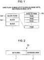
- a NAND flash memory allows data to be operated electrically, by "writing”, “reading” and “erasing".
- the minimum unit of writing/reading is a page PG
- the minimum unit of "erasing" is a block BLK as a collection of a plurality of pages.
- a page PG includes 512 bytes plus spare 16 bytes, thus 528 bytes or 4224 bits.
- a block BLK includes 32 pages of PG0 to PG31.
- each page PG of a NAND flash memory is made up of a data area 1 into which data is written, and a spare area 2 into which additional information is written.
- defect blocks exist at the time of shipment, and it is necessary to perform reading/writing from/to the NAND flash memory while avoiding these defect blocks.
- a NAND flash memory has the above-mentioned features. In this regard, it is desirable to allow existing file systems and tools to be used as they are, or only after slight modifications, with respect to the NAND flash memory as well.
- a layer for interpreting a request from the using side of the NAND flash memory for example, a file system, and translating the request into a command for operating the NAND flash memory (logical-physical translation layer).
- the non-volatile memory described in Japanese Unexamined Patent Application Publication No. 2003-36209 includes a mechanism for returning to the normal storage state even in the event of a system down during device operation such as a power outage. Also, the unit of logical address-physical address translation (logical-physical translation) in this non-volatile memory is a block size, and the write size is a block size.
- non-volatile memory described in Japanese Unexamined Patent Application Publication No. 2003-36209 mentioned above includes a mechanism for returning to the normal storage state even in the event of a system down during device operation such as a power outage, the unit of logical-physical translation is limited to the block size, and the write size is limited to the block size.
- the NAND flash memory described in Japanese Unexamined Patent Application Publication No. 2002-32256 allows for more efficient rewriting of data than is achieved by logical-physical translation in block units.
- US 2006/0059296 discloses a memory which is erased in units of pseudo-blocks which are smaller than the physical blocks. This is achieved by writing data in corresponding virtual blocks within the physical blocks, the virtual blocks and the physical blocks having a one-to-one relationship.
- each physical erase unit for the memory includes a plurality of segments each comprising a plurality of frames, which in turn comprises a plurality of pages.
- US 2007/005928 is concerned with the reduction of the time to write a non-volatile memory. This is achieved by changing the mapping between logical and physical addresses to ensure that each logical write operation causes data to be stored in a previously erased location.
- WO 02/058074 discloses the update of data in less than all pages of a non-volatile memory, by programming the new data in unused pages of the same or another block.
- EP 1 939 750 (an English language equivalent of WO 2007/033614 ) discloses the use of an unfinished state for checking a power cut off during writing.
- US 2006/0271725 discloses a non-volatile memory device wherein before use, the non-volatile means is divided into a plurality of sequentially addressed clusters, each cluster containing a plurality of sequentially addressed logical blocks or sections.
- a lookup table contains only the cluster addresses.
- a program for causing a computer to perform all the steps of a method according to the second aspect of the invention when the program is run on a computer.
- the unit of logical-physical translation can be selected from a size not smaller than a page size and not larger than a block size.
- management information necessary for logical-physical translation can be contained within the spare area while meeting the constraint placed on the writing order of pages within a non-volatile memory.
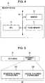
- Fig. 4 is a block diagram showing an example of the basic configuration of a memory device according to an embodiment of the present invention.
- a memory device 10 has a NAND flash memory 11 as a non-volatile memory, a memory 12 configured by, for example, a volatile memory such as a DRAM or an SRAM, and a CPU 13 as a control section.
- the NAND flash memory 11, the memory 12, and the CPU 13 are connected to each other via a bus 14.
- the NAND flash memory 11 has a memory cell array in which NAND strings with a plurality of memory cells connected in series are arranged in an arrayed fashion, and allows writing, reading, and erasing to be performed electrically.
- the minimum read/write unit of the NAND flash memory 11 is a page PG, and the minimum erase unit is a block BLK as a collection of a plurality of pages.
- a page PG includes 512 bytes data area plus 16 bytes spare area, thus 528 bytes or 4224 bits.
- a block BLK includes 32 pages of PG0 to PG31.
- the management of access to the NAND flash memory 11 is performed in accordance with control of the CPU 13 on the basis of management information, write complete data information, CRC information, or the like written into the spare area, as well as information of a logical-physical translation table (logical address-physical address translation table) or physical translation unit (TU) state map built in the memory 12.
- management information write complete data information, CRC information, or the like written into the spare area, as well as information of a logical-physical translation table (logical address-physical address translation table) or physical translation unit (TU) state map built in the memory 12.
- an access to the NAND flash memory 11 includes a memory access related to various write, read, and erase operations (including control processes corresponding to address translation, garbage collection, wear leveling, and the like).
- the memory 12 includes a ROM for program storage, and a RAM as a working memory.
- a logical-physical translation table (logical address-physical address translation table) described later in detail, and a physical (TU) state map are built.
- the CPU 13 functions as a control section that manages access to the NAND flash memory 11, on the basis of management information, write complete data, CRC information, or the like written into the spare area of the NAND flash memory 11, as well as information of a logical-physical translation table or a physical (TU) state map built in the memory 12.
- the CPU 13 manages access to the NAND flash memory by performing logical-physical translation in translation units (TU) each being an integer fraction of a block BLK and an integer multiple of the page size.
- TU logical-physical translation in translation units
- the CPU 13 has a function of performing an operation control in which, of the contents of a block, only physical TUs being currently used are all copied to another block with unused physical TUs, and then the source block is erased, thereby increasing unused physical TUs additionally by a number equal to the number of invalid physical TUs included in the source block.
- this operation is referred to as a fold operation.
- the CPU 13 builds a logical-physical translation table solely from information in the spare area of the NAND flash memory, and stores the logical-physical translation table into the memory 12.
- the CPU 13 writes state information indicating the completion of writing, and a CRC of management information in the spare area into the spare area of the NAND flash memory 11, thereby allowing recovery to a normal state from a power supply cutoff during writing to or erasing of the NAND flash memory 11.
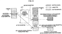
- Fig. 5 is a diagram showing an example of the basic configuration of a physical TU and a data structure related to management information stored in a spare area.
- a physical TU is made up of a data area 21 in which normal data is stored, and a spare area 23 in which at least management information 22 of the physical TU is stored.
- the management information 22 includes a corresponding logical TU address LTUN, and a sequential number SQN as writing-order information assigned to each block BLK.
- the spare area 23 has a sequential number storing area 231, and a logical TU number storing area 232.
- the sequential number storing area 231 and the logical TU number storing area 232 in the spare area 23 are referred to as management area.
- a block assigned with the latest sequential number is referred to as the latest block.
- Fig. 6 is a diagram illustrating the structure of data on the memory according to this embodiment.
- the structure of data on the memory for managing blocks, logical TUs, and physical TUs will be described.
- a logical-physical translation table LPTT On the memory 12, a logical-physical translation table LPTT, a physical TU state map STMP, and a sequential number table SQNT are formed.
- the logical-physical translation table LPTT is a table used for obtaining a corresponding physical TU number (address) PTUN from a logical TU number (address).
- the physical TU state map STMP is a map used for managing the state of each physical TU, and has four kinds of state: CLEAN, INUSE, DIRTY, and DEFECT.
- CLEAN represents an unwritten state after an erase operation.
- INUSE represents a state in which valid data referenced from the logical-physical translation table LPTT is stored (which can be said to be a valid (VALID) state).
- DIRTY represents a state in which invalid data not referenced from the logical-physical translation table LPTT is stored (which can be said to be an invalid (INVALID) state).
- DEFECT represents a state in which the physical TU in question exists within a defect block.
- the sequential number table SQNT is a table for storing sequential numbers SQN assigned to individual blocks.
- the sequential number table SQNT is used only at the time of the process of building the logical-physical translation table LPTT.
- the characteristic feature of the CPU 13 resides in logical-physical translation on a TU (translation unit) basis.
- Fig. 7 is a diagram showing the relationship between physical blocks, pages, and TUs of a NAND flash memory.
- the size of a TU is an integer fraction of the block size and an integer multiple of the page size.
- the actual TU on a NAND flash memory device is referred to as physical TU, and a TU provided to the using side after undergoing address translation according to an embodiment of the present invention is referred to as logical TU.
- the CPU 13 uses the logical-physical translation table LPTT that is a table used for obtaining a corresponding physical TU number (address) from a logical TU number (address).
- the CPU 13 basically has functions of performing reading of a logical TU, writing of a logical TU, a fold, and building of a logical-physical translation table. These functions will be described below.
- Fig. 8 is a diagram showing a read operation of a logical TU.
- the CPU 13 When reading a logical TU, as shown in Fig. 8 , the CPU 13 finds a physical TU number corresponding to a logical TU number from the logical-physical translation table LPTT, and reads the corresponding physical TU. Through the intermediation of the logical-physical translation table LPTT, a defect block can be avoided.
- Fig. 9 is a diagram showing a write operation of a logical TU.
- a physical TU P1 corresponds to a logical TU L1.
- the CPU 13 first writes data desired to be rewritten, into a physical TU P2 that has not been written yet (ST1 in Fig. 9 ).
- the CPU 13 makes the physical TU P2 into which data has been thus written correspond to the logical TU L1 of the logical-physical translation table LPTT (ST2 in Fig. 9 ).
- a state in which the latest data is stored as in the physical TU P2 is referred to as valid, and a state in which old data that is to be erased is stored as in the preceding physical TU P1 is referred to as invalid.
- Fig. 10 is a diagram showing a fold operation according to this embodiment.
- NAND flash memory 11 can be erased only on a block BLK basis, if there is another physical TU within a block BLK like the physical TU P1 in Fig. 9 , it is not possible to erase that physical TU even if the physical TU is invalid.
- the CPU 13 performs an operation of moving only valid physical TUs to a write target block BLK (ST11), and erasing the source block (ST12).
- this operation is referred to as a fold.
- the logical-physical translation table LPTT is information on the volatile memory 12, and is lost when power is turned off.
- the CPU 13 writes logical TU numbers into the spare area at the time of writing data into a physical TU so that, even in the above-mentioned case, the logical-physical translation table LPTT can be built from information on the NAND flash memory 11 after power is turned on.
- the CPU 13 builds the logical-physical translation table LPTT on the memory 12 by scanning management information in the spare area of each physical TU.
- the CPU 13 performs writing in order from the lowest-ordered block while assigning sequential numbers SQN as information indicating the writing order of blocks BLK, to individual blocks BLK.
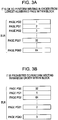
- the CPU 13 performs writing in order from a physical TU with the lowest physical TU number so that the writing order of pages within a block in Figs. 3A and 3B is met.
- the CPU 13 When writing to a physical TU, the CPU 13 records a sequential number SQN into the spare area in addition to a logical TU number.
- S is assigned as a sequential number SQN to a block BLK BLKm
- S+1 is assigned as a sequential number SQN to the next block BLK BLKm+1
- S+2 is assigned as a sequential number SQN to the next block BLK BLKm+2
- S+3 is assigned as a sequential number SQN to the next block BLK BLKm+3.
- the CPU 13 can uniquely find the writing order of physical TUs from sequential numbers SQN when building the logical-physical translation table LPTT, it is possible to determine the last written physical TU from among physical TUs having the same logical TU number, that is, a valid physical TU.
- Fig. 12 is a diagram showing an example of the relationship between a logical-physical translation table on the memory and management information (a logical TU number LTUN and a sequential number (SQN)) written in the spare area of each physical TU of the NAND flash memory.
- a logical-physical translation table on the memory and management information (a logical TU number LTUN and a sequential number (SQN)) written in the spare area of each physical TU of the NAND flash memory.
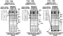
- Figs. 13A to 13C are diagrams showing how a logical-physical translation table is built by scanning the management information of the NAND flash memory in Fig. 12 in order from the physical TU0.
- Fig. 13A shows a state immediately after scanning of a block BLK0.
- the physical TU indicated by (*) is determined as DIRTY because a physical TU3 having the same logical TU number 4 is newer.
- Fig. 13B shows a state immediately after scanning of a block BLK1.
- the physical TU of the block BLK0 which is indicated by (*) is determined as DIRTY because a physical TU4 having the same logical TU number 1 is newer.
- Fig. 13C shows a state immediately after scanning of blocks BLK2, BLK3.
- the physical TU of the block BLK3 which is indicated by (*) is determined as DIRTY because a physical TU0 having the same logical TU number 5 is newer.
- the CPU 13 translates the number of a logical TU to be read, into a physical TU number by referencing the logical-physical translation table LPTT stored in the memory 12. Then, the CPU 13 identifies a physical TU from which data is to be read, and reads its data area.
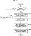
- Fig. 14 is a flowchart showing a data write operation.
- a physical TU is expressed as a PTU.
- the CPU 13 first determines whether or not a write target PTU is the last TU of a block (ST101).
- step ST101 If it is determined in step ST101 that a write target PTU is the last TU of a block, the CPU 13 selects one block that has not been written yet, and sets its first TU as a write target PTU (ST102).
- the CPU 13 updates the logical-physical translation table LPTT, and a physical TU state map STMP (ST105).
- step ST101 If it is determined in step ST101 that a write target PTU is not the last TU of a block, the processing proceeds not to step ST102 but to step ST106, and the write target PTU is advanced to the next physical TU, and the processing proceeds to step ST104.
- an unwritten block (block of which all physical TUs are CLEAN) is randomly selected, and the sequential number SQN is advanced by 1 step and written into that block (this physical TU set as a write target is referred to as write target PTU, and a block including the write target PTU is referred to as target block).
- step ST105 the logical-physical translation table LPTT and the physical TU state map are updated as follows.
- the state of a physical TU previously corresponding to a logical TU L in the logical-physical translation table LPTT is set to DIRTY, and the state of the write target PTU is set to INUSE.
- the write target PTU is made to correspond to the logical TU L.
- Fig. 15 is a flowchart showing a fold operation according to this embodiment.
- a physical TU on which fold processing is being performed is expressed as P.
- the CPU 13 selects a block including at least one DIRTY physical TU as a fold target block (ST111).
- step ST112 by specifying data and logical TU number read in step ST112, the read contents are written. In other words, writing of a logical TU is performed (ST113).
- the fold target block is erased.
- the logical-physical translation table LPTT and the physical TU state map STMP are data on the memory 12, and are lost when power is turned off.
- the logical-physical translation table LPTT and the physical TU state map STMP can be restored even in that case by scanning the management information (logical TU numbers LTUN and sequential numbers SQN) written into the spare area 23 of the NAND flash.
- Fig. 16 is a flowchart showing scanning of a spare area on a block by block basis, and a procedure for restoring a logical-physical translation table and a physical TU state map.
- the following processing is performed with respect to every block within a scan target block other than defect blocks.
- the CPU 13 reads the storing area (herein referred to as management area) 231, 232 of the management information 22 in the spare area 23 of the physical TU P1 (ST121).
- step ST122 If it is determined in step ST122 that the management area is unwritten, the state of the physical TU P1 is set to CLEAN (ST123).
- step ST122 If it is determined in step ST122 that the management area is not unwritten, the logical TU number of the management area of the physical TU P1 is set to L.
- the sequential number SQN in the management area is stored into the sequential number table SQNT (ST124).
- step ST125 If it is determined in step ST125 that no another physical TU P2 is registered, in the logical-physical translation table LPTT, the physical TU number P1 is made to correspond to the logical TU number L (ST126).
- step ST125 If it is determined in step ST125 that another physical TU P2 is registered, it is determined whether or not the physical TU P1 is newer than the physical TU P2 (ST128). This is determined from the sequential number SQN and the position within the block.
- step ST128 If it is determined in step ST128 that the physical TU P1 is newer than the physical TU P2, in the logical-physical translation table LPTT, the physical TU number P1 is made to correspond to the logical TU number L (ST129).
- the state of the physical TU P1 is set to INUSE, and the state of the physical TU P2 is set to DIRTY (ST130).
- step ST128 If it is determined in step ST128 that the physical TU P1 is not newer than the physical TU P2, the state of the physical TU P1 is set to DIRTY (ST131).
- the above-mentioned processing is performed with respect to every physical TU within the scan target block.
- the writing order can be determined from the sequential number and the position within the block.
- Figs. 17A and 17B are diagrams illustrating a process of determining whether physical TUs are new or old.
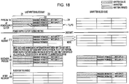
- Fig. 18 is a diagram showing an example of a power supply cutoff during writing and recovery process.
- state (write complete state) information 24 indicating completion of writing is additionally written into the spare area 23.
- the recovery process as shown in Fig. 18 is performed to erase the physical TU that is being currently written to.
- Fig. 19 is a diagram showing an example of a power supply cutoff during erasure and recovery process.
- a CRC 25 with respect to the management information 22 is added to the spare area 23.
- Fig. 19 illustrates that even when a power supply cutoff occurs during erasure and thus the data area 21 or the spare area 23 is left in an incorrect state, the block that was being erased is erased again by a recovery process.
- a physical TU within this block is determined as DIRTY or CLEAN as follows, in accordance with its erase state.
- the block BLK since the block BLK has no INUSE physical TU, the block BLK is erased. In the recovery process, a block not including any INUSE physical TU is erased.
- Fig. 20 is a flowchart of a write operation to a logical TU in a case where measures against a power supply cutoff are taken.
- the difference resides in adding a CRC to the management information to be written into the spare area, and providing, before the processing of step ST105, step ST107 in which immediately after writing of data and management information, a state indicating the completion of writing is additional written.
- Fig. 21 is a flowchart of a write operation of a logical TU in a case where measures against a power supply cutoff are taken.
- step ST132 in which, if the result of the determination in step ST122 is negative, it is determined whether or not write complete state information is correctly written in the spare area
- step ST133 in which, if it is determined that write complete state information is correctly written, it is determined whether or not the CRC of the spare area is correct.
- Fig. 22 is a flowchart showing a recovery process from a power supply cutoff during writing or erasure.
- the newest block is set as B1 and a physical TU in the newest block B1 which is not CLEAN and has the largest physical TU number is set as P1 (ST142).
- step ST143 If it is determined in step ST143 that the physical TU P1 is not DIRTY, it is determined whether or not the physical TU P1 is the last physical TU of the block B1 (ST144).
- step ST144 If it is determined in step ST144 that the physical TU P1 is not the last physical TU, a physical TU that is larger in physical TU number by 1 than the physical TU P1 is set as P2. Then, the entire data area 21 and spare area 23 of the physical TU P2 are read (ST145).
- step ST146 it is determined whether or not all bytes of the data thus read are in the "FFh” pattern. If it is determined in step ST146 that all bytes of the read data are in the "FFh” pattern, if it has been determined in step ST144 that the physical TU P1 is the last physical TU, the processing is terminated.
- step ST143 if it is determined in step ST143 that the physical TU P1 is DIRTY, or if it is determined in step ST146 that not all bytes of the read data are in the "FFh" pattern, the recovery process (relocate) of the block B1 is performed (ST147).
- step ST147 a recovery process (relocate) for a power supply cutoff during writing is performed.
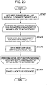
- Fig. 23 is a flowchart of a relocate process.
- the write target PTU is set to the last physical TU of the write target block (ST1471).
- the read contents are written (ST1473).
- step ST1471 the reason why the write target PTU is set as the last physical TU of a block in advance in step ST1471 is to set the first physical TU of an unwritten block as the physical TU from which writing is started in step ST1473.
- the CPU 13 manages access to the NAND flash memory 11 by performing logical-physical translation in translation units (TUs) each being an integer fraction of a block size and an integer multiple of a page size.
- the CPU 13 has the function of performing an operation control of copying, from among the contents of a source block, only all physical blocks being currently in use to another block having unused physical TUs, and erasing the source block, thereby increasing unused physical TUs additionally a number equal to the number of invalid physical TUs included in the source block.
- the CPU 13 has the function of writing a corresponding logical TU number, and a sequential number indicating the writing order of blocks into a spare area of the NAND flash memory, thereby building a logical-physical translation table solely from information in the spare area of the NAND flash memory at restart, and storing the logical-physical translation table into the memory 12. Therefore, the following advantages can be attained.
- the unit of logical-physical translation can be selected as a size not smaller than the page size but not larger than the block size. It is thus possible to realize logical-physical translation adapted to a unit as requested by the file system or the like.
- the utilization of the NAND flash can be enhanced (it is not necessary to use the data area of the NAND flash or to use an additional non-volatile memory to store information necessary for building management information such as a logical-physical translation table).
- the CPU 13 has the function of writing state information indicating the completion of writing and the CRC of management information in the spare area, into the spare area of the NAND flash memory 11, thus allowing recovery to the normal state from a power supply cutoff during writing to or erasing of the NAND flash memory 11. It is thus possible to provide a mechanism for returning to the normal storage state even in the event of a system down during writing to or erasing of the NAND flash due to a power outage or the like.
- the method described above in detail can be also configured such that the method is implemented as a program according to the above-mentioned procedure, and is executed by a computer such as a CPU.
- Such a program can be also configured such that the program is executed by being accessed from a computer in which a recording medium such as a semiconductor memory, a magnetic disc, an optical disc, or a floppy (R) disc is loaded.
- a recording medium such as a semiconductor memory, a magnetic disc, an optical disc, or a floppy (R) disc is loaded.
Landscapes
- Engineering & Computer Science (AREA)
- Theoretical Computer Science (AREA)
- Physics & Mathematics (AREA)
- General Engineering & Computer Science (AREA)
- General Physics & Mathematics (AREA)
- Memory System (AREA)
- Techniques For Improving Reliability Of Storages (AREA)
- Information Retrieval, Db Structures And Fs Structures Therefor (AREA)
Claims (11)
- Dispositif de mémoire (10), comprenant :une mémoire non volatile (11) qui permet d'écrire, de lire et d'effacer électriquement des données, et dans laquelle l'écriture et la lecture sont effectuées en unités d'une page (PAGE) et l'effacement est effectué en unités d'un bloc (BLK) comprenant une pluralité de pages (PAGE) ; etune section de commande (13) qui est configurée pour gérer l'accès à la mémoire non volatile (11), où la section de commande (13) est configurée pour effectuer une gestion de l'accès à la mémoire non volatile (11) en effectuant une traduction adresse logique-adresse physique (traduction logique-physique) dans des unités de traduction (TU), chacune étant une fraction entière d'une taille du bloc (BLK) et un multiple entier d'une taille de page,le dispositif de mémoire comprenant une mémoire supplémentaire (12), dans laquelle :une unité de traduction physique, TU, dans la mémoire non volatile (11) comprend une zone de données (21) et une zone de réserve (23) ; etla section de commande (13) est configurée :pour écrire des informations de gestion comprenant un numéro d'unité de traduction logique (LTUN) correspondant, et un numéro d'ordre (SQN) indiquant l'ordre d'écriture de chaque bloc (BLKm, BLKm+1, BLKm+2, BLKm+3), dans la zone de réserve (23) de la mémoire non volatile (11),pour construire une table de traduction logique-physique (LPTT) au démarrage en balayant les informations de gestion dans la zone de réserve (23) de la mémoire non volatile (11), et pour stocker la table de traduction logique-physique (LPTT) dans la mémoire supplémentaire (12), etpour exécuter un processus de traduction logique-physique sur la base de la table de traduction logique-physique de la mémoire supplémentaire (12) ;le dispositif de mémoire étant caractérisé en ce que :la section de commande (13) est configurée pour restaurer, au démarrage, une carte d'état d'unité de traduction physique (STMP) pour gérer l'unité de traduction physique (TU), parallèlement à la construction de la table de traduction logique-physique (LPTT) en balayant les informations de gestion dans la zone de réserve (23) de la mémoire non volatile (11) ; etla carte d'état de l'unité de traduction physique (STMP) indique si l'unité de traduction physique (TU) est dans un état non écrit, CLEAN, après une opération d'effacement, un état INUSE dans lequel des données valides référencées à partir de la table de traduction logique-physique sont stockées, ou un état INVALID dans lequel des données non valides non référencées à partir de la table de traduction logique-physique sont stockées, où :au cours de la restauration de la table de traduction logique-physique (LPTT) et de la carte d'état de l'unité de traduction physique (STMP), si une pluralité d'unités de traduction physique (TU) ayant le même numéro TU logique existent lors du balayage des informations de gestion dans la zone de réserve de la mémoire non volatile, la section de commande détermine, à partir du numéro d'ordre (SQN) et de la position dans le bloc, l'unité physique TU la plus récemment écrite comme étant INUSE, et détermine les autres unités de traduction (TU) physiques comme étant INVALID.
- Dispositif de mémoire selon la revendication 1, dans lequel :la section de commande (13) est configurée pour exécuter une opération de copie de contenus d'un bloc source d'uniquement toutes les unités de traduction physiques (TU) qui sont actuellement utilisées dans un bloc avec des unités de traduction physiques non utilisées (TU), et d'effacement du bloc source pour augmenter les unités de traduction physiques inutilisées (TU) d'un nombre égal au nombre d'unités de traduction physiques non valides (TU) incluses dans le bloc source.
- Dispositif de mémoire selon la revendication 2, dans lequel :lors de l'écriture d'un numéro d'unité de traduction logique (TU) dans la zone de réserve, la section de commande effectue une écriture sur une unité de traduction physique (TU) dans un bloc ayant le dernier numéro d'ordre (SQN), ladite unité de traduction physique étant l'unité TU physique CLEAN dont le numéro est le plus bas depuis sa dernière unité de traduction physique (TU).
- Dispositif de mémoire selon la revendication 3, dans lequel :si la dernière unité de traduction physique (TU) n'est pas CLEAN, la section de commande sélectionne de façon aléatoire un bloc qui n'a pas encore été écrit, incrémente le numéro d'ordre d'un pas, et écrit le numéro d'ordre dans le bloc.
- Dispositif de mémoire selon la revendication 4, dans lequel :la section de commande (13) est configurée pour mettre à jour la carte d'état de TU physique (STMP) en définissant un état d'une TU physique correspondant précédemment à une TU logique à INVALID, et en définissant un état de TU physique cible d'écriture à INUSE, et pour mettre à jour la table de traduction logique-physique (LPTT) en réécrivant sur la TU physique cible d'écriture.
- Dispositif de mémoire selon la revendication 1, dans lequel
la section de commande (11) est configurée pour déterminer si les unités de traduction physiques (TUs) sont nouvelles ou anciennes au moyen d'une comparaison de taille des numéros d'ordre (SQN) si les TUs physiques sont présentes dans différents blocs, et sur la base de numéros de TU physiques si les TUs physiques sont présentes dans le même bloc. - Dispositif de mémoire selon la revendication 1, dans lequel :lors de l'exécution d'une opération de pliage qui est une opération de copie de contenus d'un bloc source d'uniquement toutes les unités de traduction (TUs) physiques qui sont actuellement utilisées dans un bloc avec des unités de traduction physiques non utilisées (TUs), et d'effacement du bloc source pour augmenter les unités de traduction physiques inutilisées (TUs) d'un nombre égal au nombre d'unités de traduction physiques non valides (TUs) incluses dans le bloc source, la section de commande lit, par rapport à chaque TU INUSE dans un bloc cible plié, des données et des informations de gestion dans une unité de traduction physique (TU), et exécute une écriture d'une unité de traduction logique (TU) en spécifiant les données de lecture et un numéro d'unité de traduction (TU) logique, puis efface le bloc cible plié.
- Dispositif de mémoire selon la revendication 1, dans lequel :la section de commande (13) est configurée pour écrire des informations d'état d'achèvement d'écriture, qui permettent de déterminer si oui ou non l'écriture est terminée, dans la zone de réserve en plus des informations de gestion, etdéterminer si oui ou non une coupure d'alimentation électrique s'est produite lors de l'écriture, en vérifiant les informations d'état d'achèvement d'écriture au démarrage par rapport au dernier bloc ayant été écrit ayant le dernier numéro d'ordre.
- Dispositif de mémoire selon la revendication 1, dans lequel :la section de commande (13) est configurée pour écrire des informations indiquant si oui ou non les informations de gestion sont correctes dans la zone de réserve en plus des informations de gestion, etvérifier si oui ou non une valeur des informations de gestion est correcte en vérifiant, au démarrage, les informations indiquant si oui ou non les informations de gestion sont correctes.
- Procédé de gestion de mémoire pour un dispositif de mémoire (10) ayant une mémoire non volatile (11) qui permet d'écrire, de lire et d'effacer électriquement des données, et où l'écriture et la lecture sont effectuées en unités d'une page (PAGE) et l'effacement est effectué en unités d'un bloc (BLK) comprenant une pluralité de pages (PAGEs), comprenant les étapes suivantes :effectuer une traduction adresse logique-adresse physique (traduction logique-physique) dans des unités de traduction (TUs), chacune étant une fraction entière d'une taille du bloc et un multiple entier d'une taille de page ; etgérer l'accès à la mémoire non volatile (11) conformément à un résultat de la traduction logique-physique,où le dispositif de mémoire comprend en outre une mémoire supplémentaire (12), et oùune unité de traduction physique, TU, dans la mémoire non volatile (11) comprend une zone de données (21) et une zone de réserve (23) ; etle procédé comprend les étapes suivantes :écrire des informations de gestion comprenant un numéro de TU logique correspondant, et un numéro d'ordre (SQN) indiquant l'ordre d'écriture de chaque bloc, dans la zone de réserve de la mémoire non volatile (11),construire une table de traduction logique-physique (LPTT) au démarrage en balayant les informations de gestion dans la zone de réserve (23) de la mémoire non volatile (11), et stocker la table de traduction logique-physique (LPTT) dans la mémoire supplémentaire (12), etexécuter un processus de traduction logique-physique sur la base de la table de traduction logique-physique de la mémoire supplémentaire (12),le procédé de gestion de mémoire étant caractérisé par les étapes suivantes :restaurer, au démarrage, une carte d'état d'unité de traduction physique (STMP) pour gérer l'unité de traduction physique (TU), parallèlement à la construction de la table de traduction logique-physique (LPTT) en balayant les informations de gestion dans la zone de réserve (23) de la mémoire non volatile (11) ; oùla carte d'état de l'unité de traduction physique (STMP) indique si l'unité de traduction physique (TU) est dans un état non écrit, CLEAN, après une opération d'effacement, un état INUSE dans lequel des données valides référencées à partir de la table de traduction logique-physique sont stockées, ou un état INVALID dans lequel des données non valides non référencées à partir de la table de traduction logique-physique sont stockées, etau cours de la restauration de la table de traduction logique-physique (LPTT) et de la carte d'état de l'unité de traduction physique (STMP), si une pluralité d'unités de traduction physiques (TU) ayant le même numéro TU logique existent lors du balayage des informations de gestion dans la zone de réserve de la mémoire non volatile, déterminer, à partir du numéro d'ordre (SQN) et de la position dans le bloc, l'unité physique TUs la plus récemment écrite comme étant INUSE, et déterminer les autres unités de traduction physiques comme étant INVALID.
- Programme destiné à amener un ordinateur à exécuter toutes les étapes d'un procédé de gestion de mémoire selon la revendication 10 lorsque le programme est exécuté sur l'ordinateur.
Applications Claiming Priority (1)
| Application Number | Priority Date | Filing Date | Title |
|---|---|---|---|
| JP2007288726A JP4535117B2 (ja) | 2007-11-06 | 2007-11-06 | メモリ装置、メモリ管理方法、およびプログラム |
Publications (2)
| Publication Number | Publication Date |
|---|---|
| EP2058737A1 EP2058737A1 (fr) | 2009-05-13 |
| EP2058737B1 true EP2058737B1 (fr) | 2017-10-25 |
Family
ID=40219437
Family Applications (1)
| Application Number | Title | Priority Date | Filing Date |
|---|---|---|---|
| EP08253498.3A Ceased EP2058737B1 (fr) | 2007-11-06 | 2008-10-28 | Dispositif à mémoire non volatile, procédé de gestion de mémoire et programme |
Country Status (3)
| Country | Link |
|---|---|
| US (1) | US8205033B2 (fr) |
| EP (1) | EP2058737B1 (fr) |
| JP (1) | JP4535117B2 (fr) |
Families Citing this family (38)
| Publication number | Priority date | Publication date | Assignee | Title |
|---|---|---|---|---|
| JP5063337B2 (ja) * | 2007-12-27 | 2012-10-31 | 株式会社日立製作所 | 半導体装置 |
| US8495423B2 (en) * | 2009-08-11 | 2013-07-23 | International Business Machines Corporation | Flash-based memory system with robust backup and restart features and removable modules |
| JP2011154547A (ja) * | 2010-01-27 | 2011-08-11 | Toshiba Corp | メモリ管理装置及びメモリ管理方法 |
| US20120173795A1 (en) * | 2010-05-25 | 2012-07-05 | Ocz Technology Group, Inc. | Solid state drive with low write amplification |
| JP5464066B2 (ja) * | 2010-06-10 | 2014-04-09 | ソニー株式会社 | 通信装置、及び、通信方法 |
| US8682639B2 (en) * | 2010-09-21 | 2014-03-25 | Texas Instruments Incorporated | Dedicated memory window for emulation address |
| JP2012133655A (ja) * | 2010-12-22 | 2012-07-12 | Sony Corp | 管理装置、管理方法、およびプログラム |
| JP2012173778A (ja) * | 2011-02-17 | 2012-09-10 | Sony Corp | 管理装置、および管理方法 |
| US9424125B2 (en) * | 2013-01-16 | 2016-08-23 | Google Inc. | Consistent, disk-backed arrays |
| TWI503841B (zh) * | 2013-04-26 | 2015-10-11 | Phison Electronics Corp | 寫入方法、記憶體控制器與記憶體儲存裝置 |
| US10956050B2 (en) | 2014-03-31 | 2021-03-23 | Sandisk Enterprise Ip Llc | Methods and systems for efficient non-isolated transactions |
| US9916356B2 (en) | 2014-03-31 | 2018-03-13 | Sandisk Technologies Llc | Methods and systems for insert optimization of tiered data structures |
| US9928169B2 (en) | 2014-05-07 | 2018-03-27 | Sandisk Technologies Llc | Method and system for improving swap performance |
| US9633233B2 (en) | 2014-05-07 | 2017-04-25 | Sandisk Technologies Llc | Method and computing device for encrypting data stored in swap memory |
| US9665296B2 (en) | 2014-05-07 | 2017-05-30 | Sandisk Technologies Llc | Method and computing device for using both volatile memory and non-volatile swap memory to pre-load a plurality of applications |
| US20150324132A1 (en) * | 2014-05-07 | 2015-11-12 | Sandisk Technologies Inc. | Method and Computing Device for Fast Erase of Swap Memory |
| US9710198B2 (en) | 2014-05-07 | 2017-07-18 | Sandisk Technologies Llc | Method and computing device for controlling bandwidth of swap operations |
| JP2016012166A (ja) | 2014-06-27 | 2016-01-21 | 富士通株式会社 | ストレージ管理装置,ストレージ管理プログラム,及び制御方法 |
| KR102263046B1 (ko) | 2014-10-29 | 2021-06-09 | 삼성전자주식회사 | 메모리 장치, 메모리 시스템, 상기 메모리 장치의 동작 방법 및 상기 메모리 시스템의 동작 방법 |
| KR102252378B1 (ko) | 2014-10-29 | 2021-05-14 | 삼성전자주식회사 | 메모리 장치, 메모리 시스템, 상기 메모리 장치의 동작 방법 및 상기 메모리 시스템의 동작 방법 |
| KR102287760B1 (ko) | 2014-10-29 | 2021-08-09 | 삼성전자주식회사 | 메모리 시스템 및 상기 메모리 시스템의 동작 방법 |
| US10133764B2 (en) | 2015-09-30 | 2018-11-20 | Sandisk Technologies Llc | Reduction of write amplification in object store |
| US9619165B1 (en) * | 2015-10-30 | 2017-04-11 | Sandisk Technologies Llc | Convertible leaf memory mapping |
| US10185658B2 (en) | 2016-02-23 | 2019-01-22 | Sandisk Technologies Llc | Efficient implementation of optimized host-based garbage collection strategies using xcopy and multiple logical stripes |
| US10747676B2 (en) | 2016-02-23 | 2020-08-18 | Sandisk Technologies Llc | Memory-efficient object address mapping in a tiered data structure |
| US10289340B2 (en) | 2016-02-23 | 2019-05-14 | Sandisk Technologies Llc | Coalescing metadata and data writes via write serialization with device-level address remapping |
| US9983820B2 (en) * | 2016-03-29 | 2018-05-29 | Nxp B.V. | Method for performing data updates |
| FR3051574A1 (fr) * | 2016-05-20 | 2017-11-24 | Proton World Int Nv | Gestion du stockage dans une memoire flash |
| FR3051590A1 (fr) * | 2016-05-20 | 2017-11-24 | Proton World Int Nv | Compteur en memoire flash |
| JP2018028830A (ja) * | 2016-08-19 | 2018-02-22 | 三菱電機株式会社 | 電子制御装置およびその情報記憶方法 |
| FR3055992A1 (fr) | 2016-09-09 | 2018-03-16 | Proton World International N.V. | Gestion d'index dans une memoire flash |
| FR3072476A1 (fr) | 2017-10-13 | 2019-04-19 | Proton World International N.V. | Unite logique de memoire pour memoire flash |
| JP6675466B2 (ja) * | 2018-11-13 | 2020-04-01 | キオクシア株式会社 | メモリシステム |
| KR102693311B1 (ko) | 2018-12-20 | 2024-08-09 | 삼성전자주식회사 | 스토리지 장치의 데이터 기입 방법 및 이를 수행하는 스토리지 장치 |
| CN112148365B (zh) * | 2019-06-26 | 2024-04-05 | 珠海零边界集成电路有限公司 | 一种控制模块、方法及微控制器芯片 |
| CN113311989B (zh) * | 2020-02-26 | 2023-09-22 | 北京君正集成电路股份有限公司 | 一种基于并行使用的双片nand flash坏块管理方法 |
| CN113391755B (zh) * | 2020-02-26 | 2023-09-22 | 北京君正集成电路股份有限公司 | 一种并行双片nand flash中物理擦除块动态关联的方法 |
| US20250217282A1 (en) * | 2023-12-29 | 2025-07-03 | Micron Technology, Inc. | Address mapping table for a memory sub-system using mixed translation unit sizes |
Citations (1)
| Publication number | Priority date | Publication date | Assignee | Title |
|---|---|---|---|---|
| US20060271725A1 (en) * | 2005-05-24 | 2006-11-30 | Micron Technology, Inc. | Version based non-volatile memory translation layer |
Family Cites Families (21)
| Publication number | Priority date | Publication date | Assignee | Title |
|---|---|---|---|---|
| US5603001A (en) * | 1994-05-09 | 1997-02-11 | Kabushiki Kaisha Toshiba | Semiconductor disk system having a plurality of flash memories |
| US6278678B1 (en) * | 1999-02-12 | 2001-08-21 | Sony Corporation | Editing apparatus, editing method, and recording medium |
| JP2002032256A (ja) | 2000-07-19 | 2002-01-31 | Matsushita Electric Ind Co Ltd | 端末装置 |
| US6763424B2 (en) * | 2001-01-19 | 2004-07-13 | Sandisk Corporation | Partial block data programming and reading operations in a non-volatile memory |
| JP3675375B2 (ja) | 2001-07-25 | 2005-07-27 | ソニー株式会社 | 不揮発性メモリ並びに不揮発性メモリのデータ書き換え方法 |
| EP1514189A1 (fr) * | 2002-06-20 | 2005-03-16 | Tokyo Electron Device Limited | Memoire flash |
| US7062577B2 (en) * | 2002-12-18 | 2006-06-13 | Lsi Logic Corporation | AMBA slave modular bus interfaces |
| US7012835B2 (en) * | 2003-10-03 | 2006-03-14 | Sandisk Corporation | Flash memory data correction and scrub techniques |
| JP4242245B2 (ja) * | 2003-10-06 | 2009-03-25 | 株式会社ワークビット | フラッシュrom制御装置 |
| KR100608602B1 (ko) * | 2003-12-10 | 2006-08-03 | 삼성전자주식회사 | 플래시 메모리, 이를 위한 사상 제어 장치 및 방법 |
| US7281114B2 (en) * | 2003-12-26 | 2007-10-09 | Tdk Corporation | Memory controller, flash memory system, and method of controlling operation for data exchange between host system and flash memory |
| JP2005267676A (ja) * | 2004-03-16 | 2005-09-29 | Matsushita Electric Ind Co Ltd | 不揮発性記憶装置 |
| KR20070060101A (ko) * | 2004-08-30 | 2007-06-12 | 실리콘 스토리지 테크놀로지 인크 | 무선 단말기에서의 비휘발성 메모리 관리 시스템 및 방법 |
| US20060059296A1 (en) * | 2004-09-16 | 2006-03-16 | M-Systems Flash Disk Pioneers, Ltd. | Emulating small block size of flash memory |
| US7849253B2 (en) * | 2005-04-04 | 2010-12-07 | Standard Microsystems Corporation | Method for fast access to flash-memory media |
| US7797479B2 (en) * | 2005-06-30 | 2010-09-14 | Intel Corporation | Technique to write to a non-volatile memory |
| TW200705180A (en) * | 2005-07-29 | 2007-02-01 | Genesys Logic Inc | Adjustable flash memory management system and method |
| CN100573476C (zh) * | 2005-09-25 | 2009-12-23 | 深圳市朗科科技股份有限公司 | 闪存介质数据管理方法 |
| JP4501881B2 (ja) * | 2006-03-23 | 2010-07-14 | Tdk株式会社 | メモリコントローラ及びフラッシュメモリシステム |
| JP2007288726A (ja) | 2006-04-20 | 2007-11-01 | Matsushita Electric Ind Co Ltd | 撮像装置 |
| US7983465B2 (en) * | 2007-05-09 | 2011-07-19 | Société De Commercialisation Des Produits De La Recherche Appliquée - Socpra Sciences Santé Et Humaines, S.E.C. | Image reconstruction methods based on block circulant system matrices |
-
2007
- 2007-11-06 JP JP2007288726A patent/JP4535117B2/ja not_active Expired - Fee Related
-
2008
- 2008-10-28 EP EP08253498.3A patent/EP2058737B1/fr not_active Ceased
- 2008-11-05 US US12/265,324 patent/US8205033B2/en not_active Expired - Fee Related
Patent Citations (1)
| Publication number | Priority date | Publication date | Assignee | Title |
|---|---|---|---|---|
| US20060271725A1 (en) * | 2005-05-24 | 2006-11-30 | Micron Technology, Inc. | Version based non-volatile memory translation layer |
Also Published As
| Publication number | Publication date |
|---|---|
| EP2058737A1 (fr) | 2009-05-13 |
| JP2009116601A (ja) | 2009-05-28 |
| JP4535117B2 (ja) | 2010-09-01 |
| US8205033B2 (en) | 2012-06-19 |
| US20090119450A1 (en) | 2009-05-07 |
Similar Documents
| Publication | Publication Date | Title |
|---|---|---|
| EP2058737B1 (fr) | Dispositif à mémoire non volatile, procédé de gestion de mémoire et programme | |
| CN101169751B (zh) | 具有闪存设备的系统及其数据恢复方法 | |
| EP1739683B1 (fr) | Gestion de l'espace pour la gestion de la mémoire non volatile de haute capacité | |
| USRE45222E1 (en) | Method of writing of writing to a flash memory including data blocks and log blocks, using a logical address having a block address portion and page identifying portion, a block address table and a page table | |
| JP4132086B2 (ja) | フラッシュメモリ内のブロックにおける移動セクタ | |
| EP1228510B1 (fr) | Gestion d'espace pour la gestion d'une memoire non volatile haute capacite | |
| US7783851B2 (en) | Methods of reusing log blocks in non-volatile memories and related non-volatile memory devices | |
| US7979626B2 (en) | Flash recovery employing transaction log | |
| US7340581B2 (en) | Method of writing data to non-volatile memory | |
| KR100493732B1 (ko) | 비휘발성 메모리내의 코드/데이터 경계를 조정가능하게하는 장치 및 방법 | |
| US20080120488A1 (en) | Apparatus and method of managing nonvolatile memory | |
| US20100169540A1 (en) | Method and apparatus for relocating selected data between flash partitions in a memory device | |
| US20080104357A1 (en) | Apparatus and method for managing nonvolatile memory | |
| US8694718B2 (en) | Wear leveling for erasable memories | |
| JP4046877B2 (ja) | 一括消去型不揮発性メモリおよび携帯電話 | |
| JP2013061799A (ja) | 記憶装置、記憶装置の制御方法およびコントローラ | |
| US7664906B2 (en) | Flash memory access apparatus and method | |
| US7558904B2 (en) | Controller, data memory system, data rewriting method, and computer program product | |
| CN109669889B (zh) | 一种轻量型Nor Flash闪存控制方法和装置 | |
| JP4242245B2 (ja) | フラッシュrom制御装置 | |
| CN116540950B (zh) | 一种存储器件及其写入数据的控制方法 | |
| JP2003058417A (ja) | 記憶装置 | |
| CN1311327C (zh) | 成块可擦存储器的管理数据组的复原方法 | |
| US20070005929A1 (en) | Method, system, and article of manufacture for sector mapping in a flash device | |
| CN105825082A (zh) | 数据储存装置以及快闪存储器控制方法 |
Legal Events
| Date | Code | Title | Description |
|---|---|---|---|
| PUAI | Public reference made under article 153(3) epc to a published international application that has entered the european phase |
Free format text: ORIGINAL CODE: 0009012 |
|
| 17P | Request for examination filed |
Effective date: 20081106 |
|
| AK | Designated contracting states |
Kind code of ref document: A1 Designated state(s): AT BE BG CH CY CZ DE DK EE ES FI FR GB GR HR HU IE IS IT LI LT LU LV MC MT NL NO PL PT RO SE SI SK TR |
|
| AX | Request for extension of the european patent |
Extension state: AL BA MK RS |
|
| AKX | Designation fees paid |
Designated state(s): DE FR GB |
|
| 17Q | First examination report despatched |
Effective date: 20100215 |
|
| STAA | Information on the status of an ep patent application or granted ep patent |
Free format text: STATUS: EXAMINATION IS IN PROGRESS |
|
| GRAP | Despatch of communication of intention to grant a patent |
Free format text: ORIGINAL CODE: EPIDOSNIGR1 |
|
| STAA | Information on the status of an ep patent application or granted ep patent |
Free format text: STATUS: GRANT OF PATENT IS INTENDED |
|
| INTG | Intention to grant announced |
Effective date: 20170613 |
|
| GRAS | Grant fee paid |
Free format text: ORIGINAL CODE: EPIDOSNIGR3 |
|
| GRAA | (expected) grant |
Free format text: ORIGINAL CODE: 0009210 |
|
| STAA | Information on the status of an ep patent application or granted ep patent |
Free format text: STATUS: THE PATENT HAS BEEN GRANTED |
|
| AK | Designated contracting states |
Kind code of ref document: B1 Designated state(s): DE FR GB |
|
| REG | Reference to a national code |
Ref country code: GB Ref legal event code: FG4D |
|
| REG | Reference to a national code |
Ref country code: FR Ref legal event code: PLFP Year of fee payment: 10 |
|
| REG | Reference to a national code |
Ref country code: DE Ref legal event code: R096 Ref document number: 602008052624 Country of ref document: DE |
|
| REG | Reference to a national code |
Ref country code: DE Ref legal event code: R097 Ref document number: 602008052624 Country of ref document: DE |
|
| PLBE | No opposition filed within time limit |
Free format text: ORIGINAL CODE: 0009261 |
|
| STAA | Information on the status of an ep patent application or granted ep patent |
Free format text: STATUS: NO OPPOSITION FILED WITHIN TIME LIMIT |
|
| 26N | No opposition filed |
Effective date: 20180726 |
|
| REG | Reference to a national code |
Ref country code: FR Ref legal event code: PLFP Year of fee payment: 11 |
|
| PGFP | Annual fee paid to national office [announced via postgrant information from national office to epo] |
Ref country code: DE Payment date: 20201022 Year of fee payment: 13 Ref country code: FR Payment date: 20201022 Year of fee payment: 13 Ref country code: GB Payment date: 20201022 Year of fee payment: 13 |
|
| REG | Reference to a national code |
Ref country code: DE Ref legal event code: R119 Ref document number: 602008052624 Country of ref document: DE |
|
| GBPC | Gb: european patent ceased through non-payment of renewal fee |
Effective date: 20211028 |
|
| PG25 | Lapsed in a contracting state [announced via postgrant information from national office to epo] |
Ref country code: GB Free format text: LAPSE BECAUSE OF NON-PAYMENT OF DUE FEES Effective date: 20211028 Ref country code: DE Free format text: LAPSE BECAUSE OF NON-PAYMENT OF DUE FEES Effective date: 20220503 |
|
| PG25 | Lapsed in a contracting state [announced via postgrant information from national office to epo] |
Ref country code: FR Free format text: LAPSE BECAUSE OF NON-PAYMENT OF DUE FEES Effective date: 20211031 |