EP2059020A2 - Capteur d'images, système de prise d'images, et méthode de contrôle d'un capteur d'images - Google Patents
Capteur d'images, système de prise d'images, et méthode de contrôle d'un capteur d'images Download PDFInfo
- Publication number
- EP2059020A2 EP2059020A2 EP08166105A EP08166105A EP2059020A2 EP 2059020 A2 EP2059020 A2 EP 2059020A2 EP 08166105 A EP08166105 A EP 08166105A EP 08166105 A EP08166105 A EP 08166105A EP 2059020 A2 EP2059020 A2 EP 2059020A2
- Authority
- EP
- European Patent Office
- Prior art keywords
- shift register
- region
- period
- scans
- signal
- Prior art date
- Legal status (The legal status is an assumption and is not a legal conclusion. Google has not performed a legal analysis and makes no representation as to the accuracy of the status listed.)
- Granted
Links
- 238000000034 method Methods 0.000 title claims description 17
- 238000003384 imaging method Methods 0.000 title claims description 8
- 230000003287 optical effect Effects 0.000 claims abstract description 33
- 238000012545 processing Methods 0.000 claims description 11
- 238000012546 transfer Methods 0.000 claims description 4
- 101100481702 Arabidopsis thaliana TMK1 gene Proteins 0.000 claims description 3
- 230000004044 response Effects 0.000 claims description 3
- 238000010586 diagram Methods 0.000 description 5
- 230000006870 function Effects 0.000 description 4
- 101100178269 Schizosaccharomyces pombe (strain 972 / ATCC 24843) hob1 gene Proteins 0.000 description 3
- 101100178270 Schizosaccharomyces pombe (strain 972 / ATCC 24843) hob3 gene Proteins 0.000 description 3
- 101100481703 Arabidopsis thaliana TMK2 gene Proteins 0.000 description 2
- 238000012937 correction Methods 0.000 description 2
- 101100481704 Arabidopsis thaliana TMK3 gene Proteins 0.000 description 1
- 238000006243 chemical reaction Methods 0.000 description 1
- 238000012986 modification Methods 0.000 description 1
- 230000004048 modification Effects 0.000 description 1
- 238000004904 shortening Methods 0.000 description 1
Images





Classifications
-
- H—ELECTRICITY
- H04—ELECTRIC COMMUNICATION TECHNIQUE
- H04N—PICTORIAL COMMUNICATION, e.g. TELEVISION
- H04N23/00—Cameras or camera modules comprising electronic image sensors; Control thereof
- H04N23/60—Control of cameras or camera modules
- H04N23/68—Control of cameras or camera modules for stable pick-up of the scene, e.g. compensating for camera body vibrations
-
- H—ELECTRICITY
- H04—ELECTRIC COMMUNICATION TECHNIQUE
- H04N—PICTORIAL COMMUNICATION, e.g. TELEVISION
- H04N23/00—Cameras or camera modules comprising electronic image sensors; Control thereof
- H04N23/60—Control of cameras or camera modules
- H04N23/68—Control of cameras or camera modules for stable pick-up of the scene, e.g. compensating for camera body vibrations
- H04N23/682—Vibration or motion blur correction
- H04N23/684—Vibration or motion blur correction performed by controlling the image sensor readout, e.g. by controlling the integration time
- H04N23/6842—Vibration or motion blur correction performed by controlling the image sensor readout, e.g. by controlling the integration time by controlling the scanning position, e.g. windowing
-
- H—ELECTRICITY
- H04—ELECTRIC COMMUNICATION TECHNIQUE
- H04N—PICTORIAL COMMUNICATION, e.g. TELEVISION
- H04N25/00—Circuitry of solid-state image sensors [SSIS]; Control thereof
- H04N25/40—Extracting pixel data from image sensors by controlling scanning circuits, e.g. by modifying the number of pixels sampled or to be sampled
- H04N25/44—Extracting pixel data from image sensors by controlling scanning circuits, e.g. by modifying the number of pixels sampled or to be sampled by partially reading an SSIS array
-
- H—ELECTRICITY
- H04—ELECTRIC COMMUNICATION TECHNIQUE
- H04N—PICTORIAL COMMUNICATION, e.g. TELEVISION
- H04N25/00—Circuitry of solid-state image sensors [SSIS]; Control thereof
- H04N25/60—Noise processing, e.g. detecting, correcting, reducing or removing noise
- H04N25/63—Noise processing, e.g. detecting, correcting, reducing or removing noise applied to dark current
- H04N25/633—Noise processing, e.g. detecting, correcting, reducing or removing noise applied to dark current by using optical black pixels
-
- H—ELECTRICITY
- H04—ELECTRIC COMMUNICATION TECHNIQUE
- H04N—PICTORIAL COMMUNICATION, e.g. TELEVISION
- H04N25/00—Circuitry of solid-state image sensors [SSIS]; Control thereof
- H04N25/60—Noise processing, e.g. detecting, correcting, reducing or removing noise
- H04N25/67—Noise processing, e.g. detecting, correcting, reducing or removing noise applied to fixed-pattern noise, e.g. non-uniformity of response
- H04N25/671—Noise processing, e.g. detecting, correcting, reducing or removing noise applied to fixed-pattern noise, e.g. non-uniformity of response for non-uniformity detection or correction
- H04N25/677—Noise processing, e.g. detecting, correcting, reducing or removing noise applied to fixed-pattern noise, e.g. non-uniformity of response for non-uniformity detection or correction for reducing the column or line fixed pattern noise
-
- H—ELECTRICITY
- H04—ELECTRIC COMMUNICATION TECHNIQUE
- H04N—PICTORIAL COMMUNICATION, e.g. TELEVISION
- H04N25/00—Circuitry of solid-state image sensors [SSIS]; Control thereof
- H04N25/70—SSIS architectures; Circuits associated therewith
- H04N25/71—Charge-coupled device [CCD] sensors; Charge-transfer registers specially adapted for CCD sensors
- H04N25/74—Circuitry for scanning or addressing the pixel array
-
- H—ELECTRICITY
- H04—ELECTRIC COMMUNICATION TECHNIQUE
- H04N—PICTORIAL COMMUNICATION, e.g. TELEVISION
- H04N25/00—Circuitry of solid-state image sensors [SSIS]; Control thereof
- H04N25/70—SSIS architectures; Circuits associated therewith
- H04N25/76—Addressed sensors, e.g. MOS or CMOS sensors
- H04N25/779—Circuitry for scanning or addressing the pixel array
-
- H—ELECTRICITY
- H04—ELECTRIC COMMUNICATION TECHNIQUE
- H04N—PICTORIAL COMMUNICATION, e.g. TELEVISION
- H04N25/00—Circuitry of solid-state image sensors [SSIS]; Control thereof
- H04N25/70—SSIS architectures; Circuits associated therewith
- H04N25/76—Addressed sensors, e.g. MOS or CMOS sensors
- H04N25/7795—Circuitry for generating timing or clock signals
Definitions
- the present invention relates to an image sensing apparatus, imaging system, and image sensing apparatus driving method.
- Previously proposed conventional image sensing apparatus has a pixel array including an optical black region and effective pixel region (see Japanese Patent Laid-Open No. 2001-45383 ).
- a shift register for scanning the respective rows or columns of the pixel array is formed from a plurality of circuit blocks.
- a decoder circuit for selecting one of the circuit blocks is arranged on the input side of the shift register. By selecting a circuit block by the decoder circuit, scanning of pixels can start for each pixel block including a plurality of pixels in an effective pixel region.
- image sensing apparatuses such as a video camera and still camera require a high-precision electronic anti-shake (camera shake correction) function.
- the present inventor has examined to shift a readout region, which is a partial region of the effective pixel region, in the direction of camera shake in the effective pixel region.
- the readout start position of the readout region is changed for each pixel (for each row and each column) in the effective pixel region.
- the readout start position of the readout region can be changed for each pixel in the effective pixel region.
- the size of a circuit for scanning the pixel array may become large, complicating the arrangement of the image sensing apparatus.
- the present invention provides an image sensing apparatus, imaging system, and image sensing apparatus driving method capable of shortening, by a simple arrangement, the period until scanning of the readout region starts for each pixel in the effective pixel region after the end of scanning the optical black region.
- the present invention in its first aspect provides an image sensing apparatus as specified in claims 1 to 3.
- the present invention in its second aspect provides an image sensing apparatus as specified in claims 4 to 6.
- the present invention in its third aspect provides an imaging system as specified in claim 7.
- the present invention in its fourth aspect provides a method of driving an image sensing apparatus as specified in claims 8 and 9.
- the present invention in its fifth aspect provides a method of driving an image sensing apparatus as specified in claims 10 and 11.
- Fig. 1 is a view of the arrangement of an image sensing apparatus 100 according to the first embodiment of the present invention
- Fig. 2 is a view for explaining a readout region RR1 in an effective pixel region 03;
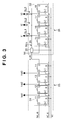
- Fig. 3 is a circuit diagram of a horizontal shift register unit
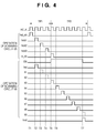
- Fig. 4 is a timing chart showing the detailed operation of a scanning unit 30
- Fig. 5 is a block diagram of an imaging system to which the image sensing apparatus according to the first embodiment is applied;
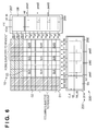
- Fig. 6 is a view of the arrangement of an image sensing apparatus 200 according to the second embodiment of the present invention.
- Fig. 7 is a view for explaining a readout region RR201 in an effective pixel region 03;
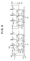
- Fig. 8 is a circuit diagram of a horizontal shift register unit
- Fig. 9 is a timing chart showing the detailed operation of a scanning unit 230.
- Fig. 1 is a view of the arrangement of the image sensing apparatus 100 according to the first embodiment of the present invention.
- the image sensing apparatus 100 comprises a pixel array 10 and scanning unit 30.
- the pixel array 10 has an optical black (to be referred to as OB hereinafter) region 02 and an effective pixel region 03.
- OB optical black
- the OB region 02 is shielded from light, and includes a plurality of elements for reading out a reference signal for the black level.
- the OB region 02 is formed by three columns from the left end or three rows from the upper end of the pixel array 10.
- the element can be one which has the same structure as that of an effective pixel and is shielded from light.
- the element is one which does not have a region corresponding to the photoelectric conversion unit (e.g., photodiode) of an effective pixel or has a small volume of a region where the signal charges of the photodiode are stored.
- the effective pixel region 03 includes a plurality of pixels which receive light corresponding to the optical image of an object and from which a pixel signal obtained by photoelectrically converting the light is read out.
- the effective pixel region 03 is a region of 9 rows ⁇ 9 columns from the lower and right ends of the pixel array 10.
- the scanning unit 30 scans the pixel array 10 to drive respective pixels.
- the scanning unit 30 includes a horizontal shift register unit 04 and vertical shift register unit 07.
- the horizontal shift register unit 04 horizontally scans the respective columns of the pixel array 10.
- the vertical shift register unit 07 vertically scans the respective rows of the pixel array 10.
- the horizontal shift register unit 04 includes a first horizontal scanning circuit 05 and second horizontal scanning circuit 06.
- the first horizontal scanning circuit 05 sequentially scans the respective columns of a region extending in the vertical direction in the OB region 02.
- the second horizontal scanning circuit 06 sequentially scans the respective columns of the effective pixel region 03 in accordance with horizontal scan signals h1 to h9.
- the first horizontal scanning circuit 05 and second horizontal scanning circuit 06 commonly receive a clock signal HCLK and reset signal hrst.
- the first horizontal scanning circuit 05 and second horizontal scanning circuit 06 receive a first start signal hst_ob and second start signal hst, respectively.
- the second horizontal scanning circuit 06 receives an end notification signal e_ob from the first horizontal scanning circuit 05. Since two start signals (start pulses) are respectively used for the first horizontal scanning circuit 05 and second horizontal scanning circuit 06, the OB region 02 and effective pixel region 03 can be independently scanned.
- the vertical shift register unit 07 includes a first vertical scanning circuit 08 and second vertical scanning circuit 09.
- the first vertical scanning circuit 08 sequentially scans the respective rows of a region extending in the horizontal direction in the OB region 02.
- the second vertical scanning circuit 09 sequentially scans the respective rows of the effective pixel region 03 in accordance with vertical scan signals v1 to v9.
- the first vertical scanning circuit 08 and second vertical scanning circuit 09 commonly receive a clock signal VCLK and reset signal vrst.
- the first vertical scanning circuit 08 and second vertical scanning circuit 09 receive a start signal (first start signal) vst_ob and start signal (second start signal) vst, respectively.
- the second vertical scanning circuit 09 receives an end notification signal e_ob from the first vertical scanning circuit 08. Since two start signals (start pulses) are respectively used for the first vertical scanning circuit 08 and second vertical scanning circuit 09, the OB region 02 and effective pixel region 03 can be independently scanned.
- Fig. 2 is a view for explaining a readout region RR1 in the effective pixel region 03.
- Fig. 3 is a circuit diagram of the horizontal shift register unit. Although the horizontal shift register unit 04 will be mainly explained, the following description also applies to the vertical shift register unit 07.
- the horizontal shift register unit 04 includes the first horizontal scanning circuit 05 and second horizontal scanning circuit 06.
- the first horizontal scanning circuit 05 includes a first shift register 31.
- the first shift register 31 includes a plurality of flip-flops 11 to 14.
- the first shift register 31 receives the first start signal hst_ob, clock signal HCLK, and reset signal hrst via an input terminal D, clock terminal C, and reset terminal R of each flip-flop, respectively.
- the first shift register 31 Upon receiving the reset signal hrst, the first shift register 31 is reset in synchronism with the clock signal HCLK.
- An output terminal Q of each of the flip-flops 11 to 14 is connected to pixels on each column of a region RR2 extending in the vertical direction in the OB region 02.
- the first shift register 31 Upon receiving the first start signal hst_ob, the first shift register 31 shifts the first start signal hst_ob in synchronism with the clock signal HCLK, sequentially scanning the respective columns of the region RR2 extending in the vertical direction in the OB region 02. That is, the first shift register 31 supplies the horizontal scan signals hob1 to hob3 to the respective columns of the pixel array 10.
- the first shift register 31 After the end of scanning the OB region 02, the first shift register 31 outputs the end notification signal e_ob to an enable circuit 20 (to be described later). That is, upon completion of scanning the OB region 02, the first shift register 31 controls the enable circuit 20 to enable a plurality of signal lines SL1, SL2, SL3, ....
- the second horizontal scanning circuit 06 includes a second shift register 32, the plurality of signal lines SL1, SL2, SL3, ..., and the enable circuit 20.
- the second shift register 32 includes a plurality of flip-flops (e.g., D flip-flops) 15, 16, 17, 18, ....
- the second shift register 32 receives the second start signal hst, clock signal HCLK, and reset signal hrst via the input terminal D, clock terminal C, and reset terminal R of each flip-flop, respectively.
- the second shift register 32 Upon receiving the reset signal hrst, the second shift register 32 is reset in synchronism with the clock signal HCLK.
- the plurality of signal lines SL1, SL2, SL3, ... connect the second shift register 32 to the pixel array 10. That is, the output terminal of each of the flop-flops 15, 16, 17, 18, ... is connected to pixels on each column of the effective pixel region 03.
- the second shift register 32 includes flip-flops by the number of columns of the effective pixel region 03, which is not shown in Fig. 3 .
- the second shift register 32 Upon receiving the second start signal hst, the second shift register 32 shifts the second start signal hst in synchronism with the clock signal HCLK, sequentially scanning the respective columns of the effective pixel region 03.
- the enable circuit 20 Upon receiving the end notification signal e_ob, the enable circuit 20 enables a signal output from the second shift register 32.
- An output line SLE of the enable circuit 20 and the plurality of signal lines SL1, SL2, SL3, ... are connected to the respective columns of the pixel array 10 via AND gates.
- the enable circuit 20 outputs an inactive enable signal EN (e.g., an L-level signal) to the output line SLE until it receives the end notification signal e_ob after it is reset by the reset signal hrst.
- EN e.g., an L-level signal
- the enable circuit 20 disables the plurality of signal lines SL1, SL2, SL3, ... during a first period TP1 (see Fig. 4 ) when the first shift register 31 scans the OB region 02.
- the enable circuit 20 Upon receiving the end notification signal e_ob, the enable circuit 20 outputs an active enable signal EN (e.g., an H-level signal) to the output line SLE.
- EN e.g., an H-level signal
- the enable circuit 20 receives the end notification signal e_ob to enable the plurality of signal lines SL1, SL2, SL3, ... during a second period TP2 (see Fig. 4 ) following the first period TP1.
- the second shift register 32 starts shifting the second start signal hst during the first period TP1 (starts the shift operation), and scans the readout region RR1 serving as a partial region of the effective pixel region 03 during the second period TP2.
- the second shift register 32 may also include a plurality of clocked inverters instead of a plurality of flip-flops.
- Fig. 4 is a timing chart showing the detailed operation of the scanning unit 30.
- the first period TP1 is a period when the first shift register 31 scans the OB region 02.
- the second period TP2 follows the first period TP1.
- the first start signal hst_ob is input externally (from a timing generator 98 to be described later) to the first horizontal scanning circuit 05.
- the first shift register 31 Upon receiving the first start signal hst_ob, the first shift register 31 starts scanning the region RR2 extending in the vertical direction in the OB region 02. From this timing, the first period TP1 starts.
- the first shift register 31 shifts the first start signal hst_ob by one stage to activate the horizontal scan signal hob1 corresponding to the first column of the OB region 02.
- the second start signal hst is externally input to the second horizontal scanning circuit 06.
- the second shift register 32 starts shifting the second start signal hst (starts the shift operation).
- the enable circuit 20 has not received the end notification signal e_ob yet, and thus keeps the plurality of signal lines SL1, SL2, SL3, ... disabled.
- the first shift register 31 shifts the first start signal hst_ob by one stage to activate the horizontal scan signal hob2 corresponding to the second column of the OB region 02.
- the second shift register 32 shifts the second start signal hst by one stage.
- the enable circuit 20 keeps the plurality of signal lines SL1, SL2, SL3, ... disabled, so the horizontal scan signal h1 corresponding to the first column of the effective pixel region 03 does not become active. That is, the second shift register 32 skips the first column of the effective pixel region 03.
- the first shift register 31 shifts the first start signal hst_ob by one stage to activate the horizontal scan signal hob3 corresponding to the third column of the OB region 02.
- the second shift register 32 shifts the second start signal hst by one stage.
- the enable circuit 20 keeps the plurality of signal lines SL1, SL2, SL3, ... disabled, so the horizontal scan signal h2 corresponding to the second column of the effective pixel region 03 does not become active. That is, the second shift register 32 skips the second column of the effective pixel region 03.
- the first shift register 31 shifts the first start signal hst_ob by one stage to output the end notification signal e_ob to the enable circuit 20. That is, the first shift register 31 controls the enable circuit 20 to enable the plurality of signal lines SL1, SL2, SL3, ... in response to the end of scanning the OB region 02.
- the enable circuit 20 Upon receiving the end notification signal e_ob, the enable circuit 20 outputs an active enable signal EN (e.g., an H-level signal) to the output line SLE.
- EN e.g., an H-level signal
- the enable circuit 20 enables the plurality of signal lines SL1, SL2, LS3, ....
- the second shift register 32 shifts the second start signal hst by one stage.
- the horizontal scan signal h3 corresponding to the third column of the effective pixel region 03 becomes active.
- the second shift register 32 starts scanning the readout region RR1 in the effective pixel region 03.
- the first period TP1 ends at this timing, and the second period TP2 starts from this timing.
- the second shift register 32 shifts the second start signal hst by one stage.
- the enable circuit 20 has enabled the plurality of signal lines SL1, SL2, SL3, ...
- the horizontal scan signal h4 corresponding to the fourth column of the effective pixel region 03 becomes active. That is, the second shift register 32 scans the readout region RR1 in the effective pixel region 03.
- the second shift register 32 sequentially activates the horizontal scan signals h5 to h8 to sequentially scan the respective columns (columns subjected to readout) of the readout region RR1.
- the first shift register 31, second shift register 32, and enable circuit 20 receive an active reset signal hrst and are reset.
- the second shift register 32 ends the shift operation of the second start signal hst.
- the enable circuit 20 outputs an inactive enable signal EN (e.g., an L-level signal) to the output line SLE again.
- EN e.g., an L-level signal
- the enable circuit 20 disables the plurality of signal lines SL1, SL2, SL3, .... That is, the horizontal scan signal h9 corresponding to the ninth column of the effective pixel region 03 becomes inactive, and the second shift register 32 ends scanning the readout region RR1.
- the second shift register 32 receives the second start signal hst in the first period TP1 at a timing (e.g., timing T2 shown in Fig. 4 ) to start scanning the readout region RR1 from the start of the second period TP2.
- a timing e.g., timing T2 shown in Fig. 4
- the period until scanning of the readout region RR1 starts for each pixel in the effective pixel region 03 after the end of scanning the OB region 02 can be shortened.
- the period until scanning of the readout region starts for each pixel in the effective pixel region after the end of scanning the optical black region can be shortened by a simple arrangement.
- Fig. 5 shows an example of an imaging system to which the image sensing apparatus according to the present invention is applied.
- an imaging system 90 mainly comprises an optical system, the image sensing apparatus 100, and a signal processing unit.
- the optical system mainly comprises a shutter 91, lens 92, and stop 93.
- the signal processing unit mainly comprises a sensed signal processing circuit 95, an A/D converter 96, an image signal processor 97, a memory 87, an external I/F 89, the timing generator 98, an overall control/arithmetic unit 99, a recording medium 88, and a recording medium control I/F 94.
- the signal processing unit may not comprise the recording medium 88.
- the shutter 91 is arranged in front of the lens 92 on the optical path to control the exposure.
- the lens 92 refracts incident light to form an object image on the pixel array (image sensing plane) of the image sensing apparatus 100.
- the stop 93 is interposed between the lens 92 and the image sensing apparatus 100 on the optical path, and adjusts the quantity of light guided to the image sensing apparatus 100 after passing through the lens 92.
- the image sensing apparatus 100 converts the object image formed on the pixel array 10 into an image signal.
- the image sensing apparatus 100 reads out the image signal from the pixel array 10, and outputs it.
- the sensed signal processing circuit 95 is connected to the image sensing apparatus 100, and processes the image signal output from the image sensing apparatus 100.
- the A/D converter 96 is connected to the sensed signal processing circuit 95, and converts the processed image signal (analog signal) output from the sensed signal processing circuit 95 into a digital signal.
- the image signal processor 97 is connected to the A/D converter 96, and performs various arithmetic processes such as correction for the image signal (digital signal) output from the A/D converter 96, generating image data.
- the image signal processor 97 supplies the image data to the memory 87, external I/F 89, overall control/arithmetic unit 99, recording medium control I/F 94, and the like.
- the memory 87 is connected to the image signal processor 97, and stores image data output from the image signal processor 97.
- the external I/F 89 is connected to the image signal processor 97.
- the external I/F 89 transfers image data output from the image signal processor 97 to an external device (e.g., a personal computer) via the external I/F 89.
- the timing generator 98 is connected to the image sensing apparatus 100, sensed signal processing circuit 95, A/D converter 96, and image signal processor 97.
- the timing generator 98 supplies timing signals to the image sensing apparatus 100, sensed signal processing circuit 95, A/D converter 96, and image signal processor 97.
- the image sensing apparatus 100, sensed signal processing circuit 95, A/D converter 96, and image signal processor 97 operate in synchronism with the timing signals.
- the overall control/arithmetic unit 99 is connected to the timing generator 98, image signal processor 97, and recording medium control I/F 94, and controls all of them.
- the recording medium 88 is detachably connected to the recording medium control I/F 94.
- the recording medium 88 records image data output from the image signal processor 97 via the recording medium control I/F 94.
- a high-quality image (image data) can be provided.
- FIG. 6 is a view of the arrangement of the image sensing apparatus 200 according to the second embodiment of the present invention.
- Fig. 7 is a view for explaining a readout region RR201 in an effective pixel region 03.
- Fig. 8 is a circuit diagram of a horizontal shift register unit.
- Fig. 9 is a timing chart showing the detailed operation of a scanning unit 230. Differences from the first embodiment will be mainly explained, and a description of the same parts will not be repeated.
- the image sensing apparatus 200 is different from the image sensing apparatus 100 in the first embodiment in that the image sensing apparatus 200 comprises the scanning unit 230.
- the scanning unit 230 includes a horizontal shift register unit 204 and vertical shift register unit 207.
- the horizontal shift register unit 204 includes a second horizontal scanning circuit 206.
- the second horizontal scanning circuit 206 can start scanning the effective pixel region 03 for each of pixel blocks BLK1, BLK4, BLK7, BLK2, BLK5, BLK8, BLK3, BLK6, and BLK9 including a plurality of pixels.
- the vertical shift register unit 207 includes a second vertical scanning circuit 209.
- the second vertical scanning circuit 209 can start scanning the effective pixel region 03 for each of the pixel blocks BLK1 to BLK3, BLK4 to BLK6, and BLK7 to BLK9 including a plurality of pixels.
- the second horizontal scanning circuit 206 of the horizontal shift register unit 204 includes a second shift register 232, a plurality of signal lines SL1, SL2, SL3, SL4, SL5, SL6, ..., and a plurality of selection circuits 61a, 61b, and 61c.
- the second shift register 232 includes a plurality of circuit blocks 232a, 232b, and 232c which receive the second start signal hst and scan the effective pixel region 03 for each pixel block including a plurality of pixels.
- the circuit blocks 232a, 232b, and 232c include three flip-flops 54 to 56, three flip-flops 57 to 59, ..., respectively.
- the plurality of selection circuits 61a, , 61b, and 61c are respectively arranged on the input sides of the plurality of circuit blocks 232a, , 232b, and 232c.
- the plurality of selection circuits 61a, ,61b, and 61c are selected by the selection signals psel1, psel2, and psel3, they supply the second start signal hst to the subsequent circuit blocks 232a, 232b, and 232c, respectively.
- the plurality of selection circuits 61a, 61b, and 61c When the plurality of selection circuits 61a, 61b, and 61c are not selected by the selection signals psel1, psel2, and psel3, they transfer input signals to the subsequent circuit blocks 232a, 232b, and 232c, respectively.
- the detailed operation of the scanning unit 230 is different from that in the first embodiment in the following operation, as shown in Fig. 9 .
- the second shift register 232 selects the circuit block 232b from a plurality of circuit blocks. From this timing, the first period TP201 starts.
- the plurality of selection circuits 61a, 61b, and 61c receive the second start signal hst.
- the selection circuit 61b since the selection circuit 61b has received the active selection signal psel2 and has been selected by the selection signal, it supplies the second start signal hst to the subsequent circuit block 232b.
- the circuit block 232b starts shifting the second start signal hst. That is, the second shift register 232 causes the selected circuit block 232b to start shifting the second start signal hst.
- an enable circuit 20 keeps the plurality of signal lines SL1, SL2, SL3, SL4, SL5, SL6, ... disabled, so the horizontal scan signal h4 corresponding to the fourth column of the effective pixel region 03 does not become active. That is, the second shift register 232 skips the fourth column of the effective pixel region 03.
- the second shift register 232 causes the selected circuit block 232b to shift the second start signal hst by one stage.
- the enable circuit 20 has enabled the plurality of signal lines SL1, SL2, SL3, SL4, SL5, SL6, ...
- the horizontal scan signal h5 corresponding to the fifth column of the effective pixel region 03 becomes active. That is, the second shift register 232 causes the selected circuit block 232b to start scanning the readout region RR1.
- the first period TP201 ends at this timing, and the second period TP202 starts from this timing.
- the second shift register 232 causes the selected circuit block 232b to shift the second start signal hst by one stage.
- the enable circuit 20 since an output from the third stage of the selected circuit block 232b is active and the enable circuit 20 has enabled the plurality of signal lines SL1, SL2, SL3, SL4, SL5, SL6, ..., the horizontal scan signal h6 corresponding to the sixth column of the effective pixel region 03 becomes active.
- the selection circuit 61c Since the selection circuit 61c receives an inactive selection signal psel3 and is not selected by the selection signal, it transfers the input signal (second start signal hst) to the subsequent circuit block 232c.
- the first shift register 31, the circuit blocks 232a to 232c of the second shift register 232, and the enable circuit 20 receive an active reset signal hrst and are reset.
- the circuit block 232c ends the shift operation of the second start signal hst. The remaining operation is the same as the operation at timing T7 shown in Fig. 4 .
- the selected circuit block 232b receives the second start signal hst in the first period TP201 at a timing (e.g., timing T203 shown in Fig. 9 ) to start scanning the readout region RR201 from the start of the second period TP202.
- a timing e.g., timing T203 shown in Fig. 9
- the period until scanning of the readout region RR201 starts for each pixel in the effective pixel region 03 after the end of scanning the OB region 02 can be shortened. Therefore, the period until scanning of the readout region starts for each pixel in the effective pixel region after the end of scanning the optical black region can be shortened by a simple arrangement.
- An image sensing apparatus (100) includes a pixel array (10) including an optical black region (02) and effective pixel region (03), and a scanning unit (30) which scans the pixel array.
- the scanning unit includes a first shift register (05, 08) which scans the optical black region by a shift operation, and a second shift register (06, 09) which scans the effective pixel region by a shift operation.
- the second shift register starts the shift operation during a first period (TP1) when the first shift register scans the optical black region, and scans a readout region serving as a partial region of the effective pixel region during a second period (TP2) following the first period.
Landscapes
- Engineering & Computer Science (AREA)
- Multimedia (AREA)
- Signal Processing (AREA)
- Transforming Light Signals Into Electric Signals (AREA)
- Solid State Image Pick-Up Elements (AREA)
Applications Claiming Priority (1)
| Application Number | Priority Date | Filing Date | Title |
|---|---|---|---|
| JP2007276758A JP4367963B2 (ja) | 2007-10-24 | 2007-10-24 | 撮像装置、撮像システム、及び撮像装置の駆動方法 |
Publications (3)
| Publication Number | Publication Date |
|---|---|
| EP2059020A2 true EP2059020A2 (fr) | 2009-05-13 |
| EP2059020A3 EP2059020A3 (fr) | 2013-09-25 |
| EP2059020B1 EP2059020B1 (fr) | 2014-12-10 |
Family
ID=40251656
Family Applications (1)
| Application Number | Title | Priority Date | Filing Date |
|---|---|---|---|
| EP08166105.0A Not-in-force EP2059020B1 (fr) | 2007-10-24 | 2008-10-08 | Capteur d'images et méthode de contrôle d'un capteur d'images |
Country Status (4)
| Country | Link |
|---|---|
| US (2) | US7952634B2 (fr) |
| EP (1) | EP2059020B1 (fr) |
| JP (1) | JP4367963B2 (fr) |
| CN (1) | CN101420509B (fr) |
Cited By (1)
| Publication number | Priority date | Publication date | Assignee | Title |
|---|---|---|---|---|
| EP2822269A1 (fr) * | 2013-07-03 | 2015-01-07 | Canon Kabushiki Kaisha | Capteur d'image, système d'imagerie, capteur et procédé de fonctionnement pour capteur d'image |
Families Citing this family (22)
| Publication number | Priority date | Publication date | Assignee | Title |
|---|---|---|---|---|
| JP5164531B2 (ja) * | 2007-11-13 | 2013-03-21 | キヤノン株式会社 | 固体撮像装置 |
| JP5053869B2 (ja) | 2008-01-10 | 2012-10-24 | キヤノン株式会社 | 固体撮像装置、撮像システム、及び固体撮像装置の駆動方法 |
| JP5272630B2 (ja) * | 2008-10-03 | 2013-08-28 | ソニー株式会社 | 固体撮像素子およびその駆動方法、並びにカメラシステム |
| JP5655291B2 (ja) * | 2009-11-05 | 2015-01-21 | 株式会社ニコン | 電子カメラ |
| JP5721405B2 (ja) * | 2010-11-22 | 2015-05-20 | キヤノン株式会社 | 撮像システム、その制御方法及びプログラム |
| WO2012144181A1 (fr) * | 2011-04-22 | 2012-10-26 | パナソニック株式会社 | Dispositif de prise d'images à semi-conducteurs et procédé associé |
| US9013615B2 (en) * | 2011-09-21 | 2015-04-21 | Semiconductor Components Industries, Llc | Image sensor with flexible interconnect capabilities |
| JP5959834B2 (ja) * | 2011-12-02 | 2016-08-02 | キヤノン株式会社 | 撮像装置 |
| US9006630B2 (en) * | 2012-01-13 | 2015-04-14 | Altasens, Inc. | Quality of optically black reference pixels in CMOS iSoCs |
| JP6141084B2 (ja) * | 2013-04-19 | 2017-06-07 | キヤノン株式会社 | 撮像装置 |
| JP6261210B2 (ja) * | 2013-07-05 | 2018-01-17 | キヤノン株式会社 | 走査回路、光電変換装置、および撮像システム |
| JP6320037B2 (ja) * | 2013-12-27 | 2018-05-09 | キヤノン株式会社 | 撮像装置、その制御方法、および制御プログラム |
| EP3157248B1 (fr) | 2014-07-02 | 2019-05-08 | Olympus Corporation | Élément d'imagerie, dispositif d'imagerie, endoscope, système endoscopique, et procédé de commande d'élément d'imagerie |
| JP6629737B2 (ja) * | 2014-08-26 | 2020-01-15 | ソニーセミコンダクタソリューションズ株式会社 | 制御装置および制御方法、並びに固体撮像装置 |
| KR102244616B1 (ko) * | 2014-12-18 | 2021-04-26 | 삼성전자 주식회사 | 채널 편차를 감소시키는 이미지 센서 및 이를 포함하는 이미지 처리 시스템 |
| CN107509039B (zh) * | 2016-06-14 | 2019-11-26 | 中国科学院上海高等研究院 | 一种图像传感装置及图像处理方法 |
| JP7316028B2 (ja) * | 2018-08-01 | 2023-07-27 | キヤノン株式会社 | 撮像素子及びその制御方法、及び撮像装置 |
| JP6818724B2 (ja) * | 2018-10-01 | 2021-01-20 | キヤノン株式会社 | 放射線撮像装置、その制御方法及び放射線撮像システム |
| JP2020136811A (ja) * | 2019-02-15 | 2020-08-31 | ソニーセミコンダクタソリューションズ株式会社 | 固体撮像装置及び撮像装置 |
| CN110536083B (zh) * | 2019-08-30 | 2020-11-06 | 上海芯仑光电科技有限公司 | 一种图像传感器及图像采集系统 |
| JP7654415B2 (ja) * | 2021-02-04 | 2025-04-01 | キヤノン株式会社 | 光電変換装置、機器 |
| KR20220123953A (ko) * | 2021-03-02 | 2022-09-13 | 삼성전자주식회사 | 이미지 센서 장치 |
Citations (1)
| Publication number | Priority date | Publication date | Assignee | Title |
|---|---|---|---|---|
| JP2001045383A (ja) | 1999-08-04 | 2001-02-16 | Canon Inc | 撮像装置及び選択回路 |
Family Cites Families (21)
| Publication number | Priority date | Publication date | Assignee | Title |
|---|---|---|---|---|
| EP0282993B1 (fr) * | 1987-03-20 | 1994-02-02 | Canon Kabushiki Kaisha | Appareil de formation d'images |
| JPH06104292A (ja) | 1992-09-19 | 1994-04-15 | Hitachi Ltd | シフトレジスタ |
| DE69631356T2 (de) | 1995-08-02 | 2004-07-15 | Canon K.K. | Halbleiter-Bildaufnehmer mit gemeinsamer Ausgangsleistung |
| JP3432051B2 (ja) | 1995-08-02 | 2003-07-28 | キヤノン株式会社 | 光電変換装置 |
| JP3031606B2 (ja) | 1995-08-02 | 2000-04-10 | キヤノン株式会社 | 固体撮像装置と画像撮像装置 |
| JP3495866B2 (ja) | 1996-12-24 | 2004-02-09 | キヤノン株式会社 | 光電変換装置 |
| JP2000078473A (ja) | 1998-08-31 | 2000-03-14 | Canon Inc | 光電変換装置 |
| US6995800B2 (en) | 2000-01-27 | 2006-02-07 | Canon Kabushiki Kaisha | Image pickup apparatus utilizing a plurality of converging lenses |
| US6960817B2 (en) | 2000-04-21 | 2005-11-01 | Canon Kabushiki Kaisha | Solid-state imaging device |
| US6750437B2 (en) | 2000-08-28 | 2004-06-15 | Canon Kabushiki Kaisha | Image pickup apparatus that suitably adjusts a focus |
| US6952228B2 (en) | 2000-10-13 | 2005-10-04 | Canon Kabushiki Kaisha | Image pickup apparatus |
| US6914227B2 (en) | 2001-06-25 | 2005-07-05 | Canon Kabushiki Kaisha | Image sensing apparatus capable of outputting image by converting resolution by adding and reading out a plurality of pixels, its control method, and image sensing system |
| JP2003222791A (ja) | 2002-01-31 | 2003-08-08 | Canon Inc | 測光測距用固体撮像装置及びそれを用いた撮像装置 |
| JP3530845B2 (ja) * | 2002-02-07 | 2004-05-24 | キヤノン株式会社 | 撮像装置、カメラ及び情報処理装置 |
| JP4086514B2 (ja) | 2002-02-13 | 2008-05-14 | キヤノン株式会社 | 光電変換装置及び撮像装置 |
| JP4383827B2 (ja) * | 2003-10-31 | 2009-12-16 | キヤノン株式会社 | 撮像装置、白傷補正方法、コンピュータプログラム、及びコンピュータ読み取り可能な記録媒体 |
| JP2007028339A (ja) * | 2005-07-19 | 2007-02-01 | Canon Inc | 撮像装置及びその制御方法及びプログラム及び記憶媒体 |
| JP4208892B2 (ja) * | 2006-05-01 | 2009-01-14 | キヤノン株式会社 | 固体撮像装置 |
| US20080054320A1 (en) * | 2006-08-31 | 2008-03-06 | Micron Technology, Inc. | Method, apparatus and system providing suppression of noise in a digital imager |
| JP2009157123A (ja) * | 2007-12-27 | 2009-07-16 | Eastman Kodak Co | 撮像装置 |
| JP4424753B2 (ja) | 2007-12-28 | 2010-03-03 | キヤノン株式会社 | 固体撮像装置及びその駆動方法 |
-
2007
- 2007-10-24 JP JP2007276758A patent/JP4367963B2/ja not_active Expired - Fee Related
-
2008
- 2008-10-02 US US12/244,379 patent/US7952634B2/en not_active Expired - Fee Related
- 2008-10-08 EP EP08166105.0A patent/EP2059020B1/fr not_active Not-in-force
- 2008-10-24 CN CN2008101750086A patent/CN101420509B/zh not_active Expired - Fee Related
-
2011
- 2011-04-26 US US13/093,934 patent/US8553123B2/en not_active Expired - Fee Related
Patent Citations (1)
| Publication number | Priority date | Publication date | Assignee | Title |
|---|---|---|---|---|
| JP2001045383A (ja) | 1999-08-04 | 2001-02-16 | Canon Inc | 撮像装置及び選択回路 |
Cited By (2)
| Publication number | Priority date | Publication date | Assignee | Title |
|---|---|---|---|---|
| EP2822269A1 (fr) * | 2013-07-03 | 2015-01-07 | Canon Kabushiki Kaisha | Capteur d'image, système d'imagerie, capteur et procédé de fonctionnement pour capteur d'image |
| US9154719B2 (en) | 2013-07-03 | 2015-10-06 | Canon Kabushiki Kaisha | Image sensor, imaging system, sensor, and operation method for image sensor |
Also Published As
| Publication number | Publication date |
|---|---|
| JP4367963B2 (ja) | 2009-11-18 |
| US8553123B2 (en) | 2013-10-08 |
| EP2059020B1 (fr) | 2014-12-10 |
| CN101420509A (zh) | 2009-04-29 |
| JP2009105756A (ja) | 2009-05-14 |
| US20090109312A1 (en) | 2009-04-30 |
| US20110199524A1 (en) | 2011-08-18 |
| EP2059020A3 (fr) | 2013-09-25 |
| CN101420509B (zh) | 2011-07-20 |
| US7952634B2 (en) | 2011-05-31 |
Similar Documents
| Publication | Publication Date | Title |
|---|---|---|
| EP2059020B1 (fr) | Capteur d'images et méthode de contrôle d'un capteur d'images | |
| US8363137B2 (en) | Image sensing apparatus and imaging system | |
| US8451355B2 (en) | Image sensor, electronic apparatus, and driving method of electronic apparatus | |
| US8659691B2 (en) | Solid-state imaging apparatus, imaging system, and drive method of solid-state imaging apparatus | |
| US6992706B2 (en) | Solid-state image pickup apparatus, its driving method, and camera system | |
| JP5447430B2 (ja) | 撮像装置 | |
| EP0748111B1 (fr) | Capteur d'images à semi-conducteur et caméra vidéo utilisant ce capteur | |
| US20100201856A1 (en) | Solid-state imaging apparatus, imaging system, and driving method of imaging apparatus | |
| US9100600B2 (en) | Anti-blooming shutter control in image sensors | |
| JP2008236634A (ja) | 固体撮像装置及び撮像装置 | |
| JP2006074436A (ja) | 読出アドレス制御方法、物理情報取得装置、および半導体装置 | |
| JP7271131B2 (ja) | 撮像装置および撮像装置の制御方法 | |
| JP4869787B2 (ja) | イメージング装置からの画像データの読み出しを制御するためのシステム | |
| JP5253280B2 (ja) | 固体撮像素子、カメラシステム、および信号読出し方法 | |
| JP7453819B2 (ja) | イメージセンサ及び撮像装置 | |
| US20070153116A1 (en) | Photographic device | |
| JP5072466B2 (ja) | 撮像装置 | |
| JP2002185861A (ja) | 撮像装置 | |
| JP2025140708A (ja) | 撮像素子および撮像装置 | |
| JPH04142183A (ja) | 撮像装置 | |
| JP4783638B2 (ja) | 電荷転送装置の駆動方法、固体撮像装置 | |
| JP2001061094A (ja) | 固体撮像装置 | |
| JP2005057528A (ja) | 固体撮像装置 | |
| KR20070021932A (ko) | 촬상 장치, 결함 화소 보정 장치 및 방법 | |
| JP2018107829A (ja) | 光電変換装置、撮像システム、および光電変換装置の駆動方法 |
Legal Events
| Date | Code | Title | Description |
|---|---|---|---|
| PUAI | Public reference made under article 153(3) epc to a published international application that has entered the european phase |
Free format text: ORIGINAL CODE: 0009012 |
|
| AK | Designated contracting states |
Kind code of ref document: A2 Designated state(s): AT BE BG CH CY CZ DE DK EE ES FI FR GB GR HR HU IE IS IT LI LT LU LV MC MT NL NO PL PT RO SE SI SK TR |
|
| AX | Request for extension of the european patent |
Extension state: AL BA MK RS |
|
| PUAL | Search report despatched |
Free format text: ORIGINAL CODE: 0009013 |
|
| AK | Designated contracting states |
Kind code of ref document: A3 Designated state(s): AT BE BG CH CY CZ DE DK EE ES FI FR GB GR HR HU IE IS IT LI LT LU LV MC MT NL NO PL PT RO SE SI SK TR |
|
| AX | Request for extension of the european patent |
Extension state: AL BA MK RS |
|
| 17P | Request for examination filed |
Effective date: 20140325 |
|
| RBV | Designated contracting states (corrected) |
Designated state(s): AT BE BG CH CY CZ DE DK EE ES FI FR GB GR HR HU IE IS IT LI LT LU LV MC MT NL NO PL PT RO SE SI SK TR |
|
| REG | Reference to a national code |
Ref country code: DE Ref legal event code: R079 Ref document number: 602008035768 Country of ref document: DE Free format text: PREVIOUS MAIN CLASS: H04N0003150000 Ipc: H04N0003140000 |
|
| AKX | Designation fees paid |
Designated state(s): AT BE BG CH CY CZ DE DK EE ES FI FR GB GR HR HU IE IS IT LI LT LU LV MC MT NL NO PL PT RO SE SI SK TR |
|
| GRAP | Despatch of communication of intention to grant a patent |
Free format text: ORIGINAL CODE: EPIDOSNIGR1 |
|
| RIC1 | Information provided on ipc code assigned before grant |
Ipc: H04N 5/361 20110101ALI20140523BHEP Ipc: H04N 3/14 20060101AFI20140523BHEP Ipc: H04N 5/232 20060101ALI20140523BHEP Ipc: H04N 5/376 20110101ALI20140523BHEP Ipc: H04N 5/365 20110101ALI20140523BHEP Ipc: H04N 5/345 20110101ALI20140523BHEP |
|
| INTG | Intention to grant announced |
Effective date: 20140612 |
|
| GRAS | Grant fee paid |
Free format text: ORIGINAL CODE: EPIDOSNIGR3 |
|
| GRAA | (expected) grant |
Free format text: ORIGINAL CODE: 0009210 |
|
| AK | Designated contracting states |
Kind code of ref document: B1 Designated state(s): AT BE BG CH CY CZ DE DK EE ES FI FR GB GR HR HU IE IS IT LI LT LU LV MC MT NL NO PL PT RO SE SI SK TR |
|
| REG | Reference to a national code |
Ref country code: GB Ref legal event code: FG4D |
|
| REG | Reference to a national code |
Ref country code: CH Ref legal event code: EP |
|
| REG | Reference to a national code |
Ref country code: IE Ref legal event code: FG4D |
|
| REG | Reference to a national code |
Ref country code: AT Ref legal event code: REF Ref document number: 701151 Country of ref document: AT Kind code of ref document: T Effective date: 20150115 |
|
| REG | Reference to a national code |
Ref country code: DE Ref legal event code: R096 Ref document number: 602008035768 Country of ref document: DE Effective date: 20150122 |
|
| REG | Reference to a national code |
Ref country code: AT Ref legal event code: MK05 Ref document number: 701151 Country of ref document: AT Kind code of ref document: T Effective date: 20141210 Ref country code: NL Ref legal event code: VDEP Effective date: 20141210 |
|
| REG | Reference to a national code |
Ref country code: NL Ref legal event code: VDEP Effective date: 20141210 |
|
| PG25 | Lapsed in a contracting state [announced via postgrant information from national office to epo] |
Ref country code: ES Free format text: LAPSE BECAUSE OF FAILURE TO SUBMIT A TRANSLATION OF THE DESCRIPTION OR TO PAY THE FEE WITHIN THE PRESCRIBED TIME-LIMIT Effective date: 20141210 Ref country code: FI Free format text: LAPSE BECAUSE OF FAILURE TO SUBMIT A TRANSLATION OF THE DESCRIPTION OR TO PAY THE FEE WITHIN THE PRESCRIBED TIME-LIMIT Effective date: 20141210 Ref country code: LT Free format text: LAPSE BECAUSE OF FAILURE TO SUBMIT A TRANSLATION OF THE DESCRIPTION OR TO PAY THE FEE WITHIN THE PRESCRIBED TIME-LIMIT Effective date: 20141210 Ref country code: NO Free format text: LAPSE BECAUSE OF FAILURE TO SUBMIT A TRANSLATION OF THE DESCRIPTION OR TO PAY THE FEE WITHIN THE PRESCRIBED TIME-LIMIT Effective date: 20150310 |
|
| REG | Reference to a national code |
Ref country code: LT Ref legal event code: MG4D |
|
| PG25 | Lapsed in a contracting state [announced via postgrant information from national office to epo] |
Ref country code: LV Free format text: LAPSE BECAUSE OF FAILURE TO SUBMIT A TRANSLATION OF THE DESCRIPTION OR TO PAY THE FEE WITHIN THE PRESCRIBED TIME-LIMIT Effective date: 20141210 Ref country code: AT Free format text: LAPSE BECAUSE OF FAILURE TO SUBMIT A TRANSLATION OF THE DESCRIPTION OR TO PAY THE FEE WITHIN THE PRESCRIBED TIME-LIMIT Effective date: 20141210 Ref country code: HR Free format text: LAPSE BECAUSE OF FAILURE TO SUBMIT A TRANSLATION OF THE DESCRIPTION OR TO PAY THE FEE WITHIN THE PRESCRIBED TIME-LIMIT Effective date: 20141210 Ref country code: SE Free format text: LAPSE BECAUSE OF FAILURE TO SUBMIT A TRANSLATION OF THE DESCRIPTION OR TO PAY THE FEE WITHIN THE PRESCRIBED TIME-LIMIT Effective date: 20141210 Ref country code: GR Free format text: LAPSE BECAUSE OF FAILURE TO SUBMIT A TRANSLATION OF THE DESCRIPTION OR TO PAY THE FEE WITHIN THE PRESCRIBED TIME-LIMIT Effective date: 20150311 |
|
| PG25 | Lapsed in a contracting state [announced via postgrant information from national office to epo] |
Ref country code: NL Free format text: LAPSE BECAUSE OF FAILURE TO SUBMIT A TRANSLATION OF THE DESCRIPTION OR TO PAY THE FEE WITHIN THE PRESCRIBED TIME-LIMIT Effective date: 20141210 |
|
| PG25 | Lapsed in a contracting state [announced via postgrant information from national office to epo] |
Ref country code: CZ Free format text: LAPSE BECAUSE OF FAILURE TO SUBMIT A TRANSLATION OF THE DESCRIPTION OR TO PAY THE FEE WITHIN THE PRESCRIBED TIME-LIMIT Effective date: 20141210 Ref country code: SK Free format text: LAPSE BECAUSE OF FAILURE TO SUBMIT A TRANSLATION OF THE DESCRIPTION OR TO PAY THE FEE WITHIN THE PRESCRIBED TIME-LIMIT Effective date: 20141210 Ref country code: EE Free format text: LAPSE BECAUSE OF FAILURE TO SUBMIT A TRANSLATION OF THE DESCRIPTION OR TO PAY THE FEE WITHIN THE PRESCRIBED TIME-LIMIT Effective date: 20141210 Ref country code: PT Free format text: LAPSE BECAUSE OF FAILURE TO SUBMIT A TRANSLATION OF THE DESCRIPTION OR TO PAY THE FEE WITHIN THE PRESCRIBED TIME-LIMIT Effective date: 20150410 Ref country code: RO Free format text: LAPSE BECAUSE OF FAILURE TO SUBMIT A TRANSLATION OF THE DESCRIPTION OR TO PAY THE FEE WITHIN THE PRESCRIBED TIME-LIMIT Effective date: 20141210 |
|
| PG25 | Lapsed in a contracting state [announced via postgrant information from national office to epo] |
Ref country code: IS Free format text: LAPSE BECAUSE OF FAILURE TO SUBMIT A TRANSLATION OF THE DESCRIPTION OR TO PAY THE FEE WITHIN THE PRESCRIBED TIME-LIMIT Effective date: 20150410 Ref country code: PL Free format text: LAPSE BECAUSE OF FAILURE TO SUBMIT A TRANSLATION OF THE DESCRIPTION OR TO PAY THE FEE WITHIN THE PRESCRIBED TIME-LIMIT Effective date: 20141210 |
|
| REG | Reference to a national code |
Ref country code: DE Ref legal event code: R097 Ref document number: 602008035768 Country of ref document: DE |
|
| PLBE | No opposition filed within time limit |
Free format text: ORIGINAL CODE: 0009261 |
|
| STAA | Information on the status of an ep patent application or granted ep patent |
Free format text: STATUS: NO OPPOSITION FILED WITHIN TIME LIMIT |
|
| PG25 | Lapsed in a contracting state [announced via postgrant information from national office to epo] |
Ref country code: DK Free format text: LAPSE BECAUSE OF FAILURE TO SUBMIT A TRANSLATION OF THE DESCRIPTION OR TO PAY THE FEE WITHIN THE PRESCRIBED TIME-LIMIT Effective date: 20141210 |
|
| 26N | No opposition filed |
Effective date: 20150911 |
|
| PG25 | Lapsed in a contracting state [announced via postgrant information from national office to epo] |
Ref country code: IT Free format text: LAPSE BECAUSE OF FAILURE TO SUBMIT A TRANSLATION OF THE DESCRIPTION OR TO PAY THE FEE WITHIN THE PRESCRIBED TIME-LIMIT Effective date: 20141210 |
|
| PGFP | Annual fee paid to national office [announced via postgrant information from national office to epo] |
Ref country code: DE Payment date: 20151031 Year of fee payment: 8 |
|
| PG25 | Lapsed in a contracting state [announced via postgrant information from national office to epo] |
Ref country code: SI Free format text: LAPSE BECAUSE OF FAILURE TO SUBMIT A TRANSLATION OF THE DESCRIPTION OR TO PAY THE FEE WITHIN THE PRESCRIBED TIME-LIMIT Effective date: 20141210 |
|
| PG25 | Lapsed in a contracting state [announced via postgrant information from national office to epo] |
Ref country code: BE Free format text: LAPSE BECAUSE OF FAILURE TO SUBMIT A TRANSLATION OF THE DESCRIPTION OR TO PAY THE FEE WITHIN THE PRESCRIBED TIME-LIMIT Effective date: 20141210 Ref country code: LU Free format text: LAPSE BECAUSE OF FAILURE TO SUBMIT A TRANSLATION OF THE DESCRIPTION OR TO PAY THE FEE WITHIN THE PRESCRIBED TIME-LIMIT Effective date: 20151008 |
|
| REG | Reference to a national code |
Ref country code: CH Ref legal event code: PL |
|
| GBPC | Gb: european patent ceased through non-payment of renewal fee |
Effective date: 20151008 |
|
| PG25 | Lapsed in a contracting state [announced via postgrant information from national office to epo] |
Ref country code: MC Free format text: LAPSE BECAUSE OF FAILURE TO SUBMIT A TRANSLATION OF THE DESCRIPTION OR TO PAY THE FEE WITHIN THE PRESCRIBED TIME-LIMIT Effective date: 20141210 |
|
| REG | Reference to a national code |
Ref country code: IE Ref legal event code: MM4A |
|
| PG25 | Lapsed in a contracting state [announced via postgrant information from national office to epo] |
Ref country code: LI Free format text: LAPSE BECAUSE OF NON-PAYMENT OF DUE FEES Effective date: 20151031 Ref country code: CH Free format text: LAPSE BECAUSE OF NON-PAYMENT OF DUE FEES Effective date: 20151031 Ref country code: GB Free format text: LAPSE BECAUSE OF NON-PAYMENT OF DUE FEES Effective date: 20151008 |
|
| REG | Reference to a national code |
Ref country code: FR Ref legal event code: ST Effective date: 20160630 |
|
| PG25 | Lapsed in a contracting state [announced via postgrant information from national office to epo] |
Ref country code: FR Free format text: LAPSE BECAUSE OF NON-PAYMENT OF DUE FEES Effective date: 20151102 |
|
| PG25 | Lapsed in a contracting state [announced via postgrant information from national office to epo] |
Ref country code: IE Free format text: LAPSE BECAUSE OF NON-PAYMENT OF DUE FEES Effective date: 20151008 |
|
| REG | Reference to a national code |
Ref country code: DE Ref legal event code: R119 Ref document number: 602008035768 Country of ref document: DE |
|
| PG25 | Lapsed in a contracting state [announced via postgrant information from national office to epo] |
Ref country code: BG Free format text: LAPSE BECAUSE OF FAILURE TO SUBMIT A TRANSLATION OF THE DESCRIPTION OR TO PAY THE FEE WITHIN THE PRESCRIBED TIME-LIMIT Effective date: 20141210 Ref country code: HU Free format text: LAPSE BECAUSE OF FAILURE TO SUBMIT A TRANSLATION OF THE DESCRIPTION OR TO PAY THE FEE WITHIN THE PRESCRIBED TIME-LIMIT; INVALID AB INITIO Effective date: 20081008 |
|
| PG25 | Lapsed in a contracting state [announced via postgrant information from national office to epo] |
Ref country code: CY Free format text: LAPSE BECAUSE OF FAILURE TO SUBMIT A TRANSLATION OF THE DESCRIPTION OR TO PAY THE FEE WITHIN THE PRESCRIBED TIME-LIMIT Effective date: 20141210 |
|
| PG25 | Lapsed in a contracting state [announced via postgrant information from national office to epo] |
Ref country code: DE Free format text: LAPSE BECAUSE OF NON-PAYMENT OF DUE FEES Effective date: 20170503 |
|
| PG25 | Lapsed in a contracting state [announced via postgrant information from national office to epo] |
Ref country code: TR Free format text: LAPSE BECAUSE OF FAILURE TO SUBMIT A TRANSLATION OF THE DESCRIPTION OR TO PAY THE FEE WITHIN THE PRESCRIBED TIME-LIMIT Effective date: 20141210 Ref country code: MT Free format text: LAPSE BECAUSE OF FAILURE TO SUBMIT A TRANSLATION OF THE DESCRIPTION OR TO PAY THE FEE WITHIN THE PRESCRIBED TIME-LIMIT Effective date: 20141210 |