EP2059030B1 - Thermischer Matrixbildsensor mit bolometrischen Pixeln und Verfahren zur Reduzierung von speziellen Geräuschen - Google Patents
Thermischer Matrixbildsensor mit bolometrischen Pixeln und Verfahren zur Reduzierung von speziellen Geräuschen Download PDFInfo
- Publication number
- EP2059030B1 EP2059030B1 EP08167221A EP08167221A EP2059030B1 EP 2059030 B1 EP2059030 B1 EP 2059030B1 EP 08167221 A EP08167221 A EP 08167221A EP 08167221 A EP08167221 A EP 08167221A EP 2059030 B1 EP2059030 B1 EP 2059030B1
- Authority
- EP
- European Patent Office
- Prior art keywords
- pixel
- voltage
- capacitor
- trimmer
- line
- Prior art date
- Legal status (The legal status is an assumption and is not a legal conclusion. Google has not performed a legal analysis and makes no representation as to the accuracy of the status listed.)
- Not-in-force
Links
- 238000000034 method Methods 0.000 title claims abstract description 11
- 239000011159 matrix material Substances 0.000 claims abstract description 40
- 230000010354 integration Effects 0.000 claims abstract description 28
- 230000004044 response Effects 0.000 claims abstract description 9
- 239000003990 capacitor Substances 0.000 claims description 48
- 230000035945 sensitivity Effects 0.000 claims description 31
- 239000004020 conductor Substances 0.000 claims description 27
- 238000003860 storage Methods 0.000 claims description 17
- 230000010287 polarization Effects 0.000 abstract description 5
- 230000008859 change Effects 0.000 abstract description 2
- 238000005286 illumination Methods 0.000 description 31
- 230000004907 flux Effects 0.000 description 13
- 238000012937 correction Methods 0.000 description 10
- 239000006185 dispersion Substances 0.000 description 8
- 238000005259 measurement Methods 0.000 description 8
- 238000010586 diagram Methods 0.000 description 5
- 239000000654 additive Substances 0.000 description 4
- 230000000996 additive effect Effects 0.000 description 4
- 239000003607 modifier Substances 0.000 description 3
- 230000005855 radiation Effects 0.000 description 3
- 241000861223 Issus Species 0.000 description 2
- 238000013459 approach Methods 0.000 description 2
- 238000006243 chemical reaction Methods 0.000 description 2
- 238000000605 extraction Methods 0.000 description 2
- 235000019557 luminance Nutrition 0.000 description 2
- 230000001629 suppression Effects 0.000 description 2
- 241000287107 Passer Species 0.000 description 1
- 241001080024 Telles Species 0.000 description 1
- 230000009471 action Effects 0.000 description 1
- 238000003491 array Methods 0.000 description 1
- 238000007599 discharging Methods 0.000 description 1
- 238000009826 distribution Methods 0.000 description 1
- 230000009977 dual effect Effects 0.000 description 1
- 238000005516 engineering process Methods 0.000 description 1
- 238000004519 manufacturing process Methods 0.000 description 1
- 230000004048 modification Effects 0.000 description 1
- 238000012986 modification Methods 0.000 description 1
- 230000008569 process Effects 0.000 description 1
- 238000012545 processing Methods 0.000 description 1
- 230000000750 progressive effect Effects 0.000 description 1
- 230000009467 reduction Effects 0.000 description 1
- 238000012163 sequencing technique Methods 0.000 description 1
- 230000006641 stabilisation Effects 0.000 description 1
- 238000011105 stabilization Methods 0.000 description 1
- 239000000758 substrate Substances 0.000 description 1
- 238000012546 transfer Methods 0.000 description 1
Images


Classifications
-
- G—PHYSICS
- G01—MEASURING; TESTING
- G01J—MEASUREMENT OF INTENSITY, VELOCITY, SPECTRAL CONTENT, POLARISATION, PHASE OR PULSE CHARACTERISTICS OF INFRARED, VISIBLE OR ULTRAVIOLET LIGHT; COLORIMETRY; RADIATION PYROMETRY
- G01J5/00—Radiation pyrometry, e.g. infrared or optical thermometry
- G01J5/10—Radiation pyrometry, e.g. infrared or optical thermometry using electric radiation detectors
- G01J5/20—Radiation pyrometry, e.g. infrared or optical thermometry using electric radiation detectors using resistors, thermistors or semiconductors sensitive to radiation, e.g. photoconductive devices
- G01J5/22—Electrical features thereof
-
- H—ELECTRICITY
- H04—ELECTRIC COMMUNICATION TECHNIQUE
- H04N—PICTORIAL COMMUNICATION, e.g. TELEVISION
- H04N25/00—Circuitry of solid-state image sensors [SSIS]; Control thereof
- H04N25/20—Circuitry of solid-state image sensors [SSIS]; Control thereof for transforming only infrared radiation into image signals
- H04N25/21—Circuitry of solid-state image sensors [SSIS]; Control thereof for transforming only infrared radiation into image signals for transforming thermal infrared radiation into image signals
-
- H—ELECTRICITY
- H04—ELECTRIC COMMUNICATION TECHNIQUE
- H04N—PICTORIAL COMMUNICATION, e.g. TELEVISION
- H04N25/00—Circuitry of solid-state image sensors [SSIS]; Control thereof
- H04N25/60—Noise processing, e.g. detecting, correcting, reducing or removing noise
- H04N25/67—Noise processing, e.g. detecting, correcting, reducing or removing noise applied to fixed-pattern noise, e.g. non-uniformity of response
- H04N25/671—Noise processing, e.g. detecting, correcting, reducing or removing noise applied to fixed-pattern noise, e.g. non-uniformity of response for non-uniformity detection or correction
-
- H—ELECTRICITY
- H04—ELECTRIC COMMUNICATION TECHNIQUE
- H04N—PICTORIAL COMMUNICATION, e.g. TELEVISION
- H04N25/00—Circuitry of solid-state image sensors [SSIS]; Control thereof
- H04N25/60—Noise processing, e.g. detecting, correcting, reducing or removing noise
- H04N25/67—Noise processing, e.g. detecting, correcting, reducing or removing noise applied to fixed-pattern noise, e.g. non-uniformity of response
- H04N25/671—Noise processing, e.g. detecting, correcting, reducing or removing noise applied to fixed-pattern noise, e.g. non-uniformity of response for non-uniformity detection or correction
- H04N25/673—Noise processing, e.g. detecting, correcting, reducing or removing noise applied to fixed-pattern noise, e.g. non-uniformity of response for non-uniformity detection or correction by using reference sources
-
- H—ELECTRICITY
- H04—ELECTRIC COMMUNICATION TECHNIQUE
- H04N—PICTORIAL COMMUNICATION, e.g. TELEVISION
- H04N25/00—Circuitry of solid-state image sensors [SSIS]; Control thereof
- H04N25/70—SSIS architectures; Circuits associated therewith
- H04N25/76—Addressed sensors, e.g. MOS or CMOS sensors
-
- H—ELECTRICITY
- H04—ELECTRIC COMMUNICATION TECHNIQUE
- H04N—PICTORIAL COMMUNICATION, e.g. TELEVISION
- H04N25/00—Circuitry of solid-state image sensors [SSIS]; Control thereof
- H04N25/70—SSIS architectures; Circuits associated therewith
- H04N25/76—Addressed sensors, e.g. MOS or CMOS sensors
- H04N25/77—Pixel circuitry, e.g. memories, A/D converters, pixel amplifiers, shared circuits or shared components
- H04N25/771—Pixel circuitry, e.g. memories, A/D converters, pixel amplifiers, shared circuits or shared components comprising storage means other than floating diffusion
Definitions
- the invention relates to bolometric type matrix thermal image sensors, in which each pixel comprises a bolometric resistance whose value varies as a function of the thermal flux received by the pixel.
- the pixels are organized in rows and columns and the matrix is addressable line by line.
- a signal reading circuit is associated with each column of pixels and there are as many read circuits as there are columns.
- the signals read on each column during the addressing of a line correspond to the reading of the pixels of this line; they are stored then extracted from the matrix by a multiplexer while the reading of the next line begins.
- a bias voltage is applied to the bolometric resistor, but the value of the bolometric resistance varies as a function of its temperature; the temperature depends on the polarization voltage on the one hand, and the thermal flux received by the pixel on the other hand; As a result, the current flowing through the resistor has a common mode component and a component that depends on the thermal flux received by the pixel.
- a compensation current is generally subtracted from the bolometric resistance current to reduce or eliminate the common mode component of the current.
- the compensation current is for example equal to the current flowing through the bolometric resistance when it receives an average heat flow; in this way the differential current resulting from the subtraction varies in positive or negative depending on whether the heat flux varies above or below the average heat flux.
- the average heat flow may be for example the flux that would be received by the pixel from a black body at room temperature.
- the residual current from the subtraction is transmitted to a reading circuit associated with the column in which the pixel is located, and this current is integrated in an integration capability forming part of the read circuit; this integration produces an electrical voltage representing the thermal flux received by the pixel during the integration time.
- the integration time is slightly less than the addressing time of the line considered. Typically, if the addressing time lasts 64 microseconds, the integration time may be 50 microseconds.
- the value of the output signal of the read circuit is stored, for example by discharging the charges or a fraction of the charges of the capacitance. integration in a storage capacity associated with the reading circuit of the column in question.
- storage capacities are extracted from all the stored signals, for example using an analog multiplexer which successively supplies on an output bus of the matrix all the signals that have been stored on the storage capacities and which correspond to the pixels of the line that has just been read.
- the read circuit comprises an analog-digital converter to convert the read voltage into digital.
- the multiplexer is of course digital.
- a critical problem encountered with bolometric pixel arrays is the large technological dispersion of resistance values, which induces a large dispersion of responses in the presence of uniform thermal illumination.
- resistors which, at 300 ° K, will have values of 450 kilohms to 550 kilohms for a theoretical nominal value of 500 kilohms at this temperature, a dispersion of plus or minus 10%.
- the adjustment voltage may be developed during a calibration phase during which the array receives uniform thermal illumination, and during which voltage voltages are set on such that all pixels provide the same output signal for that value. of uniform illumination.
- the adjustment capacity will retain, for each pixel, the sensitivity correction level that is appropriate for that pixel.
- This calibration phase can be done once or for all.
- the adjustment value determined for each pixel can be fixed, but it can also, as will be seen, allow an evolution according to the images received in normal use.
- means are provided to allow the operation of the feedback loop (i.e. the action on the load of the adjustment capacity) during a calibration phase and for the prohibit during a phase of use following a calibration phase.
- the feedback loop works all the time.
- a calibration phase is used with a thermal source providing uniform illumination of all the pixels, it is preferable to proceed by a progressive method with a time constant of a few seconds (several tens of images).
- the analog voltage VS is measured cyclically during the calibration phase and the amount of charge added to the adjustment capacity is a small amount of charge such that the adjustment circuit modifies a percentage. low, preferably less than 10%, the voltage difference VS-Vgris provided by the pixel for a given illumination, Vgris being a reference voltage value corresponding to the analog voltage supplied by a pixel having the desired sensitivity for all the pixels for the average illumination of the thermal source used for calibration.
- Long time constant means a reading time of at least one hundred successive images, preferably several hundreds of successive images.
- the analog voltage VS is measured during the normal use of the sensor and the amount of charge added to the adjustment capacity is a small amount of charge such that the adjustment circuit changes by a further percentage. lower, preferably less than 1%, the voltage difference VS-Vgris provided by the pixel for a given illumination, Vgris being a reference voltage value corresponding to the analog voltage provided by a pixel having the desired sensitivity for all pixels for average illumination.
- the value adjusted by the sensitivity adjustment circuit is the Vpol value, i.e., the analog bias voltage applied to the bolometric resistance during line addressing; the sensitivity adjustment circuit is then specific to the pixel, and the adjustment capacity, as well as the sensitivity adjustment circuit, is located geographically in the pixel itself.
- the sensitivity adjustment circuit preferably comprises a voltage-follower transistor whose source is connected to the bolometric resistor and whose gate is connected to the adjustment capacitance.
- the bolometric resistance is preferably connected between the source of the transistor and a fixed potential common to all the pixels of the matrix.
- the drain of the transistor is connected, by a line addressing switch, to a column conductor to which the compensation current (lcomp) is applied.
- the analog voltage VS supplied by the reading circuit is stored in a storage capacity and the feedback loop comprises a reference capacitance common to the pixels of the column in question, means for preloading this capacitance at a determined voltage value, means for adding to this reference capacitance a charge representative of the difference between this determined voltage and the analog voltage VS supplied by the reading circuit, and means for adding a corresponding charge in the adjustment capability to increase or decrease the voltage across the adjustment capacitance as a function of the analog voltage of the read circuit.
- This storage capacity which serves in the feedback loop may be the same as that which is located at the output of the current integrator and which serves to maintain VS signal information after reading a line and during addressing a next line. But it can also be an auxiliary capacity of smaller value, which receives the same information VS output of the integrator.
- the sensitivity adjustment capability and the corresponding adjustment circuit be placed in the pixel itself, but embodiments can also be envisaged in which the adjustment capabilities are placed outside the matrix of pixels and themselves organized into a matrix (capacity of adjustment of the capacity matrix corresponding to a respective pixel of the pixel matrix). Addressing means are then provided for addressing a line of adjustment capabilities in correspondence with the addressing of a pixel line, when using the sensor.
- the feedback circuit comprises means for incrementing, during the use phase, the voltage of the adjustment capacitance by a small fraction (typically less than 1%) of the difference between the output analog voltage VS of the read circuit and a reference voltage (Vgris) defining a desired sensitivity of the pixel for medium illumination, so that the voltage of the adjustment capacitance slowly stabilizes around a mean value; this average value is such that the pixel provides the reference voltage for an illumination which is the average of the illuminations received during use. It is statistically identical for all pixels.
- Vgris reference voltage
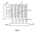
- FIG. 1 there is shown a very schematic view of the matrix sensor for producing a signal representing a thermal image taken by an infrared camera whose sensor is the sensitive element.
- the sensor comprises a matrix of lines and columns of pixels sensitive to infrared radiation.
- a pixel Pi, j at the intersection of a line of rank i and a column of rank j, is connected to at least one line conductor Li connecting all the pixels of this line and is connectable to a column conductor Cj connecting all the pixels of this column.
- the line conductor Li serves for the addressing of the pixel line; a line addressing circuit ADL successively addresses the different lines of the matrix and the addressing of a line of rank i causes the effective connection of each of the pixels of this line to the column driver corresponding to this pixel.
- a read circuit designated CLj for the rank column j, which can read a signal applied to the corresponding column driver Cj by the pixel of the addressed line.
- a multiplexer MUX receives the outputs of all the reading circuits CLj and makes it possible to rapidly supply on an output SV, signals coming from each of the reading circuits.
- the multiplexer MUX emits on the output SV a succession of signals, each signal corresponding to a respective column, in the order of the columns; this succession is transmitted at high speed so that all the signals which have been produced at the end of the addressing of a row of the matrix are sent on the output SV during the duration of addressing of the next line of the matrix .
- the figure 2 represents the elementary schematic diagram of an individual pixel Pi, j whose sensitive element is a bolometric element.
- the bolometric element is represented by a resistance Rb whose value varies as a function of its temperature and whose temperature varies in particular as a function of the integral of the infrared radiation flux received.
- the bolometric resistance Rb has a first end connected to a reference potential VR (common to all the pixels of the matrix) and a second end connected to the source of a transistor T1 whose gate receives a potential VG.
- the drain of the transistor T1 is connected by a switch K1 to the column conductor Cj.
- the switch K1 is controlled by the line conductor Li; it is he who establishes or interrupts the connection between the pixel Pi, j and the column driver Cj; the connection is established by closing the switch K1 when the line Li is addressed; it is interrupted by opening the switch K1 when the line is not addressed.
- the transistor T1 is conductive during the addressing of the line, because the potential of the column conductor Cj is then greater than the reference potential VR and the fact that the potential VG is chosen higher at least one value VT at the potential VR; VT is the threshold voltage of transistor T1 and is typically 0.6 volts.
- This current is taken from the column conductor Cj to which the resistor is connected via the transistor T1 and the switch K1.
- a compensation current lcomp is applied to the column conductor Cj at the column head, from a power source placed at the head of the column.
- the foot of the column is maintained, as will be seen, at a reference potential Vref.
- Vcomp a predetermined voltage
- Rcomp resistor
- the current Icomp can be produced by means other than the application of a given voltage to a resistance of given value: in particular, it can be fixed by a current source of known value lcomp.
- the column conductor Cj is connected to the measurement circuit CLj associated with the rank column j.
- This circuit will measure the residual current Id which runs through the column conductor towards the foot of the column.
- This residual current Id is the difference between the current Icomp and the measurement current Im which is taken by the pixel when it is connected to the column conductor.
- the read circuit CLj comprises a current integrator which will integrate the residual current for the duration T L reserved for this measurement for a line of pixels.
- the line Li is addressed for a duration slightly longer than the duration T L , before the addressing of the next line, but the integration will be made only over the duration T L ; for example the duration T L is 50 microseconds for a line addressing period of 64 microseconds.
- the duration T L is 50 microseconds for a line addressing period of 64 microseconds.
- the integrator comprises an operational amplifier AOP whose non-inverting input receives the reference potential Vref and whose inverting input is connected to the column Cj to receive the residual current Id.
- the capacitance Cint is connected between the inverting input and the output of the operational amplifier AOP.
- a switch K2 connected between the terminals of the capacitor makes it possible to short-circuit the integration capacitance Cint and thus zero the voltage across this capacitor at a zero reference instant defining the beginning of a new integration whose duration is T L.
- This switch K2 is thus briefly closed (for example for 4 microseconds) at the end of the addressing cycle of the preceding line (or at the beginning of the addressing cycle of the line Li) and it opens at the instant 0 defining for each line the start of a signal measurement period. By opening, it allows the beginning of the integration in the capacity.
- the output S of the amplifier is connected by a switch K3 to a storage capacitor Cst whose function is to memorize the value of the voltage VS after the end of the integration time and during the reading of the next line.
- the switch K3 is closed briefly (for example 1 microsecond) towards the end of the integration cycle, then reopened at the instant T L which marks the end of the integration time for a line.
- the voltage at the terminals of the storage capacitor Cst takes a value equal to the value reached at the instant T L by the voltage VS.
- the voltage at the terminals of the storage capacitor Cst is applied via a high impedance input buffer amplifier (to avoid a loss of charge of the capacitance) at a respective row-of-rank input of the multiplexer MUX. .
- the multiplexer can transmit a signal corresponding to this voltage at any time during the time interval reserved for reading the pixels coming from the line Li, that is to say during the time interval during which the next line of rank i + 1 is addressed.
- the compensation current Icomp is preferably chosen, acting on Vcomp and Rcomp, so that the residual current Id is zero at a reference temperature.
- This reference temperature is for example an ambient temperature of 300 ° K.
- VT is set by technology.
- VG and VR, as well as Icomp can be freely chosen.
- this ideal pixel will provide a VS voltage signal centered around Vref: greater than Vref when exposed to a temperature above 300 ° K and below Vref when exposed to a lower temperature.
- Rb is a quantity with high technological dispersion, and can have at the reference temperature values very different from the nominal value Rb0 for the different pixels of the matrix.
- the sensor architecture we are talking about here is a line-by-line addressing architecture: the pixel is powered by a current of polarization only during line addressing (typically less than 64 microseconds). This is why a relatively large bias current is provided in the resistor Rb at this time. The influence of this current is then considerable compared to the variations of this current generated by the exposure of the pixel to infrared radiation.
- the nominal value of the resistance varies by 15% because of the technological dispersions, whereas the resistance varies only by 1% according to the illumination received, between a minimum illumination and a maximum illumination. The obtaining on the sensor of an image having a real meaning with respect to the illumination received is therefore extremely disturbed by this dispersion.
- each pixel by means of an analog sensitivity adjustment circuit specific to this pixel, this adjustment circuit reacting to an adjustment voltage value stored on a capacitance. adjustment.
- This voltage value is provided by a feedback circuit receiving information from the measuring circuit at the bottom of the column and providing a charge to the pixel-specific adjustment capability; the adjustment value can be provided in particular (but not necessarily) during a calibration phase consisting of uniform illumination of the sensor matrix (preferably an illumination at the reference temperature, for example 300 ° K).
- a pixel Pi, j having a resistance Rbij0 at the reference temperature will make it possible to establish, by the feedback loop, a voltage on an adjustment capacity that is specific to it.
- the value of the voltage stored on this capacitor will be such that for illumination by a reference thermal flux (or temperature), the output of the measurement circuit at the bottom of the column has a predetermined value, the same for all the pixels.
- the feedback circuit is self-correcting and the voltage on the adjustment capacitance is gradually established so that all the pixels provide after a certain time the same measurement signal for the reference heat flow although their resistors Rbij0 are different from each other at the temperature generated by this flow.
- the pixel-specific adjustment circuit acts on one of the following parameters:
- VG Vref, T L , Icomp, preferably VG which defines the bias voltage of the bolometric resistance during the addressing of the line.
- the adjustment circuit with the adjustment capability that controls it is not necessarily localized in the pixel itself, but the embodiments in which the adjustment capability is located in the pixel are advantageous compared to those which would have an adjustment capacity located outside the pixel.
- the adjustment capacity specific to the pixel and located in the pixel is designated Ca.
- the adjustment circuit is simply constituted by the transistor T1 already present at the figure 2 ; it plays the role of an adjustment circuit because it is mounted as a follower and the voltage on its source follows directly, at a threshold voltage drop VT close, the voltage present on its gate.
- This gate voltage is now the adjustment voltage present on the adjustment capacitor Ca mounted between the gate of transistor T1 and a ground at zero potential.
- the gate-substrate capacitance of the transistor T1 may moreover be considered to be part of the Ca adjustment capacity.
- the adjustment voltage, or gate voltage VG of the follower transistor directly determines the polarization voltage of the bolometric resistance as explained previously:
- Vpol VG-VT-VR, VG is now an individually variable voltage for each pixel.
- the bolometric resistance Rb is connected between the source of the follower transistor and a point at the reference potential VR common to all the pixels.
- the threshold voltage VT of the transistor can be considered as identical for all the pixels.
- the feedback circuit which serves to establish an appropriate adjustment voltage on the capacitance Ca comprises a CQ charge incrementation circuit whose function is to add on the adjustment capacity, after the reading of a line , a quantity of charges signed all the more important that the sensitivity of the pixel is different from the nominal sensitivity desired for all the pixels.
- the quantity of charges is positive or negative and is added to the amount of charges previously stored on the adjustment capacity. The sign of the quantity of charges thus added is such that the sensitivity of the pixel tends to approach the desired nominal sensitivity.
- the incrementation circuit CQ uses, as a command, to determine the quantity of charges to be added or subtracted, the voltage level VS collected by the reading circuit CLj at the end of the reading of the line, therefore after the instant T L which defines the end of the reading. It is indeed this level which represents, for a given illumination, the sensitivity of the pixel.
- a level of adjustment voltage on capacitance Ca preferably very small increments are performed in the following manner: the voltage level VS which is stored in the storage capacitor Cst at the end of the reading of the line, is applied to a capacitance of larger size Cdiv preloaded at a medium voltage level which will be clarified later and will be called here Vgris. Vgris is preferably equal to Vref.
- the precharging is preferably performed during a short time interval at the end of the current integration time T L. During this time interval, a switch K5 connects the capacitance Cdiv to a voltage reference Vgris. The control of the switch K5 is in practice simultaneous with the command of the switch K3.
- a switch K4 serves to connect the capacitance Cst with the capacitance Cdiv. The switch K4 is closed briefly, and this closure can be performed only after the reopening of the switch K5.
- the role of the Cdiv capacitance is to constitute a kind of capacitive divider such that the voltage across the capacitance Cdiv, initially at Vgris because of the precharging, is incremented by a fraction of the difference between VS and Vgris. More precisely, the tension goes from Vgris to Vgris + VS - Vgris .
- the voltage across the capacitance Cdiv is then applied as a control voltage to the charge increment circuit CQ to change the load of the adjustment capacitor Ca in proportion to the difference (VS-Vgris) .Cst / (Cst + Cdiv), that is to say in proportion to the small incrementation or decrementation of tension which has just been made on the capacity Cdiv.
- the charge increment circuit is shown as being located geographically in each pixel. One can also consider an incrementation circuit common to all the pixels.
- the load variation of the capacitor Ca is of course made in a direction tending to reduce the sensitivity of the pixel to the desired nominal value.
- the sensitivity calibration of the pixel is therefore preferably done by measuring the analog voltage VS continuously and adding to the adjustment capacitance a small quantity of charges such that the adjustment circuit modifies the difference in voltage by a small percentage.
- VS-Vgris provided by the pixel for a given illumination Vgris being a reference voltage value corresponding to the analog voltage provided by a desired sensitivity pixel for medium illumination.
- a percentage less than 10% will be understood if the calibration is made in a specific calibration phase from a uniform illumination source, and a percentage less than or equal to 1% if the calibration is made during the calibration. use itself without a source of uniform illumination.
- the capacitance Cdiv must be connected to the circuit for incrementing charges of the pixel whose voltage VS has just been measured.
- the Cdiv capacitance can be connected to the pixel by a return driver Cr which is common to the entire column of pixels (column of rank j).
- the incrementing circuit CQ at the pixel Pi, j must perform a charge transfer on the capacitor Ca only while the conductor Cr carries voltage information relative to this pixel and not while carrying information relating to a measure on another pixel. This is why a switch K6 connects the input of the circuit CQ to the driver Cr, and this switch is closed only during the duration of addressing of a line, after which it is open.
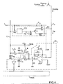
- the first hypothesis is used in the diagram of the figure 3 ; the second hypothesis is used in the schema of the figure 4 .
- the elements common with those of the figure 3 are designated by the same references.
- the link between the return conductor Cr and the pixel Pi, j is made by a switch K6 which is closed during the addressing of the line Li which corresponds to the pixel Pi, j and not by the addressing of the line Li + 1 which corresponds to the pixel Pi + 1, j.
- the capacitance Cst played a dual role of storing the voltage VS for the multiplexer and controlling the voltage level of the capacitance Cdiv, these two roles are now separated, the second role being attributed to the auxiliary capacitor C'st.
- the capacitor C'st can be charged to the voltage VS for a short time at the end of the duration T L thanks to a switch K7 connected between the output of the amplifier AOP and the capacitor C'st.
- the switch K7 is actuated at the same time as the switch K3 and the switch K5.
- the switch K4 is no longer connected between the capacitance Cst and the capacitance Cdiv but between the capacitor C'st and the capacitor Cdiv.
- the capacity Cst can then have a value much stronger than the capacity C'st.
- Cst is 1 picofarad and Cst is 0.1 picofarad in the scheme of the figure 4 , whereas Cst is rather 0.1 picofarad in the diagram of the figure 3 in order to fulfill both the main role of storing the pixel level in normal use, and the auxiliary role of developing the adjustment voltage on the return conductor Cr.
- the voltage Vgris is chosen as a function of the constitution of the charge incrementing circuit CQ. Indeed, the latter has the function of converting a voltage (VS-Vgris) .Cst / (Cst + Cdiv) into a quantity of charges dQ proportional to (VS-Vgris).
- this charge increment conversion circuit which performs a voltage / charge conversion, is symmetrically constituted and supplied between a low supply voltage at 0 volts and a high supply voltage at Vdd it is understood that it can easily perform a charge quantity creation proportional to VS-Vgris if Vgris is chosen equal to Vdd / 2.
- Vgris Vdd / 2 and the switch K5 will be connected to a voltage Vdd / 2 obtained for example by a resistive divider bridge placed between the potentials 0 and Vdd .
- the adjustment voltage can be used to control the value of the compensation current Icomp applied to the column conductor during the addressing of the line corresponding to the rank i of the pixel in question.
- the adjustment voltage it is possible to provide in the pixel a shunt to ground of a current controlled by the adjustment voltage obtained by the feedback circuit.
- the reference voltage Vref is modified by the feedback circuit, and this for each pixel. But it is understood that in this case the feedback circuit does not return to the pixel since the Vref voltage is not brought geographically into the pixel. This means that it is necessary to provide, outside the matrix of the actual sensor, a network of adjustment capabilities able to act on the reference voltage Vref in the same way as the adjustment capacity Ca of the figures 3 and 4 acts on the voltage Vpol.
- This network of adjustable capabilities is addressable along with the pixel lines to be able to match a specific adjustable capacity to a given pixel, both during a calibration operation and during normal use if these two operations are distinct.
- each pixel has an integration time adjusted so that the apparent sensitivity of the pixel for a reference illumination is the same for all the pixels.
- the signal level VS depends directly, as we have seen the integration time T L.
- a calibration phase with a reference thermal luminance screen is not mandatory and that the calibration can simply consist in allowing the adjustment voltage to gradually take on a stable value corresponding to the same value. average sensitivity for all pixels.
- the recursive method indicated above by which a small signed charge increment is added to the adjustment capacity when the pixel provides a signal different from the average reference Vgris, leads in fact gradually to a stabilization of all the pixels around the pixel. an average sensitivity since it is considered that, on a large number of images, all the pixels must see the same statistical distribution of thermal luminances.
- the time constant must be very large (several hundreds of images, that is to say at least several seconds) and therefore the capacitive division ratio Cst / (Cst + Cdiv) or C'st / (C'st + Cdiv) must be very small (preferably less than or equal to 0.01). This is in fact the condition for each new illumination of a pixel to modify very little the VG adjustment voltage stored on the capacitor Ca.
- a mixed mode that is to say an initial calibration phase with exposure of the whole matrix to a uniform heat flow followed by a phase of use with permanent self-correction
- the calibration mode by exposure to a reference uniform thermal flux is the only one used (with a time constant of rather short duration (less than one second, ie a few tens of images), then means must be provided (no represented on figures 3 and 4 ) to allow the operation of the feedback loop in the calibration phase and then prohibit it during the use phase.
- the adjustment voltage developed during the calibration phase is maintained on the capacity Ca during the use phase until a new calibration phase.
Landscapes
- Engineering & Computer Science (AREA)
- Multimedia (AREA)
- Signal Processing (AREA)
- Physics & Mathematics (AREA)
- General Physics & Mathematics (AREA)
- Spectroscopy & Molecular Physics (AREA)
- Transforming Light Signals Into Electric Signals (AREA)
- Photometry And Measurement Of Optical Pulse Characteristics (AREA)
- Solid State Image Pick-Up Elements (AREA)
Claims (13)
- Thermischer Bildmatrixsensor, der Folgendes umfasst: eine Zeilen- und Spaltenmatrix von Pixeln, die zeilenweise adressierbar sind, und eine Reihe von Signalleseschaltungen (CLj), die jeweils einer Pixelspalte zugeordnet sind, um nacheinander, mit fortschreitender Adressierung der Zeilen, einen von einem Pixel (Pi,j) der Spalte ausgehenden Strom zu empfangen, wobei jedes Pixel der Matrix einen bolometrischen Widerstand hat, dessen Wert Rb von dem vom Pixel empfangenen Wärmefluss abhängig ist, wobei dieser Widerstand durch eine Polarisationsspannung mit dem Wert Vpol polarisiert ist, wobei die Leseschaltung einen Integrator zum Integrieren der Differenz zwischen dem durch den bolometrischen Widerstand fließenden Strom Vpol/Rb und einem Kompensationsstrom in einem Integrationskondensator umfasst, wobei der Sensor dadurch gekennzeichnet ist, dass er für jede Spalte der Matrix Folgendes umfasst: eine Rückkopplungsschleife (K4, Cdiv, Cr, K6, CQ), die vom Integrationskondensator der den Pixeln der Spalte gemeinsamen Leseschaltung zu einem für jedes Pixel spezifischen und in dem Pixel befindlichen Justagekondensator (Ca) verläuft, um in diesem Justagekondensator eine dem Pixel eigene Justagespannung (VG) zu speichern, und eine analoge Empfindlichkeitsjustageschaltung (T1), die sich in dem Pixel befindet und als Reaktion auf diese Justagespannung wirksam wird, um beim Lesen der Zeile, zu der das Pixel gehört, die Polarisationsspannung des bolometrischen Widerstands zu verändern, wobei die Rückkopplungsschleife einen Speicherkondensator (Cs, C'st) umfasst, um die von der Leseschaltung (CLj) angelegte Analogspannung VS zu speichern, einen den Pixeln der betrachteten Spalte (Cdiv) gemeinsamen Referenzkondensator, Mittel zum Vorladen dieses Referenzkondensators auf einen vorbestimmten Referenzspannungswert (Vgris), Mittel zum Hinzufügen einer Ladung zu diesem Referenzkondensator, die für die Differenz zwischen dieser vorbestimmten Spannung und der von der Leseschaltung angelegten Analogspannung (VS) repräsentativ ist, und Mittel (CQ) zum Hinzufügen einer Ladungsmenge zu dem Justagekondensator, die in Abhängigkeit von der Analogspannung an den Anschlüssen des Referenzkondensators bestimmt wird.
- Thermischer Bildmatrixsensor nach Anspruch 1, dadurch gekennzeichnet, dass die Empfindlichkeitsjustageschaltung einen Spannungsfolgetransistor (T1) umfasst, dessen Source mit dem bolometrischen Widerstand verbunden ist und dessen Gate mit dem Justagekondensator verbunden ist.
- Thermischer Bildmatrixsensor nach Anspruch 2, dadurch gekennzeichnet, dass der bolometrische Widerstand zwischen der Source des Transistors und einem festen Potential (VR) geschaltet ist, das allen Pixeln der Matrix gemeinsam ist.
- Thermischer Bildmatrixsensor nach Anspruch 2 oder 3, dadurch gekennzeichnet, dass der Drain des Transistors über einen Zeilenadressierschalter mit einem Spaltenleiter (Cr) verbunden ist, zu dem der Kompoensationsstrom (Icomp) gespeist wird.
- Thermischer Bildmatrixsensor nach einem der Ansprüche 1 bis 4, dadurch gekennzeichnet, dass sich der Referenzkondensator (Cdiv) am Fuß der Spalte befindet und über einen Rückführungsleiter (Cr) mit den Pixeln der Spalte verbunden ist.
- Thermischer Bildmatrixsensor nach einem der Ansprüche 1 bis 5, dadurch gekennzeichnet, dass der Speicherkondensator ein Hauptspeicherkondensator (Cst) ist, der zum Festhalten einer Signalinformation VS nach dem Lesen einer Zeile und vor dem Adressieren einer Folgezeile dient.
- Thermischer Bildmatrixsensor nach einem der Ansprüche 1 bis 6, dadurch gekennzeichnet, dass der Speicherkondensator ein Zusatzkondensator (C'st) zum Aufnehmen einer Spannung ist, die mit der identisch ist, die an einen Hauptspeicherkondensator zum Halten einer Signalinformation VS nach dem Lesen einer Zeile und beim Adressieren einer Folgezeile angelegt wird.
- Thermischer Bildmatrixsensor nach einem der Ansprüche 1 bis 7, dadurch gekennzeichnet, dass er Mittel umfasst, um die Funktion der Rückkopplungsschaltung in einer Kalibrierphase zuzulassen und in einer Nutzphase nach einer Kalibrierphase zu sperren.
- Thermischer Bildmatrixsensor nach einem der Ansprüche 1 bis 8, dadurch gekennzeichnet, dass die Mittel (CQ) zum Hinzufügen einer bestimmten Ladungsmenge so ausgelegt sind, dass sie in der Nutzphase die Spannung des Justagekondensators um einen Anteil von weniger als 10% der Differenz zwischen der Ausgangsspannung VS der Leseschaltung und einer Referenzspannung (Vgris) verändert, die eine gewünschte Empfindlichkeit des Pixels für eine mittlere Lichtintensität so definiert, dass sich die Spannung des Justagekondensators langsam auf einem Wert stabilisiert, bei dem das Pixel die Referenzspannung für eine Lichtintensität liefert, die der Mittelwert der im Laufe der Nutzung empfangenen Lichtintensitäten ist.
- Verfahren zum Reduzieren von festem räumlichem Rauschen in einem thermischen Bildmatrixsensor nach Anspruch 1, wobei das Verfahren gekennzeichnet ist durch:- Messen der von einem Pixel ausgegebenen Analogspannung VS,- Hinzufügen einer bestimmten, vom Pegel der gemessenen Spannung abhängigen Ladungsmenge zu dem für das Pixel spezifischen und in dem Pixel befindlichen Justagekondensator (Ca),- Steuern, auf der Basis der im Justagekondensator gespeicherten Spannung, der Justageschaltung in dem Pixel, die beim Lesen der Zeile, zu der das Pixel gehört, auf die Polarisationsspannung Vpol wirkt.
- Verfahren nach Anspruch 10, dadurch gekennzeichnet, dass die Analogspannung VS im Laufe der Kalibrierphase gemessen wird, während der die Matrix mit einer gleichmäßigen Referenzlichtintensität beleuchtet wird.
- Verfahren nach Anspruch 11, dadurch gekennzeichnet, dass die Analogspannung VS zyklisch während der Kalibrierphase gemessen wird und die dem Justagekondensator hinzugefügte Ladungsmenge eine so geringe Ladungsmenge ist, dass die Justageschaltung die von dem Pixel für eine gegebene Lichtintensität gelieferte Spannungsdifferenz VS-Vgris um einen Anteil von weniger als 10% verändert, wobei Vgris ein Referenzspannungswert ist, der der Analogspannung entspricht, die von einem Pixel mit der gewünschten Empfindlichkeit für die Referenzlichtintensität geliefert wird.
- Verfahren nach einem der Ansprüche 10 bis 12, dadurch gekennzeichnet, dass die Analogspannung VS zyklisch während der normalen Nutzung des Sensors gemessen wird und die dem Justagekondensator hinzugefügte Ladungsmenge eine so geringe Ladungsmenge ist, dass die Justageschaltung die von dem Pixel für eine gegebene Lichtintensität gelieferte Spannungsdifferenz VS-Vgris um einen Anteil von weniger als 1% verändert, wobei Vgris ein Referenzspannungswert ist, der der Analogspannung entspricht, die von einem Pixel mit der gewünchten Empfindlichkeit für eine mittlere Lichtintensität geliefert wird.
Applications Claiming Priority (1)
| Application Number | Priority Date | Filing Date | Title |
|---|---|---|---|
| FR0707418A FR2922683B1 (fr) | 2007-10-23 | 2007-10-23 | Capteur d'image thermique matriciel a pixel bolometrique et procede de reduction de bruit spatial. |
Publications (2)
| Publication Number | Publication Date |
|---|---|
| EP2059030A1 EP2059030A1 (de) | 2009-05-13 |
| EP2059030B1 true EP2059030B1 (de) | 2011-01-19 |
Family
ID=39365778
Family Applications (1)
| Application Number | Title | Priority Date | Filing Date |
|---|---|---|---|
| EP08167221A Not-in-force EP2059030B1 (de) | 2007-10-23 | 2008-10-22 | Thermischer Matrixbildsensor mit bolometrischen Pixeln und Verfahren zur Reduzierung von speziellen Geräuschen |
Country Status (8)
| Country | Link |
|---|---|
| US (1) | US20090121139A1 (de) |
| EP (1) | EP2059030B1 (de) |
| JP (1) | JP2009103700A (de) |
| CN (1) | CN101419094A (de) |
| AT (1) | ATE496484T1 (de) |
| CA (1) | CA2641376A1 (de) |
| DE (1) | DE602008004611D1 (de) |
| FR (1) | FR2922683B1 (de) |
Families Citing this family (22)
| Publication number | Priority date | Publication date | Assignee | Title |
|---|---|---|---|---|
| FR2920872B1 (fr) * | 2007-09-10 | 2009-11-06 | Centre Nat Rech Scient | Bolometre a asservissement de chaleur. |
| FR2946743B1 (fr) * | 2009-06-15 | 2012-01-27 | Commissariat Energie Atomique | Dispositif de detection de rayonnements electromagnetiques a detecteur bolometrique polarise, application a une detection infrarouge |
| FR2959013B1 (fr) * | 2010-04-16 | 2012-05-11 | Commissariat Energie Atomique | Dispositif de detection de rayonnement electromagnetique a sensibilite reduite au bruit spacial |
| FR2968078A1 (fr) * | 2010-11-29 | 2012-06-01 | Commissariat Energie Atomique | Circuit électronique de polarisation et de lecture de détecteur thermique résistif |
| FR2972851B1 (fr) | 2011-03-18 | 2013-12-20 | Commissariat Energie Atomique | Capteur d'images |
| CN103335717B (zh) * | 2013-06-21 | 2015-11-18 | 中国科学院西安光学精密机械研究所 | 一种基于变积分模式的红外热像仪高精度抗温漂测温方法 |
| CN103335716B (zh) * | 2013-06-21 | 2016-06-08 | 中国科学院西安光学精密机械研究所 | 基于变积分时间的面阵红外相机定标与非均匀性校正方法 |
| FR3009388B1 (fr) * | 2013-07-30 | 2015-07-17 | Ulis | Diagnostic de l'etat defectueux d'une matrice de detection bolometrique |
| US9410850B2 (en) * | 2013-09-20 | 2016-08-09 | Vlad Joseph Novotny | Infrared imager readout electronics |
| FR3015770B1 (fr) * | 2013-12-19 | 2016-01-22 | Commissariat Energie Atomique | Procede et systeme de controle de qualite de cellules photovoltaiques |
| JP6213668B2 (ja) * | 2014-04-22 | 2017-10-18 | 日本電気株式会社 | 半導体装置と該半導体装置を備えた赤外線撮像装置、及び半導体装置の制御方法 |
| US11108975B2 (en) | 2017-04-11 | 2021-08-31 | Mikrosens Elektronik San. Ve Tic. | On-chip bias calibration for microbolometer detectors and readout integrated circuits |
| JP6874578B2 (ja) * | 2017-07-26 | 2021-05-19 | 富士通株式会社 | アレイセンサおよび撮像装置 |
| EP3841739A1 (de) | 2018-08-23 | 2021-06-30 | Raytheon Company | Vorspannungssteuerung eines propixeldetektors |
| TWI705235B (zh) * | 2019-07-19 | 2020-09-21 | 財團法人工業技術研究院 | 感測裝置 |
| FR3105444B1 (fr) * | 2019-12-24 | 2022-01-07 | Commissariat Energie Atomique | Procédé de détermination d'un biais affectant des pixels d'un détecteur pixellisé de rayonnement ionisant |
| US11561132B2 (en) | 2020-06-04 | 2023-01-24 | Raytheon Company | Per-pixel detector bias control |
| CN112214953B (zh) * | 2020-10-20 | 2022-08-05 | 中国科学院新疆理化技术研究所 | 一种电路级总剂量辐射效应仿真方法 |
| US12455193B2 (en) * | 2021-08-25 | 2025-10-28 | Flir Systems Ab | Variable sensitivity in infrared imaging systems and methods |
| CN114878033B (zh) * | 2022-03-29 | 2023-12-22 | 深圳国微感知技术有限公司 | 一种矩阵式压力分布测量系统及方法 |
| WO2024167995A1 (en) * | 2023-02-07 | 2024-08-15 | Owl Autonomous Imaging, Inc. | Methods and systems for thermal image sensing |
| TWI866362B (zh) * | 2023-07-28 | 2024-12-11 | 高爾科技股份有限公司 | 熱影像陣列像素動態校正之方法 |
Family Cites Families (3)
| Publication number | Priority date | Publication date | Assignee | Title |
|---|---|---|---|---|
| US5756999A (en) * | 1997-02-11 | 1998-05-26 | Indigo Systems Corporation | Methods and circuitry for correcting temperature-induced errors in microbolometer focal plane array |
| US6953932B2 (en) * | 1999-10-07 | 2005-10-11 | Infrared Solutions, Inc. | Microbolometer focal plane array with temperature compensated bias |
| FR2848666B1 (fr) * | 2002-12-16 | 2005-01-21 | Fr De Detecteurs Infrarouges S | Dispositif de detection de rayonnements electromagnetiques |
-
2007
- 2007-10-23 FR FR0707418A patent/FR2922683B1/fr not_active Expired - Fee Related
-
2008
- 2008-10-17 US US12/253,507 patent/US20090121139A1/en not_active Abandoned
- 2008-10-21 CA CA002641376A patent/CA2641376A1/en not_active Abandoned
- 2008-10-21 JP JP2008270790A patent/JP2009103700A/ja active Pending
- 2008-10-22 AT AT08167221T patent/ATE496484T1/de not_active IP Right Cessation
- 2008-10-22 EP EP08167221A patent/EP2059030B1/de not_active Not-in-force
- 2008-10-22 DE DE602008004611T patent/DE602008004611D1/de active Active
- 2008-10-23 CN CNA2008101708784A patent/CN101419094A/zh active Pending
Also Published As
| Publication number | Publication date |
|---|---|
| ATE496484T1 (de) | 2011-02-15 |
| CN101419094A (zh) | 2009-04-29 |
| FR2922683B1 (fr) | 2010-09-17 |
| EP2059030A1 (de) | 2009-05-13 |
| CA2641376A1 (en) | 2009-04-23 |
| DE602008004611D1 (de) | 2011-03-03 |
| US20090121139A1 (en) | 2009-05-14 |
| FR2922683A1 (fr) | 2009-04-24 |
| JP2009103700A (ja) | 2009-05-14 |
Similar Documents
| Publication | Publication Date | Title |
|---|---|---|
| EP2059030B1 (de) | Thermischer Matrixbildsensor mit bolometrischen Pixeln und Verfahren zur Reduzierung von speziellen Geräuschen | |
| EP2356810B1 (de) | Bildaufnehmer mit doppelter ladungsträgerübertragung für hohen dynamikumfang und das entsprechende steuerungsverfahren | |
| CA2726821C (fr) | Dispositif et procede de detection d'un rayonnement infrarouge au moyen d'une matrice de bolometres resistifs | |
| FR2869999A1 (fr) | Dispositif a auto-etalonnage pour la mesure de tension, et procede pour cela | |
| EP2770312A1 (de) | Bolometrischer Detektor mit temperaturabhängiger, kontrollierter Polarisation | |
| EP2177020B1 (de) | Verfahren zur empfindlichkeitskorrektur und matrixbildsensor zur implementierung dieses verfahrens | |
| EP3140906A1 (de) | Vorrichtung mit hohem dynamikumfang zur integration eines elektrischen stroms | |
| EP2687020A1 (de) | Blldsensor | |
| WO2010125281A1 (fr) | Systeme et procede de dectection de rayonnement infrarouge | |
| EP2622845B1 (de) | Bildgebungsvorrichtung mit ohmschem spannungsabfall von null bei einem datenleiter | |
| EP2833622B1 (de) | Diagnose des Störungszustands einer bolometrischen Erfassungsmatrix | |
| EP2383980A1 (de) | Bildsensor vom Typ CMOS mit einer ausgedehnten linearen Dynamik | |
| EP2894445A1 (de) | Vorrichtung und Verfahren zur Infrarot-Erkennung | |
| EP2132703B1 (de) | Verfahren zum korrigieren des space-rauschens eines bildsensors | |
| EP4216564B1 (de) | Kalibrierung eines digitalen iwr-pixels eines bildsensors | |
| EP0749234B1 (de) | Halbleiter-Bildsensor mit integrierte Pixelhistogrammumwandlung | |
| WO2016174036A1 (fr) | Capteur comprenant des pixels a detection capacitive | |
| EP2135220B1 (de) | Verfahren zur korrektur des räumlichen rauschens eines bildsensors mittels luminanzbegrenzung | |
| WO2020049460A1 (fr) | Dispositif imageur à grande vitesse d'acquisition et à gamme dynamique étendue | |
| WO2010136521A1 (fr) | Dispositif electronique d'ebasage du courant issu de detecteurs de rayonnement electromagnetique | |
| WO2011138738A1 (fr) | Appareil de mesure de la resistance electrique locale d'une surface | |
| WO2025088141A1 (fr) | Photodetecteur et capteur d'image photoelectrique a grande plage dynamique | |
| FR2932635A1 (fr) | Capteur d'image du type tdi a dynamique auto adaptee par point image | |
| WO1999035820A1 (fr) | Dispositif de prise de vue a transfert de charges sur un element de connexion |
Legal Events
| Date | Code | Title | Description |
|---|---|---|---|
| PUAI | Public reference made under article 153(3) epc to a published international application that has entered the european phase |
Free format text: ORIGINAL CODE: 0009012 |
|
| AK | Designated contracting states |
Kind code of ref document: A1 Designated state(s): AT BE BG CH CY CZ DE DK EE ES FI FR GB GR HR HU IE IS IT LI LT LU LV MC MT NL NO PL PT RO SE SI SK TR |
|
| AX | Request for extension of the european patent |
Extension state: AL BA MK RS |
|
| 17P | Request for examination filed |
Effective date: 20090929 |
|
| AKX | Designation fees paid |
Designated state(s): AT BE BG CH CY CZ DE DK EE ES FI FR GB GR HR HU IE IS IT LI LT LU LV MC MT NL NO PL PT RO SE SI SK TR |
|
| RAP1 | Party data changed (applicant data changed or rights of an application transferred) |
Owner name: COMMISSARIAT A L'ENERGIE ATOMIQUE ET AUX ENERGIES |
|
| GRAP | Despatch of communication of intention to grant a patent |
Free format text: ORIGINAL CODE: EPIDOSNIGR1 |
|
| GRAS | Grant fee paid |
Free format text: ORIGINAL CODE: EPIDOSNIGR3 |
|
| GRAA | (expected) grant |
Free format text: ORIGINAL CODE: 0009210 |
|
| RBV | Designated contracting states (corrected) |
Designated state(s): AT BE BG CH CY CZ DE DK EE ES FI GB GR HR HU IE IS IT LI LT LU LV MC MT NL NO PL PT RO SE SI SK TR |
|
| AK | Designated contracting states |
Kind code of ref document: B1 Designated state(s): AT BE BG CH CY CZ DE DK EE ES FI GB GR HR HU IE IS IT LI LT LU LV MC MT NL NO PL PT RO SE SI SK TR |
|
| REG | Reference to a national code |
Ref country code: GB Ref legal event code: FG4D Free format text: NOT ENGLISH |
|
| REG | Reference to a national code |
Ref country code: CH Ref legal event code: EP |
|
| REG | Reference to a national code |
Ref country code: IE Ref legal event code: FG4D Free format text: LANGUAGE OF EP DOCUMENT: FRENCH |
|
| REF | Corresponds to: |
Ref document number: 602008004611 Country of ref document: DE Date of ref document: 20110303 Kind code of ref document: P |
|
| REG | Reference to a national code |
Ref country code: DE Ref legal event code: R096 Ref document number: 602008004611 Country of ref document: DE Effective date: 20110303 |
|
| REG | Reference to a national code |
Ref country code: NL Ref legal event code: VDEP Effective date: 20110119 |
|
| LTIE | Lt: invalidation of european patent or patent extension |
Effective date: 20110119 |
|
| PG25 | Lapsed in a contracting state [announced via postgrant information from national office to epo] |
Ref country code: SE Free format text: LAPSE BECAUSE OF FAILURE TO SUBMIT A TRANSLATION OF THE DESCRIPTION OR TO PAY THE FEE WITHIN THE PRESCRIBED TIME-LIMIT Effective date: 20110119 Ref country code: NO Free format text: LAPSE BECAUSE OF FAILURE TO SUBMIT A TRANSLATION OF THE DESCRIPTION OR TO PAY THE FEE WITHIN THE PRESCRIBED TIME-LIMIT Effective date: 20110419 Ref country code: IS Free format text: LAPSE BECAUSE OF FAILURE TO SUBMIT A TRANSLATION OF THE DESCRIPTION OR TO PAY THE FEE WITHIN THE PRESCRIBED TIME-LIMIT Effective date: 20110519 Ref country code: PT Free format text: LAPSE BECAUSE OF FAILURE TO SUBMIT A TRANSLATION OF THE DESCRIPTION OR TO PAY THE FEE WITHIN THE PRESCRIBED TIME-LIMIT Effective date: 20110519 Ref country code: LV Free format text: LAPSE BECAUSE OF FAILURE TO SUBMIT A TRANSLATION OF THE DESCRIPTION OR TO PAY THE FEE WITHIN THE PRESCRIBED TIME-LIMIT Effective date: 20110119 Ref country code: HR Free format text: LAPSE BECAUSE OF FAILURE TO SUBMIT A TRANSLATION OF THE DESCRIPTION OR TO PAY THE FEE WITHIN THE PRESCRIBED TIME-LIMIT Effective date: 20110119 Ref country code: GR Free format text: LAPSE BECAUSE OF FAILURE TO SUBMIT A TRANSLATION OF THE DESCRIPTION OR TO PAY THE FEE WITHIN THE PRESCRIBED TIME-LIMIT Effective date: 20110420 Ref country code: LT Free format text: LAPSE BECAUSE OF FAILURE TO SUBMIT A TRANSLATION OF THE DESCRIPTION OR TO PAY THE FEE WITHIN THE PRESCRIBED TIME-LIMIT Effective date: 20110119 Ref country code: ES Free format text: LAPSE BECAUSE OF FAILURE TO SUBMIT A TRANSLATION OF THE DESCRIPTION OR TO PAY THE FEE WITHIN THE PRESCRIBED TIME-LIMIT Effective date: 20110430 |
|
| REG | Reference to a national code |
Ref country code: IE Ref legal event code: FD4D |
|
| PG25 | Lapsed in a contracting state [announced via postgrant information from national office to epo] |
Ref country code: NL Free format text: LAPSE BECAUSE OF FAILURE TO SUBMIT A TRANSLATION OF THE DESCRIPTION OR TO PAY THE FEE WITHIN THE PRESCRIBED TIME-LIMIT Effective date: 20110119 Ref country code: AT Free format text: LAPSE BECAUSE OF FAILURE TO SUBMIT A TRANSLATION OF THE DESCRIPTION OR TO PAY THE FEE WITHIN THE PRESCRIBED TIME-LIMIT Effective date: 20110119 Ref country code: SI Free format text: LAPSE BECAUSE OF FAILURE TO SUBMIT A TRANSLATION OF THE DESCRIPTION OR TO PAY THE FEE WITHIN THE PRESCRIBED TIME-LIMIT Effective date: 20110119 Ref country code: BG Free format text: LAPSE BECAUSE OF FAILURE TO SUBMIT A TRANSLATION OF THE DESCRIPTION OR TO PAY THE FEE WITHIN THE PRESCRIBED TIME-LIMIT Effective date: 20110419 Ref country code: CY Free format text: LAPSE BECAUSE OF FAILURE TO SUBMIT A TRANSLATION OF THE DESCRIPTION OR TO PAY THE FEE WITHIN THE PRESCRIBED TIME-LIMIT Effective date: 20110119 Ref country code: PL Free format text: LAPSE BECAUSE OF FAILURE TO SUBMIT A TRANSLATION OF THE DESCRIPTION OR TO PAY THE FEE WITHIN THE PRESCRIBED TIME-LIMIT Effective date: 20110119 Ref country code: FI Free format text: LAPSE BECAUSE OF FAILURE TO SUBMIT A TRANSLATION OF THE DESCRIPTION OR TO PAY THE FEE WITHIN THE PRESCRIBED TIME-LIMIT Effective date: 20110119 |
|
| PG25 | Lapsed in a contracting state [announced via postgrant information from national office to epo] |
Ref country code: EE Free format text: LAPSE BECAUSE OF FAILURE TO SUBMIT A TRANSLATION OF THE DESCRIPTION OR TO PAY THE FEE WITHIN THE PRESCRIBED TIME-LIMIT Effective date: 20110119 Ref country code: IE Free format text: LAPSE BECAUSE OF FAILURE TO SUBMIT A TRANSLATION OF THE DESCRIPTION OR TO PAY THE FEE WITHIN THE PRESCRIBED TIME-LIMIT Effective date: 20110119 Ref country code: DK Free format text: LAPSE BECAUSE OF FAILURE TO SUBMIT A TRANSLATION OF THE DESCRIPTION OR TO PAY THE FEE WITHIN THE PRESCRIBED TIME-LIMIT Effective date: 20110119 |
|
| PLBE | No opposition filed within time limit |
Free format text: ORIGINAL CODE: 0009261 |
|
| STAA | Information on the status of an ep patent application or granted ep patent |
Free format text: STATUS: NO OPPOSITION FILED WITHIN TIME LIMIT |
|
| PG25 | Lapsed in a contracting state [announced via postgrant information from national office to epo] |
Ref country code: CZ Free format text: LAPSE BECAUSE OF FAILURE TO SUBMIT A TRANSLATION OF THE DESCRIPTION OR TO PAY THE FEE WITHIN THE PRESCRIBED TIME-LIMIT Effective date: 20110119 Ref country code: RO Free format text: LAPSE BECAUSE OF FAILURE TO SUBMIT A TRANSLATION OF THE DESCRIPTION OR TO PAY THE FEE WITHIN THE PRESCRIBED TIME-LIMIT Effective date: 20110119 Ref country code: SK Free format text: LAPSE BECAUSE OF FAILURE TO SUBMIT A TRANSLATION OF THE DESCRIPTION OR TO PAY THE FEE WITHIN THE PRESCRIBED TIME-LIMIT Effective date: 20110119 |
|
| 26N | No opposition filed |
Effective date: 20111020 |
|
| PG25 | Lapsed in a contracting state [announced via postgrant information from national office to epo] |
Ref country code: IT Free format text: LAPSE BECAUSE OF FAILURE TO SUBMIT A TRANSLATION OF THE DESCRIPTION OR TO PAY THE FEE WITHIN THE PRESCRIBED TIME-LIMIT Effective date: 20110119 |
|
| REG | Reference to a national code |
Ref country code: DE Ref legal event code: R097 Ref document number: 602008004611 Country of ref document: DE Effective date: 20111020 |
|
| BERE | Be: lapsed |
Owner name: COMMISSARIAT A L'ENERGIE ATOMIQUE ET AUX ENERGIES Effective date: 20111031 |
|
| PG25 | Lapsed in a contracting state [announced via postgrant information from national office to epo] |
Ref country code: MC Free format text: LAPSE BECAUSE OF NON-PAYMENT OF DUE FEES Effective date: 20111031 |
|
| PG25 | Lapsed in a contracting state [announced via postgrant information from national office to epo] |
Ref country code: BE Free format text: LAPSE BECAUSE OF NON-PAYMENT OF DUE FEES Effective date: 20111031 Ref country code: DE Free format text: LAPSE BECAUSE OF NON-PAYMENT OF DUE FEES Effective date: 20120501 |
|
| REG | Reference to a national code |
Ref country code: DE Ref legal event code: R119 Ref document number: 602008004611 Country of ref document: DE Effective date: 20120501 |
|
| REG | Reference to a national code |
Ref country code: AT Ref legal event code: MK05 Ref document number: 496484 Country of ref document: AT Kind code of ref document: T Effective date: 20110119 |
|
| PG25 | Lapsed in a contracting state [announced via postgrant information from national office to epo] |
Ref country code: MT Free format text: LAPSE BECAUSE OF FAILURE TO SUBMIT A TRANSLATION OF THE DESCRIPTION OR TO PAY THE FEE WITHIN THE PRESCRIBED TIME-LIMIT Effective date: 20110119 |
|
| PG25 | Lapsed in a contracting state [announced via postgrant information from national office to epo] |
Ref country code: LU Free format text: LAPSE BECAUSE OF NON-PAYMENT OF DUE FEES Effective date: 20111022 |
|
| REG | Reference to a national code |
Ref country code: CH Ref legal event code: PL |
|
| GBPC | Gb: european patent ceased through non-payment of renewal fee |
Effective date: 20121022 |
|
| PG25 | Lapsed in a contracting state [announced via postgrant information from national office to epo] |
Ref country code: GB Free format text: LAPSE BECAUSE OF NON-PAYMENT OF DUE FEES Effective date: 20121022 Ref country code: LI Free format text: LAPSE BECAUSE OF NON-PAYMENT OF DUE FEES Effective date: 20121031 Ref country code: CH Free format text: LAPSE BECAUSE OF NON-PAYMENT OF DUE FEES Effective date: 20121031 |
|
| PG25 | Lapsed in a contracting state [announced via postgrant information from national office to epo] |
Ref country code: TR Free format text: LAPSE BECAUSE OF FAILURE TO SUBMIT A TRANSLATION OF THE DESCRIPTION OR TO PAY THE FEE WITHIN THE PRESCRIBED TIME-LIMIT Effective date: 20110119 |
|
| PG25 | Lapsed in a contracting state [announced via postgrant information from national office to epo] |
Ref country code: HU Free format text: LAPSE BECAUSE OF FAILURE TO SUBMIT A TRANSLATION OF THE DESCRIPTION OR TO PAY THE FEE WITHIN THE PRESCRIBED TIME-LIMIT Effective date: 20110119 |