EP2061177A1 - Circuit de reproduction de données - Google Patents
Circuit de reproduction de données Download PDFInfo
- Publication number
- EP2061177A1 EP2061177A1 EP06797356A EP06797356A EP2061177A1 EP 2061177 A1 EP2061177 A1 EP 2061177A1 EP 06797356 A EP06797356 A EP 06797356A EP 06797356 A EP06797356 A EP 06797356A EP 2061177 A1 EP2061177 A1 EP 2061177A1
- Authority
- EP
- European Patent Office
- Prior art keywords
- phase
- data
- synchronization
- continuous clock
- input
- Prior art date
- Legal status (The legal status is an assumption and is not a legal conclusion. Google has not performed a legal analysis and makes no representation as to the accuracy of the status listed.)
- Withdrawn
Links
Images





Classifications
-
- H—ELECTRICITY
- H04—ELECTRIC COMMUNICATION TECHNIQUE
- H04L—TRANSMISSION OF DIGITAL INFORMATION, e.g. TELEGRAPHIC COMMUNICATION
- H04L7/00—Arrangements for synchronising receiver with transmitter
-
- H—ELECTRICITY
- H04—ELECTRIC COMMUNICATION TECHNIQUE
- H04L—TRANSMISSION OF DIGITAL INFORMATION, e.g. TELEGRAPHIC COMMUNICATION
- H04L7/00—Arrangements for synchronising receiver with transmitter
- H04L7/02—Speed or phase control by the received code signals, the signals containing no special synchronisation information
- H04L7/033—Speed or phase control by the received code signals, the signals containing no special synchronisation information using the transitions of the received signal to control the phase of the synchronising-signal-generating means, e.g. using a phase-locked loop
- H04L7/0337—Selecting between two or more discretely delayed clocks or selecting between two or more discretely delayed received code signals
- H04L7/0338—Selecting between two or more discretely delayed clocks or selecting between two or more discretely delayed received code signals the correction of the phase error being performed by a feed forward loop
-
- H—ELECTRICITY
- H04—ELECTRIC COMMUNICATION TECHNIQUE
- H04L—TRANSMISSION OF DIGITAL INFORMATION, e.g. TELEGRAPHIC COMMUNICATION
- H04L12/00—Data switching networks
- H04L12/28—Data switching networks characterised by path configuration, e.g. LAN [Local Area Networks] or WAN [Wide Area Networks]
-
- H—ELECTRICITY
- H04—ELECTRIC COMMUNICATION TECHNIQUE
- H04L—TRANSMISSION OF DIGITAL INFORMATION, e.g. TELEGRAPHIC COMMUNICATION
- H04L7/00—Arrangements for synchronising receiver with transmitter
- H04L7/04—Speed or phase control by synchronisation signals
Definitions
- the present invention relates to a data recovery circuit for extracting, from input data, a clock synchronized in phase with the input data to reproduce the clock and discriminating and reproducing the input data based on the reproduced clock.
- Non-Patent Document 1 a passive optical networks (PON) system in which a parent station device (optical line terminal (OLT)) is connected to subscriber devices (optical network units (ONUs)) through an optical fiber.
- OLT optical line terminal
- ONUs optical network units
- the system structure is internationally standardized in, for example, Non-Patent Document 1.
- a time division multiplexing (TDM) method of performing temporal multiplexing is applied as a method of receiving light signals from the respective subscriber devices (ONUs). Therefore, a common system capable of containing the plurality of subscriber devices (ONUs) can be constructed using a single-core optical fiber transmission line, and hence the broadband access network can be economically constructed.
- TDM time division multiplexing
- the temporally multiplexed signals are burst light signals obtained by intermittently emitting/interrupting the light signals, and hence technical problems specific to input burst light signals occur in the parent station device (OLT) which is a receiver device.
- OLT parent station device
- a normal optical receiver provided in the parent station device includes an optical preamplifier for converting an input burst light signal into an electrical signal (input data) having a discriminable amplitude, and a data reproducing (clock and data recovery (CDR)) circuit for extracting a clock component from the input data and performing data recovery based on phase synchronization information.
- a phased lock loop (PLL) circuit using a continuous voltage controlled oscillator is normally used as a clock extraction system in the data recovery circuit.
- a control signal substantially close to a DC component is applied as a control signal for frequency and phase control. This is used to suppress fluctuation components (jitters) generated from the oscillator and the PLL. Accordingly, it is essentially difficult for a feedback-controlled clock extraction circuit such as the PLL to obtain high-speed response characteristics.
- the burst light signals in the PON system described above include light signals output from the plurality of subscriber devices (ONUs) with different transmission distances, and hence the respective burst light signals have various different reception phases.
- the frequencies of the burst light signals are synchronized with frequencies output from the respective subscriber devices (ONUs), and thus have a relative frequency deviation. Therefore, the data recovery circuit in the parent station device (OLT) is required to have a function for performing clock extraction and data recovery based on phase synchronization for each of the burst light signals at high speed.
- OLT parent station device
- a data recovery circuit for extracting a clock from the burst light signal at high speed has been proposed (see, for example, Patent Document 1).
- the conventional data recovery circuit generates, from received data, a gating signal synchronized with a rising phase or falling phase of input data.
- a toggle flip-flop whose output logic is reversed at a rising or falling edge of the input data is applied as a gating signal generating means.
- a gated oscillator which performs oscillation outputting or stopping in instant synchronization with the gating signal is provided, and hence the clock synchronized with the rising phase or falling phase of the input data is generated.
- outputs of two gated oscillators which perform oscillation outputting or stopping based on the positive logic and negative logic of the gating signal are combined in an OR gate, and hence clocks instantly synchronized in phase with the input data can be successively generated.
- the conventional data recovery circuit provides a high-speed clock extraction means even when phase information included in data input from the respective subscriber devices (ONUs) are uneven and temporally intermittent burst light signals are input.
- FIGS. 8A and 8B illustrate operations of the conventional data recovery circuit in a case where the jitter component is not included in the input data and in a case where the jitter component is superimposed thereon.
- a discrimination phase point for an extraction block is normally set based on a fixed delay time period, when an error of a phase of the extraction clock is caused by a jitter component, a problem occurs in which discrimination cannot be performed at an optimum phase clock in the conventional data recovery circuit. In the worst case, discrimination cannot be performed.
- an object of the present invention is to obtain a data recovery circuit capable of reproducing data discriminated from input data in an optimum discrimination phase at high speed and outputting data synchronized with a reference clock, even when a jitter component is superimposed on an input temporally intermittent burst light signal from a subscriber device (ONU).
- a data recovery circuit includes: an input data phase detection circuit for extracting, as a gate signal, a signal synchronized with input data from the input data and outputting the gate signal; a gated N-phase oscillator for generating N-phase clocks obtained by dividing a bit width of the input data into N in phase synchronization with the gate signal output from the input data phase detection circuit; N data discriminating and reproducing circuits for sampling the input data based on the N-phase clocks output from the gated N-phase oscillator and outputting sampled data; a continuous clock generation circuit for generating a continuous clock which is a reference clock; N continuous clock synchronization circuits for synchronizing the sampled data output from the N data discriminating and reproducing circuits with the continuous clock output from the continuous clock generation circuit and outputting the synchronized sampled data as phase synchronization data; and a phase selector for selecting, from the phase synchronization data output from the N continuous clock synchronization circuits, phase synchronization data having an optimum discrimination phase with
- the data recovery circuit in the present invention an effect is obtained in which even when the jitter component is superimposed on the input temporally intermittent burst light signal from the subscriber device (ONU), the data discriminated from the input data in the optimum discrimination phase at high speed can be reproduced and the data synchronized with the reference clock can be output.
- the present invention relates to a PON system.
- a parent station device OLT
- ONU subscriber device
- An optical receiver is provided in the parent station device (OLT).
- the optical receiver includes an optical preamplifier and a data recovery circuit.
- Embodiments 1 to 3 of the present invention relate to the data recovery circuit, and more particularly, to a data recovery circuit for extracting a clock at high speed and reproducing and extracting received data at a clock with an optimum phase for a retiming of the received data, even when a jitter component is superimposed on an input signal waveform of a temporally intermittent burst light signal from a subscriber device (ONU).
- ONU subscriber device
- FIG. 1 is a block diagram illustrating a structure of the data recovery circuit according to Embodiment 1 of the present invention.
- the same reference symbols indicate the same or corresponding portions.
- the data recovery circuit includes an input data phase detection circuit 1, a gated multiphase oscillator (N-phase gated voltage controlled oscillator (GVCO)) 2, N (natural number other than 1) data discriminating and reproducing circuits 3, a continuous clock generation circuit 4, N continuous clock synchronization circuits 5, and a phase selector 6.
- N-phase gated voltage controlled oscillator GVCO
- N natural number other than 1
- FIG. 2 is a timing chart illustrating operations of the input data phase detection circuit, the gated multiphase oscillator, and the data discriminating and reproducing circuit in the data recovery circuit according to Embodiment 1 of the present invention.
- FIG. 2 illustrates an operation from data input to data discrimination and recovery.
- circuit logic is described, and hence the influence of a timing deviation such as a circuit delay, which is caused in an actual circuit, is omitted. Specifically, a case where the number of phases N is 4 is described.
- the input data phase detection circuit 1 extracts, as a gate signal (b), a signal synchronized with input data (a) from the input data (a), and outputs the gate signal (b).
- the input data phase detection circuit 1 when the input data (a) is input from an optical preamplifier (not shown) provided at the preceding stage, as illustrated in FIG. 2 , the input data phase detection circuit 1 generates the gate signal (b) selectively synchronized with only a rising phase of the input data (a) (Note that the input data phase detection circuit 1 may generate the gate signal (b) selectively synchronized with only a falling phase of the input data (a)).
- the input data phase detection circuit 1 can be constructed using a normal logic circuit. For simple description, assume that an interval for which the gate signal (b) output here becomes logic L (Low) is shorter than a half period of clocks described later.
- the gated multiphase oscillator 2 generates N-phase (N phases) clocks (c) obtained by dividing a bit width BW of the input data (a) into N, in phase synchronization with the gate signal (b) output from the input data phase detection circuit 1.
- the gated multiphase oscillator 2 produces oscillation at the rising of the gate signal (b) as a trigger during an interval of logic H (High) of the gate signal (b).
- an interval of logic L of the gate signal (b) is shorter than the half period of the clocks described later, and hence the gated multiphase oscillator 2 does not stop oscillation and thus produces continuous oscillation while phase synchronization is reproduced again at a trigger point.
- the N data discriminating and reproducing circuits 3 sample the input data (a) based on the N-phase clocks (c) output from the gated multiphase oscillator 2 and output sampled data (d).
- the data discriminating and reproducing circuits 3 upon receiving the clocks (c) from the gated multiphase oscillator 2 as sampling clocks, the data discriminating and reproducing circuits 3 output the sampled data (d) which are synchronized with the respective phase clocks (c) and obtained by sampling the input data (a). The sampling is performed in synchronization with the rising edges of the respective phase clocks (c).
- FIG. 2 illustrates the case where the undefined data is logic L.
- the undefined state There is a state in which the input data (a) cannot be sampled in addition to the undefined state resulting from the overlap of both the edges. Such a state is also referred to as the undefined state. That is, herein, a state other than the state in which the sampling can be normally performed is referred to as the undefined state.
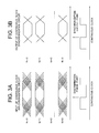
- FIGS. 3A and 3B illustrate an operation of a continuous clock synchronization circuit in the data recovery circuit according to Embodiment 1 of the present invention.
- FIGS. 3A and 3B illustrate an operation during which the sampled data (d) are input to the continuous clock synchronization circuits 5 and output as phase synchronization data (e).
- the N continuous clock synchronization circuits 5 synchronize the sampled data (d) output from the data discriminating and reproducing circuits 3 with a continuous clock output from the continuous clock generation circuit 4 and output the synchronized sampled data (d) as phase synchronization data (e).
- the continuous clock synchronization circuits 5 store the sampled data (d) in order.
- the continuous clock synchronization circuits 5 each includes, for example, a sequential storage device and can be easily realized using a normal first-in-first-out (FIFO) system.
- the sampled data (d) are output as data synchronized with the clocks (c) from the gatedmultiphase oscillator 2 and stored in the continuous clock synchronization circuits 5.
- the clocks (c) from the gated multiphase oscillator 2 are generated as clocks instantly synchronized in phase with the input data (a). Therefore, as illustrated in FIG. 3A , the clocks are input as the sampled data (d) on which jitter components depending on a fluctuation of the input data (a) are superimposed.
- the continuous clock synchronization circuits 5 synchronize the stored sampled data (d) with the continuous clock output from the continuous clock generation circuit 4 and output the synchronized sampled data as the phase synchronization data (e).
- the continuous clock generation circuit 4 is used as a reference clock generator of the entire optical receiver.
- the generated continuous clock includes no jitter component and thus is a clock whose phase is not changed. Therefore, the phase synchronization data (e) are output as data from which the jitter components are removed, and which are synchronized with the continuous clock, that is, the reference clock.
- the phase selector 6 selects the phase synchronization data (e) having an optimum discrimination phase with the largest phase margin with respect to the input data (a), from the phase synchronization data (e) output from the continuous clock synchronization circuits 5, and outputs the selected phase synchronization data as recovery data (f).
- the phase synchronization data (e) from which the jitter components are removed, and which are synchronized with the continuous clock (reference clock) are input to the phase selector 6.
- the phase selector 6 includes, for example, a logical table circuit and is set so as to select the phase synchronization data (e) in the phase having a maximum phase difference, from the phase of the phase synchronization data (e) which is undefined.
- the logical table circuit can be realized using a normal gate circuit and easily provided using a complementary metal oxide semiconductor (CMOS), a filed programable gate array (FPGA) or the like.
- CMOS complementary metal oxide semiconductor
- FPGA filed programable gate array
- a method of selecting the recovery data (f) with respect to the input data (a) can be arbitrarily realized.
- the phase selection operation for selecting the phase in which the phase difference from the undefined phase is maximum is executed in only one cycle (one time), it is likely to cause an error. Therefore, the phase selector 6 repeats the phase selection operation for a plurality of cycles to select the phase synchronization data (e) in a phase which is selected a largest number of times as a phase in which the phase difference is maximum, of the phases in which the phase difference is maximum.
- the phase selector 6 stores the N-phase phase synchronization data (e) output from the continuous clock synchronization circuits 5 for a predetermined time period (for example, 10 cycles), counts the phase, in which the phase difference from the undefined phase is maximum, for a predetermined time period for each phase, and selects the phase synchronization data (e) in the phase in which the count is largest.
- a predetermined time period for example, 10 cycles
- Embodiment 1 an effect of Embodiment 1 is described.
- bit width BW of the input data (a) is assumed to be 1 and an apparent bit width becomes 1 - dj because of a jitter component dj
- dp a phase margin of the data discriminating and reproducing circuit 3
- phase margin 270°
- an allowable jitter component dj becomes smaller than 0.25.
- the data recovery circuit according to Embodiment 1 samples the input data (a) based on the multiphase clocks. Therefore, even when the bit width becomes narrower because of the jitter component, it is sufficient that a clock edge corresponding to one phase which can be sampled during a bit window is input, and hence a condition for obtaining the recovery data (f) with no error can be expressed by the following Expression (2).
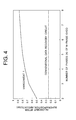
- FIG. 4 illustrates a relationship of the allowable jitter amount dj with respect to the number of phases N using Expressions (1) and (2) described above.
- the allowable jitter amount in the conventional data recovery circuit is 0.25 (UIpp)
- a jitter amount of up to 0.75 (UIpp) can be allowed in Embodiment 1 in the case where the number of phases N is 4.
- the data recovery circuit includes the input data phase detection circuit 1 for outputting the gate signal (b) synchronized with the rising or falling phase of the input data (a), the gated multiphase oscillator 2 for instantly generating the N-phase clocks (c) having phase differences in order based on the gate signal (b) as the trigger, the data discriminating and reproducing circuits 3 for outputting the sampled data (d) of the input data (a) which are synchronized with the clocks (c) based on the clocks (c) as the sampling clocks, the continuous clock generation circuit 4 for generating the continuous clock which is the reference clock, the continuous clock synchronization circuits 5 for synchronizing the stored sampled data (d) with the continuous clock and outputting the synchronized sampled data as the phase synchronization data (e), and the phase selector 6 for selecting the phase synchronization data (e) having the optimum discrimination phase with the largest phase margin with respect to the input data (a) and outputting the selected phase synchronization data as the recovery data (f
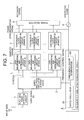
- FIG. 5 is a block diagram illustrating a structure of the data recovery circuit according to Embodiment 2 of the present invention.
- the data recovery circuit includes an input data phase detection circuit 1, a gated multiphase oscillator (N-phase GVCO) 2, N data discriminating and reproducing circuits 3, a continuous clock generation circuit 4, N continuous clock synchronization circuits 5, a phase selector 6, and an input pattern detection circuit 7.
- N-phase GVCO gated multiphase oscillator
- N data discriminating and reproducing circuits 3, a continuous clock generation circuit 4, N continuous clock synchronization circuits 5, a phase selector 6, and an input pattern detection circuit 7.
- Embodiment 2 is a modified example of Embodiment 1 described above.
- the sampling operation of the input data, the continuous clock synchronization operation, and the phase selection operation are similar to the operations of Embodiment 1, and thus the descriptions thereof are omitted.
- an input pattern detection operation of the input pattern detection circuit 7 is described.
- the input pattern detection circuit 7 When the input data (a) is input, the input pattern detection circuit 7 generates a logic H signal only when an input data pattern during an arbitrary time width (bit interval) is matched with a reference pattern held in advance in the input pattern detection circuit 7.
- the input pattern detection circuit 7 supplies the logic H signal as a reset signal to each of the N continuous clock synchronization circuits 5.
- the reference pattern is equal to a fixed bit pattern included in advance in the input data (a), that is, the input burst light signal.
- each of the N continuous clock synchronization circuits 5 The storage operation of each of the N continuous clock synchronization circuits 5 is controlled in response to the reset signal. Stored data are discarded and erased at the instant at which the reset signal is input, and the storage of the sampled data (d) is started again.
- the continuous clock synchronization circuits 5 each include, for example, a sequential storage device with reset signal. When the reset signal is input, the storage of the sampled data (d) is started by a first-in-first-out (FIFO) system.
- FIFO first-in-first-out
- FIGS. 6A, 6B and 6C illustrate states of stored data of the continuous clock synchronization circuit 5 during an interval ( ⁇ ) including an instant at which the burst light signal is input and during an interval ( ⁇ ) for which the burst light signal is stabilized at a constant value.
- distorted data are normally reproduced because of response characteristics of an optical preamplifier (not shown) or the like which is used at the preceding stage.
- clocks depending on the input data are generated, and hence data synchronized with distorted clocks are input. Therefore, as illustrated in FIGS.
- the stored data during the interval ( ⁇ ) immediately after the burst light signal is input includes an error, and thus stores erroneous operation signals.
- the fixed bit pattern set in advance is inserted to an arbitrary interval between the input data (a).
- the data recovery circuit includes the input data phase detection circuit 1, the gated multiphase oscillator 2, the data discriminating and reproducing circuits 3, the continuous clock generation circuit 4, the continuous clock synchronization circuits 5 which start the sequential storage operation of the sampled data when the reset signal is input, the phase selector 6, and the input pattern detection circuit 7 for outputting the reset signal only when the fixed bit pattern of the input data is matched with the reference pattern. Accordingly, even when the burst light signal is input and erroneous data is included during the interval ( ⁇ ) immediately after the input thereof, the data discriminated in the optimum discrimination phase can be reproduced from the input data at high speed and the data synchronized with the reference clock can be output.
- FIG. 7 is a block diagram illustrating a structure of the data recovery circuit according to Embodiment 3 of the present invention.
- the data recovery circuit includes an input data phase detection circuit 1, a gated multiphase oscillator (N-phase GVCO) 2, N data discriminating and reproducing circuits 3, a continuous clock generation circuit 4, N continuous clock synchronization circuits 5, a phase selector 6, and a frequency/phase synchronization circuit 8.
- N-phase GVCO gated multiphase oscillator
- N data discriminating and reproducing circuits 3, a continuous clock generation circuit 4, N continuous clock synchronization circuits 5, a phase selector 6, and a frequency/phase synchronization circuit 8.
- the frequency/phase synchronization circuit 8 includes a gated oscillator 81 and a frequency/phase comparator 82.
- Embodiment 3 is a modified example of Embodiment 1 described above.
- the sampling operation of the input data, the continuous clock synchronization operation, and the phase selection operation are similar to the operations of Embodiment 1, and thus the descriptions thereof are omitted.
- an operation of the frequency/phase synchronization circuit 8 is described.
- the gated oscillator 81 included in the frequency/phase synchronization circuit 8 has the same circuit structure as the gated multiphase oscillator 2 and is substantially equal in oscillation frequency to the gated multiphase oscillator 2.
- the frequency/phase comparator 82 included in the frequency/phase synchronization circuit 8 detects an error between a frequency/phase of a clock output from the gated oscillator 9 and a frequency/phase of the continuous clock generated by the continuous clock generation circuit 4 and outputs an error signal as a frequency control signal.
- the gated multiphase oscillator 2 includes, for example, a ring oscillation circuit.
- the ring oscillation circuit includes: a plurality of (N) delay elements whose delay amounts are arbitrarily controlled based on the frequency control signal; and a gating circuit for outputting AND results between outputs of the N delay elements and the gate signal (b).
- N outputs of the gating circuit correspond to N-phase clocks (c) with relative phase differences (delay differences).
- a gate signal of the gated oscillator 81 is logically fixed, thereby performing continuous oscillation.
- the gated oscillator 81 changes the oscillation frequency based on the frequency control signal to minimize the error signal from the frequency/phase comparator 82. Therefore, in a steady state, the output clock of the continuous clock generation circuit 4 which is the reference clock of the optical receiver is synchronized in frequency/phase with the output clock of the gated oscillator 81.
- the synchronization information is transferred as the frequency control signal to the gated multiphase oscillator 2.
- the oscillation frequency of the gated multiphase oscillator 2 is also controlled so as to be synchronized with the continuous clock.
- the oscillation frequency of the gated multiphase oscillator 2 is independently determined based on constants resulting from a self-circuit structure, and therefore includes a frequency deviation from the output clock of the continuous clock generation circuit 4 which is the reference clock of the optical receiver.
- the frequency deviation is large, an input data speed is not matched with an output data speed in the continuous clock synchronization circuits 5 serving as the sequential storage device, and hence a problem such as a storage overflow occurs.
- Even when the frequency deviation is suppressed by contriving circuit constants it is difficult to perform self-oscillation at a stable frequency for a change in ambient temperature or the like.
- the frequency/phase synchronization circuit 8 provided in Embodiment 3 is applied, it is possible to provide the stable gated multiphase oscillator 2 which is synchronized in phase with the input data at high speed and synchronized in frequency with the continuous clock generation circuit 4.
- the data recovery circuit includes the input data phase detection circuit 1, the gated multiphase oscillator 2 for generating the clocks synchronized with the continuous clock based on the frequency control signal, the N-phase data discriminating and reproducing circuits 3, the continuous clock generation circuit 4, the continuous clock synchronization circuits 5, the phase selector 6, and the frequency/phase synchronization circuit 8 for outputting, as the frequency control signal, the synchronization information of the continuous clock generated by the continuous clock generation circuit 4. Accordingly, even when the gated multiphase oscillator 2 includes the frequency deviation from the continuous clock of the continuous clock generation circuit 4, the data discriminated in the optimum discrimination phase can be reproduced from the input data with the stable frequency oscillation clock at high speed and the data synchronized with the reference clock can be output.
Landscapes
- Engineering & Computer Science (AREA)
- Computer Networks & Wireless Communication (AREA)
- Signal Processing (AREA)
- Synchronisation In Digital Transmission Systems (AREA)
- Optical Communication System (AREA)
Applications Claiming Priority (1)
| Application Number | Priority Date | Filing Date | Title |
|---|---|---|---|
| PCT/JP2006/317431 WO2008029438A1 (fr) | 2006-09-04 | 2006-09-04 | Circuit de reproduction de données |
Publications (2)
| Publication Number | Publication Date |
|---|---|
| EP2061177A1 true EP2061177A1 (fr) | 2009-05-20 |
| EP2061177A4 EP2061177A4 (fr) | 2011-05-18 |
Family
ID=39156883
Family Applications (1)
| Application Number | Title | Priority Date | Filing Date |
|---|---|---|---|
| EP06797356A Withdrawn EP2061177A4 (fr) | 2006-09-04 | 2006-09-04 | Circuit de reproduction de données |
Country Status (6)
| Country | Link |
|---|---|
| US (1) | US7924076B2 (fr) |
| EP (1) | EP2061177A4 (fr) |
| JP (1) | JP5068758B2 (fr) |
| KR (1) | KR101054638B1 (fr) |
| TW (1) | TW200814696A (fr) |
| WO (1) | WO2008029438A1 (fr) |
Cited By (2)
| Publication number | Priority date | Publication date | Assignee | Title |
|---|---|---|---|---|
| WO2013075009A3 (fr) * | 2011-11-16 | 2013-11-28 | Qualcomm Incorporated | Appareil et procédé de récupération de données à modulation de largeur d'impulsions en mode salve (pwm) et de non-retour à zéro (nrz) |
| CN112840593A (zh) * | 2018-12-21 | 2021-05-25 | 华为技术有限公司 | 一种跨时钟域处理电路 |
Families Citing this family (21)
| Publication number | Priority date | Publication date | Assignee | Title |
|---|---|---|---|---|
| US7764130B2 (en) | 1999-01-22 | 2010-07-27 | Multigig Inc. | Electronic circuitry |
| ATE400923T1 (de) | 2000-05-11 | 2008-07-15 | Multigig Ltd | Elektronischer pulserzeuger und oszillator |
| WO2008121857A1 (fr) | 2007-03-29 | 2008-10-09 | Multigig Inc. | Système et procédé d'inversion d'onde pour un oscillateur rotatif à onde progressive |
| US8913978B2 (en) * | 2007-04-09 | 2014-12-16 | Analog Devices, Inc. | RTWO-based down converter |
| US7953324B2 (en) * | 2007-11-13 | 2011-05-31 | Huawei Technologies Co., Ltd. | System and method for data synchronization in passive optical networks |
| KR20090054821A (ko) * | 2007-11-27 | 2009-06-01 | 삼성전자주식회사 | 데이터 복원 장치 및 그 방법 |
| JP4827871B2 (ja) * | 2008-03-26 | 2011-11-30 | 日本電信電話株式会社 | Cdr回路 |
| KR100925387B1 (ko) * | 2008-04-10 | 2009-11-09 | 주식회사 하이닉스반도체 | 반도체 메모리 장치의 데이터 복원 회로 |
| US8742857B2 (en) | 2008-05-15 | 2014-06-03 | Analog Devices, Inc. | Inductance enhanced rotary traveling wave oscillator circuit and method |
| US20100303135A1 (en) * | 2009-05-28 | 2010-12-02 | Paul Cheng-Po Liang | Method and apparatus for direct rf to digital converter |
| KR101443543B1 (ko) * | 2010-06-04 | 2014-09-22 | 미쓰비시덴키 가부시키가이샤 | 수신 장치, 데이터 식별 재생 장치, pon 시스템 및 데이터 식별 재생 방법 |
| US8487710B2 (en) | 2011-12-12 | 2013-07-16 | Analog Devices, Inc. | RTWO-based pulse width modulator |
| US8581668B2 (en) | 2011-12-20 | 2013-11-12 | Analog Devices, Inc. | Oscillator regeneration device |
| JP6032082B2 (ja) * | 2013-03-25 | 2016-11-24 | 富士通株式会社 | 受信回路及び半導体集積回路 |
| JP6339406B2 (ja) * | 2014-05-08 | 2018-06-06 | ローム株式会社 | 可変遅延回路 |
| US10312922B2 (en) | 2016-10-07 | 2019-06-04 | Analog Devices, Inc. | Apparatus and methods for rotary traveling wave oscillators |
| US10277233B2 (en) | 2016-10-07 | 2019-04-30 | Analog Devices, Inc. | Apparatus and methods for frequency tuning of rotary traveling wave oscillators |
| CN113169801A (zh) * | 2019-03-20 | 2021-07-23 | 华为技术有限公司 | 用于10g-pon的改进的突发模式时钟数据恢复 |
| US11527992B2 (en) | 2019-09-19 | 2022-12-13 | Analog Devices International Unlimited Company | Rotary traveling wave oscillators with distributed stubs |
| US11264949B2 (en) | 2020-06-10 | 2022-03-01 | Analog Devices International Unlimited Company | Apparatus and methods for rotary traveling wave oscillators |
| US11539353B2 (en) | 2021-02-02 | 2022-12-27 | Analog Devices International Unlimited Company | RTWO-based frequency multiplier |
Family Cites Families (13)
| Publication number | Priority date | Publication date | Assignee | Title |
|---|---|---|---|---|
| US5834980A (en) | 1994-01-03 | 1998-11-10 | Lucent Technologies Inc. | Method and apparatus for supplying synchronization signals securing as clock signals with defined phase relationships |
| EP1061691A3 (fr) * | 1999-06-15 | 2005-05-25 | Matsushita Electric Industrial Co., Ltd. | Circuit PLL digital pour données en mode rafale et circuit de réception optique utilisant ce dernier |
| EP1172962A3 (fr) | 2000-07-13 | 2003-09-03 | Tektronix, Inc. | Circuit de récupération d'horloge à débit variable |
| JP4031671B2 (ja) | 2002-06-11 | 2008-01-09 | 松下電器産業株式会社 | クロックリカバリ回路 |
| JP2004266405A (ja) | 2003-02-28 | 2004-09-24 | Nippon Telegr & Teleph Corp <Ntt> | リング発振回路 |
| JP4279611B2 (ja) * | 2003-06-17 | 2009-06-17 | 株式会社日立コミュニケーションテクノロジー | ビット同期回路および光伝送システム局側装置 |
| JP3859077B2 (ja) | 2003-07-15 | 2006-12-20 | 日本電信電話株式会社 | クロック再生回路 |
| JP3967300B2 (ja) | 2003-07-22 | 2007-08-29 | 日本電信電話株式会社 | クロック再生回路 |
| JP4233985B2 (ja) * | 2003-11-19 | 2009-03-04 | 日本電信電話株式会社 | 光信号受信器 |
| US20060067453A1 (en) * | 2004-09-30 | 2006-03-30 | Lucent Technologies Inc. | Timing circuit for data packet receiver |
| TWI242929B (en) * | 2004-12-01 | 2005-11-01 | Ind Tech Res Inst | Clock and data recovery apparatus and method thereof |
| TWI277302B (en) * | 2004-12-28 | 2007-03-21 | Ind Tech Res Inst | Clock and data recovery circuit |
| US7667544B2 (en) * | 2006-01-12 | 2010-02-23 | Yokogawa Electric Corporation | Clock reproducing apparatus |
-
2006
- 2006-09-04 KR KR1020097005492A patent/KR101054638B1/ko not_active Expired - Fee Related
- 2006-09-04 JP JP2008532982A patent/JP5068758B2/ja not_active Expired - Fee Related
- 2006-09-04 US US12/377,081 patent/US7924076B2/en not_active Expired - Fee Related
- 2006-09-04 EP EP06797356A patent/EP2061177A4/fr not_active Withdrawn
- 2006-09-04 WO PCT/JP2006/317431 patent/WO2008029438A1/fr not_active Ceased
- 2006-09-15 TW TW095134183A patent/TW200814696A/zh not_active IP Right Cessation
Cited By (6)
| Publication number | Priority date | Publication date | Assignee | Title |
|---|---|---|---|---|
| WO2013075009A3 (fr) * | 2011-11-16 | 2013-11-28 | Qualcomm Incorporated | Appareil et procédé de récupération de données à modulation de largeur d'impulsions en mode salve (pwm) et de non-retour à zéro (nrz) |
| US8847691B2 (en) | 2011-11-16 | 2014-09-30 | Qualcomm Incorporated | Apparatus and method for recovering burst-mode pulse width modulation (PWM) and non-return-to-zero (NRZ) data |
| US9270287B2 (en) | 2011-11-16 | 2016-02-23 | Qualcomm Incorporated | Apparatus and method for recovering burst-mode pulse width modulation (PWM) and non-return-to-zero (NRZ) data |
| CN112840593A (zh) * | 2018-12-21 | 2021-05-25 | 华为技术有限公司 | 一种跨时钟域处理电路 |
| US11296709B2 (en) | 2018-12-21 | 2022-04-05 | Huawei Technologies Co., Ltd. | Cross-clock-domain processing circuit |
| CN112840593B (zh) * | 2018-12-21 | 2022-05-13 | 华为技术有限公司 | 一种跨时钟域处理电路 |
Also Published As
| Publication number | Publication date |
|---|---|
| EP2061177A4 (fr) | 2011-05-18 |
| KR20090042322A (ko) | 2009-04-29 |
| JPWO2008029438A1 (ja) | 2010-01-21 |
| TWI316809B (fr) | 2009-11-01 |
| KR101054638B1 (ko) | 2011-08-08 |
| JP5068758B2 (ja) | 2012-11-07 |
| WO2008029438A1 (fr) | 2008-03-13 |
| US20100164575A1 (en) | 2010-07-01 |
| US7924076B2 (en) | 2011-04-12 |
| TW200814696A (en) | 2008-03-16 |
Similar Documents
| Publication | Publication Date | Title |
|---|---|---|
| US7924076B2 (en) | Data recovery circuit | |
| EP0726662B1 (fr) | Récepteur et émetteur-récepteur | |
| JP3950899B2 (ja) | ビット同期回路 | |
| US6526112B1 (en) | System for clock and data recovery for multi-channel parallel data streams | |
| CN101944965B (zh) | 在不使用外部检测信号情况下接收突发数据的方法和设备 | |
| US5864250A (en) | Non-servo clock and data recovery circuit and method | |
| US9966994B2 (en) | Apparatus and methods for burst mode clock and data recovery for high speed serial communication links | |
| US6850580B1 (en) | Bit synchronizing circuit | |
| US8542996B2 (en) | Optical packet switching apparatus | |
| US9136949B1 (en) | Circuits and methods for data detection | |
| JP4541155B2 (ja) | フレーム同期化デバイス及び方法 | |
| JP5067504B2 (ja) | データ受信回路 | |
| US6895062B1 (en) | High speed serial interface | |
| US20090323875A1 (en) | Method for Data Synchronization | |
| US8054927B2 (en) | Synchronous circuit and method for receiving data | |
| US7242739B2 (en) | Method and apparatus for multiphase, fast-locking clock and data recovery | |
| JP5924705B2 (ja) | マルチレート再生装置 | |
| US7016441B1 (en) | Bit synchronizing circuit | |
| JP5438055B2 (ja) | Cdr回路 | |
| JP2009159114A (ja) | ビット同期回路 | |
| JP5037026B2 (ja) | クロック抽出回路および光受信器 | |
| JPH10257037A (ja) | 位相差吸収回路、送信装置、受信装置および波長多重伝送装置 | |
| US20070058766A1 (en) | Methods and apparatus for recovering serial data | |
| KR100561637B1 (ko) | 수동 광 네트워크의 슬레이브 광원으로부터 수신되는고속의 버스트 수신 데이터에 대한 위상 정렬 및 슬레이브광원의 위치 측정을 위한 장치 | |
| JPH10308082A (ja) | データセパレータ |
Legal Events
| Date | Code | Title | Description |
|---|---|---|---|
| PUAI | Public reference made under article 153(3) epc to a published international application that has entered the european phase |
Free format text: ORIGINAL CODE: 0009012 |
|
| 17P | Request for examination filed |
Effective date: 20090311 |
|
| AK | Designated contracting states |
Kind code of ref document: A1 Designated state(s): AT BE BG CH CY CZ DE DK EE ES FI FR GB GR HU IE IS IT LI LT LU LV MC NL PL PT RO SE SI SK TR |
|
| AX | Request for extension of the european patent |
Extension state: AL BA HR MK RS |
|
| DAX | Request for extension of the european patent (deleted) | ||
| RBV | Designated contracting states (corrected) |
Designated state(s): DE FR GB |
|
| A4 | Supplementary search report drawn up and despatched |
Effective date: 20110414 |
|
| GRAP | Despatch of communication of intention to grant a patent |
Free format text: ORIGINAL CODE: EPIDOSNIGR1 |
|
| INTG | Intention to grant announced |
Effective date: 20170704 |
|
| STAA | Information on the status of an ep patent application or granted ep patent |
Free format text: STATUS: THE APPLICATION IS DEEMED TO BE WITHDRAWN |
|
| 18D | Application deemed to be withdrawn |
Effective date: 20171115 |