EP2063349A2 - Berührungssteuerungsvorrichtung und Verfahren dafür - Google Patents
Berührungssteuerungsvorrichtung und Verfahren dafür Download PDFInfo
- Publication number
- EP2063349A2 EP2063349A2 EP08013811A EP08013811A EP2063349A2 EP 2063349 A2 EP2063349 A2 EP 2063349A2 EP 08013811 A EP08013811 A EP 08013811A EP 08013811 A EP08013811 A EP 08013811A EP 2063349 A2 EP2063349 A2 EP 2063349A2
- Authority
- EP
- European Patent Office
- Prior art keywords
- conductive layer
- elongate
- control device
- substrate
- touch control
- Prior art date
- Legal status (The legal status is an assumption and is not a legal conclusion. Google has not performed a legal analysis and makes no representation as to the accuracy of the status listed.)
- Withdrawn
Links
Images


Classifications
-
- G—PHYSICS
- G06—COMPUTING OR CALCULATING; COUNTING
- G06F—ELECTRIC DIGITAL DATA PROCESSING
- G06F3/00—Input arrangements for transferring data to be processed into a form capable of being handled by the computer; Output arrangements for transferring data from processing unit to output unit, e.g. interface arrangements
- G06F3/01—Input arrangements or combined input and output arrangements for interaction between user and computer
- G06F3/03—Arrangements for converting the position or the displacement of a member into a coded form
- G06F3/041—Digitisers, e.g. for touch screens or touch pads, characterised by the transducing means
- G06F3/045—Digitisers, e.g. for touch screens or touch pads, characterised by the transducing means using resistive elements, e.g. a single continuous surface or two parallel surfaces put in contact
-
- G—PHYSICS
- G06—COMPUTING OR CALCULATING; COUNTING
- G06F—ELECTRIC DIGITAL DATA PROCESSING
- G06F3/00—Input arrangements for transferring data to be processed into a form capable of being handled by the computer; Output arrangements for transferring data from processing unit to output unit, e.g. interface arrangements
- G06F3/01—Input arrangements or combined input and output arrangements for interaction between user and computer
- G06F3/03—Arrangements for converting the position or the displacement of a member into a coded form
- G06F3/041—Digitisers, e.g. for touch screens or touch pads, characterised by the transducing means
- G06F3/0416—Control or interface arrangements specially adapted for digitisers
- G06F3/04166—Details of scanning methods, e.g. sampling time, grouping of sub areas or time sharing with display driving
-
- G—PHYSICS
- G06—COMPUTING OR CALCULATING; COUNTING
- G06F—ELECTRIC DIGITAL DATA PROCESSING
- G06F3/00—Input arrangements for transferring data to be processed into a form capable of being handled by the computer; Output arrangements for transferring data from processing unit to output unit, e.g. interface arrangements
- G06F3/01—Input arrangements or combined input and output arrangements for interaction between user and computer
- G06F3/03—Arrangements for converting the position or the displacement of a member into a coded form
- G06F3/041—Digitisers, e.g. for touch screens or touch pads, characterised by the transducing means
- G06F3/047—Digitisers, e.g. for touch screens or touch pads, characterised by the transducing means using sets of wires, e.g. crossed wires
-
- G—PHYSICS
- G06—COMPUTING OR CALCULATING; COUNTING
- G06F—ELECTRIC DIGITAL DATA PROCESSING
- G06F2203/00—Indexing scheme relating to G06F3/00 - G06F3/048
- G06F2203/041—Indexing scheme relating to G06F3/041 - G06F3/045
- G06F2203/04104—Multi-touch detection in digitiser, i.e. details about the simultaneous detection of a plurality of touching locations, e.g. multiple fingers or pen and finger
Definitions
- a conventional touch panel includes a glass substrate having a top surface coated with a layer of transparent conductor, such as ITO conductive layer.
- the glass substrate and the transparent conductive layer together form a piece of electrically conductive glass panel.
- the electrically conductive glass panel is provided with another glass substrate or film arranged thereabove, and the another glass substrate or film is coated, on a bottom surface thereof, with a transparent conductive layer, corresponding to the transparent conductive layer of the glass panel.
- Insulation spacers are arranged between the transparent conductive layers of the glass panel and the film to space the transparent conductive layers.
- touch control panels or touch control devices are available currently, each using different scanning techniques and calculations to determine the location of a touch or depression of the touch control device.
- each known technique has its own drawbacks.
- some touch control panels require complicated circuit structure for detecting the location of the depression, and some use very complicated processes and calculation formulas to determine the location of the depression.
- a driving voltage which is a uniform electrical potential or a gradient of potential
- a second conductive layer is connected at one end or both ends thereof, to a scan sensing circuit via scanning lines.
- the scan sensing circuit repeatedly and sequentially scans first ends of multiple elongate conductive strips that constitute the second conductive layer.
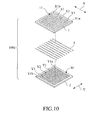
- Figure 2 shows the continuous planar structure of the first conductive layer 10 opposing the second conductive layer 2 when the first and second substrates 1, 2 are assembled together.
- the first and second substrates 1, 2 are spaced from each other by a plurality of insulation spacer 3.
- Each elongate conductive strip Y1, Y2, Y3, ..., Yn of the second conductive layer 2 has a first end Y1a, Y2a, Y3a, ..., Yna, which is connected to a scan sensing circuit 6 by scanning lines 61, an example being a conventional multiplexer.
- Each elongate conductive strip Y1, Y2, Y3, ..., Yn of the second conductive layer 2 also has a second end Y1b, Y2b, Y3b, ..., Ynb, which is set in an open condition.
- the scanning operation is repeated in sequence for each of the elongate conductive strips and finally, at the nth time point t1n, the first end Yna of the elongate conductive strip Yn is scanned. Once the cycle of scanning is completed, the previous process is repeated again for sequentially scanning the ends of the elongate conductive strips Y1, Y2, Y3, ..., Yn.
- the scanning operation that the scan sensing circuit 6 performs over the elongate conductive strips Y1, Y2, Y3, ..., Yn of the second conductive layer 21 provides a scan sensing signal S3, which is converted by an analog-to-digital converter 7 into a digital scan sensing signal, and the digital scan sensing signal is applied to the micro-controller 5.
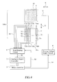
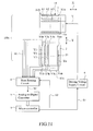
- FIG. 6 shows a system block diagram of a touch control device 100b in accordance with a third embodiment of the present invention.
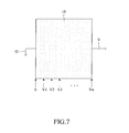
- the third embodiment is substantially identical to the first embodiment (touch control device 100) and the difference between the two embodiments resides in that in the touch control device 100b of the third embodiment, the driving voltage V of a preset voltage level is applied to an end of the continuous planar structure of the first conductive layer 10 and an opposite end of the continuous planar structure of the first conductive layer 10 is grounded via a grounding line G, whereby a potential gradient is established on the continuous planar structure of the first conductive layer 10, as illustrated in Figure 7 .
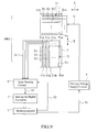
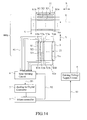
- FIG 12 shows a system block diagram of a touch control device 100f in accordance with a seventh embodiment of the present invention.
- the seventh embodiment is substantially identical to the fifth embodiment (touch control device 100d) illustrated in Figure 9 and the difference between the two embodiments resides in that in the touch control device 100f of the seventh embodiment, the driving voltage V of a preset voltage level is applied to the first end X1a, X2a, X3a, ..., Xna of each elongate conductive strip X1, X2, X3, ..., Xn and the second end X1b, X2b, X3b, ..., Xnb of the elongate conductive strip is grounded via a grounding line G, whereby a potential gradient is established on each elongate conductive strip X1, X2, X3, ..., Xn, as illustrated in Figure 13 .
Landscapes
- Engineering & Computer Science (AREA)
- General Engineering & Computer Science (AREA)
- Theoretical Computer Science (AREA)
- Human Computer Interaction (AREA)
- Physics & Mathematics (AREA)
- General Physics & Mathematics (AREA)
- Position Input By Displaying (AREA)
- Electronic Switches (AREA)
Applications Claiming Priority (1)
| Application Number | Priority Date | Filing Date | Title |
|---|---|---|---|
| TW096143869A TW200923750A (en) | 2007-11-20 | 2007-11-20 | Touch control device and its method |
Publications (2)
| Publication Number | Publication Date |
|---|---|
| EP2063349A2 true EP2063349A2 (de) | 2009-05-27 |
| EP2063349A3 EP2063349A3 (de) | 2012-07-04 |
Family
ID=39730598
Family Applications (1)
| Application Number | Title | Priority Date | Filing Date |
|---|---|---|---|
| EP08013811A Withdrawn EP2063349A3 (de) | 2007-11-20 | 2008-08-01 | Berührungssteuereinrichtung und verfahren dafür |
Country Status (5)
| Country | Link |
|---|---|
| US (1) | US20090127086A1 (de) |
| EP (1) | EP2063349A3 (de) |
| JP (1) | JP5534658B2 (de) |
| KR (1) | KR100993907B1 (de) |
| TW (1) | TW200923750A (de) |
Cited By (3)
| Publication number | Priority date | Publication date | Assignee | Title |
|---|---|---|---|---|
| CN102023780A (zh) * | 2009-09-23 | 2011-04-20 | 禾瑞亚科技股份有限公司 | 位置侦测的装置及方法 |
| EP2287715A3 (de) * | 2009-07-08 | 2012-08-08 | Chimei InnoLux Corporation | Positionierungsverfahren für Berührungsbildschirm |
| US8536882B2 (en) | 2009-04-17 | 2013-09-17 | Egalax—Empia Technology Inc. | Method and device for position detection |
Families Citing this family (8)
| Publication number | Priority date | Publication date | Assignee | Title |
|---|---|---|---|---|
| US20100164899A1 (en) * | 2008-12-25 | 2010-07-01 | Cheng-Ko Wu | Matrix resistive touch device |
| TWI511019B (zh) * | 2009-11-17 | 2015-12-01 | Wistron Corp | 全平面之電阻式觸控面板 |
| TW201128484A (en) * | 2010-02-05 | 2011-08-16 | Sitronix Technology Corp | Touch panel capable of eliminating ghost points |
| TWI501123B (zh) * | 2010-02-09 | 2015-09-21 | Sitronix Technology Corp | A scanning method that is used to increase the scanning speed of the touch panel |
| CN102163113A (zh) * | 2010-02-20 | 2011-08-24 | 宇辰光电股份有限公司 | 全平面的电阻式触控面板 |
| TWI416210B (zh) * | 2010-06-11 | 2013-11-21 | Beijing Funate Innovation Tech | 觸摸式液晶顯示屏 |
| WO2012111194A1 (ja) * | 2011-02-16 | 2012-08-23 | Necカシオモバイルコミュニケーションズ株式会社 | 入力装置、入力方法および記録媒体 |
| CN106855763B (zh) * | 2017-03-10 | 2020-02-07 | 武汉华星光电技术有限公司 | 一种阵列基板及自容式内嵌触控显示面板 |
Family Cites Families (16)
| Publication number | Priority date | Publication date | Assignee | Title |
|---|---|---|---|---|
| US4857716A (en) * | 1986-05-12 | 1989-08-15 | Clinicom Incorporated | Patient identification and verification system and method |
| EP0435438B1 (de) * | 1989-12-28 | 1998-03-04 | Gunze Limited | Eingabesystem mit berührungsempfindlicher Widerstandsfilmtafel |
| JPH03212722A (ja) * | 1990-01-18 | 1991-09-18 | Optrex Corp | アナログタッチスイッチ及びタッチスイッチ付表示装置 |
| JP3190407B2 (ja) * | 1992-02-27 | 2001-07-23 | グンゼ株式会社 | タッチパネル装置 |
| JP2000112642A (ja) * | 1998-09-30 | 2000-04-21 | Digital Electronics Corp | タッチパネル |
| JP3794871B2 (ja) * | 1999-07-12 | 2006-07-12 | 株式会社日立製作所 | タッチパネルおよびこれを用いた液晶表示装置 |
| US20050027570A1 (en) * | 2000-08-11 | 2005-02-03 | Maier Frith Ann | Digital image collection and library system |
| US20030082544A1 (en) * | 2001-07-11 | 2003-05-01 | Third Wave Technologies, Inc. | Methods and systems for validating detection assays, developing in-vitro diagnostic DNA or RNA analysis products, and increasing revenue and/or profit margins from in-vitro diagnostic DNA or RNA analysis assays |
| JP2002366302A (ja) * | 2001-06-05 | 2002-12-20 | Mitsubishi Electric Corp | タッチパネル付き設定表示装置 |
| JP2003216337A (ja) | 2002-01-18 | 2003-07-31 | Tokai Rika Co Ltd | タッチパネル |
| US7558623B2 (en) * | 2002-09-20 | 2009-07-07 | Angel Medical Systems, Inc. | Means and method for the detection of cardiac events |
| US7991460B2 (en) * | 2002-09-20 | 2011-08-02 | Angel Medical Systems, Inc. | Methods and apparatus for detecting cardiac events based on heart rate sensitive parameters |
| US8135595B2 (en) * | 2004-05-14 | 2012-03-13 | H. Lee Moffitt Cancer Center And Research Institute, Inc. | Computer systems and methods for providing health care |
| US7492358B2 (en) * | 2004-06-15 | 2009-02-17 | International Business Machines Corporation | Resistive scanning grid touch panel |
| US7952564B2 (en) * | 2005-02-17 | 2011-05-31 | Hurst G Samuel | Multiple-touch sensor |
| US9943244B2 (en) * | 2007-09-14 | 2018-04-17 | Angel Medical Systems, Inc. | Waveform feature value averaging system and methods for the detection of cardiac events |
-
2007
- 2007-11-20 TW TW096143869A patent/TW200923750A/zh not_active IP Right Cessation
-
2008
- 2008-06-30 US US12/216,090 patent/US20090127086A1/en not_active Abandoned
- 2008-07-18 JP JP2008186957A patent/JP5534658B2/ja not_active Expired - Fee Related
- 2008-08-01 EP EP08013811A patent/EP2063349A3/de not_active Withdrawn
- 2008-08-07 KR KR1020080077391A patent/KR100993907B1/ko not_active Expired - Fee Related
Cited By (11)
| Publication number | Priority date | Publication date | Assignee | Title |
|---|---|---|---|---|
| US8536882B2 (en) | 2009-04-17 | 2013-09-17 | Egalax—Empia Technology Inc. | Method and device for position detection |
| US8536884B2 (en) | 2009-04-17 | 2013-09-17 | Egalax—Empia Technology Inc. | Method and device for correcting position error |
| US8581604B2 (en) | 2009-04-17 | 2013-11-12 | Egalax—Empia Technology Inc. | Method and device for determining impedance of depression |
| US8633718B2 (en) | 2009-04-17 | 2014-01-21 | Egalax—Empia Technology Inc. | Method and device for position detection with palm rejection |
| US8633716B2 (en) | 2009-04-17 | 2014-01-21 | Egalax—Empia Technology Inc. | Method and device for position detection |
| US8633719B2 (en) | 2009-04-17 | 2014-01-21 | Egalax—Empia Technology Inc. | Method and device for position detection |
| US8633717B2 (en) | 2009-04-17 | 2014-01-21 | Egalax—Empia Technology Inc. | Method and device for determining impedance of depression |
| US9080919B2 (en) | 2009-04-17 | 2015-07-14 | Egalax—Empia Technology Inc. | Method and device for position detection with palm rejection |
| EP2287715A3 (de) * | 2009-07-08 | 2012-08-08 | Chimei InnoLux Corporation | Positionierungsverfahren für Berührungsbildschirm |
| CN102023780A (zh) * | 2009-09-23 | 2011-04-20 | 禾瑞亚科技股份有限公司 | 位置侦测的装置及方法 |
| CN102023780B (zh) * | 2009-09-23 | 2013-01-23 | 禾瑞亚科技股份有限公司 | 位置侦测的装置及方法 |
Also Published As
| Publication number | Publication date |
|---|---|
| US20090127086A1 (en) | 2009-05-21 |
| KR100993907B1 (ko) | 2010-11-16 |
| JP5534658B2 (ja) | 2014-07-02 |
| EP2063349A3 (de) | 2012-07-04 |
| JP2009129442A (ja) | 2009-06-11 |
| TW200923750A (en) | 2009-06-01 |
| TWI363990B (de) | 2012-05-11 |
| KR20090052263A (ko) | 2009-05-25 |
Similar Documents
| Publication | Publication Date | Title |
|---|---|---|
| EP2063349A2 (de) | Berührungssteuerungsvorrichtung und Verfahren dafür | |
| KR100952017B1 (ko) | 터치 제어 패널의 터치 포인트를 스캐닝하고 감지하는 장치및 그 방법 | |
| KR100953801B1 (ko) | 터치 제어 장치의 터치 포인트를 감지하는 방법 | |
| EP2169519B1 (de) | Berührungspositionserkennungsverfahren für Berührungssteuerungsvorrichtung | |
| CN102760405B (zh) | 显示装置及其显示图像暨触摸感应的方法 | |
| CN105955522A (zh) | 触控显示装置及其驱动方法 | |
| JP2004206681A (ja) | タッチパネルの駆動方法 | |
| CN101833387A (zh) | 感压式触控装置 | |
| KR20110010559A (ko) | 터치장치 및 그 제조방법 | |
| WO2010023834A1 (ja) | タッチパネルの多点同時検出方法及び多点同時検出タッチパネル装置 | |
| TW201322074A (zh) | 電壓式電容感應觸控裝置及觸控感應方法 | |
| CN109521910A (zh) | 双模式触控显示装置及其实现方法 | |
| CN101464768B (zh) | 触控装置的触控感测方法 | |
| CN101464742A (zh) | 触控装置及其方法 | |
| CN105528115B (zh) | 一种触控显示面板和触控显示设备 | |
| CN209640825U (zh) | 双模式触控显示装置 | |
| JP5284768B2 (ja) | タッチパネル装置のタッチ検知方法 | |
| CN202195795U (zh) | 指示体检测装置及位置检测传感器 | |
| CN101452129B (zh) | 触摸屏和触摸屏显示装置 | |
| CN101470563A (zh) | 触摸板的触控点扫描检测装置及其方法 | |
| CN203588231U (zh) | 一种触摸显示装置 | |
| CN109614002A (zh) | 内嵌型触控显示面板与触控检测方法 | |
| TWI385564B (zh) | 投影電容式觸控面板之判定多觸點位置的裝置及其方法 | |
| CN103970387A (zh) | 触控感测和反馈的装置与方法 |
Legal Events
| Date | Code | Title | Description |
|---|---|---|---|
| PUAI | Public reference made under article 153(3) epc to a published international application that has entered the european phase |
Free format text: ORIGINAL CODE: 0009012 |
|
| 17P | Request for examination filed |
Effective date: 20080808 |
|
| AK | Designated contracting states |
Kind code of ref document: A2 Designated state(s): AT BE BG CH CY CZ DE DK EE ES FI FR GB GR HR HU IE IS IT LI LT LU LV MC MT NL NO PL PT RO SE SI SK TR |
|
| AX | Request for extension of the european patent |
Extension state: AL BA MK RS |
|
| PUAL | Search report despatched |
Free format text: ORIGINAL CODE: 0009013 |
|
| AK | Designated contracting states |
Kind code of ref document: A3 Designated state(s): AT BE BG CH CY CZ DE DK EE ES FI FR GB GR HR HU IE IS IT LI LT LU LV MC MT NL NO PL PT RO SE SI SK TR |
|
| AX | Request for extension of the european patent |
Extension state: AL BA MK RS |
|
| RIC1 | Information provided on ipc code assigned before grant |
Ipc: G06F 3/047 20060101ALI20120525BHEP Ipc: G06F 3/045 20060101AFI20120525BHEP |
|
| AKX | Designation fees paid |
Designated state(s): DE FR GB |
|
| 17Q | First examination report despatched |
Effective date: 20130322 |
|
| STAA | Information on the status of an ep patent application or granted ep patent |
Free format text: STATUS: THE APPLICATION IS DEEMED TO BE WITHDRAWN |
|
| 18D | Application deemed to be withdrawn |
Effective date: 20140611 |