EP2063469A2 - Verfahren zur Herstellung einer Vertikallicht emittierenden Diode - Google Patents
Verfahren zur Herstellung einer Vertikallicht emittierenden Diode Download PDFInfo
- Publication number
- EP2063469A2 EP2063469A2 EP08010010A EP08010010A EP2063469A2 EP 2063469 A2 EP2063469 A2 EP 2063469A2 EP 08010010 A EP08010010 A EP 08010010A EP 08010010 A EP08010010 A EP 08010010A EP 2063469 A2 EP2063469 A2 EP 2063469A2
- Authority
- EP
- European Patent Office
- Prior art keywords
- light emitting
- forming
- nitride semiconductor
- type nitride
- electrode
- Prior art date
- Legal status (The legal status is an assumption and is not a legal conclusion. Google has not performed a legal analysis and makes no representation as to the accuracy of the status listed.)
- Granted
Links
Images



Classifications
-
- H—ELECTRICITY
- H10—SEMICONDUCTOR DEVICES; ELECTRIC SOLID-STATE DEVICES NOT OTHERWISE PROVIDED FOR
- H10H—INORGANIC LIGHT-EMITTING SEMICONDUCTOR DEVICES HAVING POTENTIAL BARRIERS
- H10H20/00—Individual inorganic light-emitting semiconductor devices having potential barriers, e.g. light-emitting diodes [LED]
- H10H20/01—Manufacture or treatment
- H10H20/011—Manufacture or treatment of bodies, e.g. forming semiconductor layers
- H10H20/018—Bonding of wafers
-
- H—ELECTRICITY
- H10—SEMICONDUCTOR DEVICES; ELECTRIC SOLID-STATE DEVICES NOT OTHERWISE PROVIDED FOR
- H10H—INORGANIC LIGHT-EMITTING SEMICONDUCTOR DEVICES HAVING POTENTIAL BARRIERS
- H10H20/00—Individual inorganic light-emitting semiconductor devices having potential barriers, e.g. light-emitting diodes [LED]
- H10H20/01—Manufacture or treatment
- H10H20/011—Manufacture or treatment of bodies, e.g. forming semiconductor layers
- H10H20/013—Manufacture or treatment of bodies, e.g. forming semiconductor layers having light-emitting regions comprising only Group III-V materials
- H10H20/0133—Manufacture or treatment of bodies, e.g. forming semiconductor layers having light-emitting regions comprising only Group III-V materials with a substrate not being Group III-V materials
- H10H20/01335—Manufacture or treatment of bodies, e.g. forming semiconductor layers having light-emitting regions comprising only Group III-V materials with a substrate not being Group III-V materials the light-emitting regions comprising nitride materials
-
- H—ELECTRICITY
- H10—SEMICONDUCTOR DEVICES; ELECTRIC SOLID-STATE DEVICES NOT OTHERWISE PROVIDED FOR
- H10H—INORGANIC LIGHT-EMITTING SEMICONDUCTOR DEVICES HAVING POTENTIAL BARRIERS
- H10H20/00—Individual inorganic light-emitting semiconductor devices having potential barriers, e.g. light-emitting diodes [LED]
- H10H20/80—Constructional details
- H10H20/84—Coatings, e.g. passivation layers or antireflective coatings
Definitions
- the present invention relates to a method of manufacturing a vertical light emitting diode (LED), which can prevent the damage of a light emitting structure during an LLO (laser lift-off) process for removing a sapphire substrate.
- LED vertical light emitting diode
- a nitride-based semiconductor LED is grown on a sapphire substrate, but the sapphire substrate is a rigid nonconductor and has poor thermal conductivity. Therefore, there is a limitation in reducing the manufacturing costs by reducing the size of a nitride-based semiconductor LED, or improving the optical power and chip characteristic. Particularly, because the application of a high current is essential for achieving high power LED, it is important to solve a heat-sink problem of the LED. To solve this problem, there has been proposed a vertical LED in which a sapphire substrate is removed using an LLO technique.
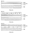
- FIGS. 1A to 1F a conventional method of manufacturing a vertical LED will be described with reference to FIGS. 1A to 1F .
- FIGS. 1A to 1F are process diagrams sequentially showing a conventional method of manufacturing a vertical LED.
- a light emitting structure 110 is formed on a transparent substrate 110 such as sapphire.
- the light emitting structure 110 includes an n-type nitride semiconductor layer 112, a GaN/InGaN active layer 114 with a multi-quantum well structure, and a p-type nitride semiconductor layer 115, which are sequentially laminated.
- photoresist patterns PR for defining a desired size of unit LED elements are formed on the p-type nitride semiconductor layer 115.
- the light emitting structure 110 is isolated into unit LED elements through an ISO (isolation) process using dry etching such as ICP (inductive coupled plasma) or layer, with the photoresist patterns being set to an etching mask. Then, the photoresist patterns are removed.
- ISO isolation
- ICP inductive coupled plasma
- an insulating film or reflecting film may be formed on the side surfaces of the isolated light emitting structures 110.
- the insulating film or reflecting film can be omitted depending on the characteristics of LED and process conditions.
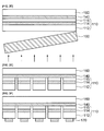
- a p-electrode 140 is formed on each of the isolated light emitting structures 110. Then, as shown in FIG. 1E , a structure support layer 160 is formed on the p-electrode 140.
- the substrate 110 is removed through the LLO process.
- the LLO process when an energy of about 700mJ/cm 2 is applied at the normal temperature in an arrow direction, the energy is absorbed at the interface between the substrate 100 and the light emitting structure 110 such that the bonded surface of the light emitting structure 110 is thermally discomposed, and the substrate 100 and the light emitting structure 110 are then separated from each other.
- an n-electrode is formed on each of the n-type nitride semiconductor layers 112 which are exposed by the removing of the substrate, thereby forming vertical LEDs.
- FIG. 2 is a photograph showing the problem of the vertical LED manufactured according to the conventional method.
- a crack may also occur in the insulating film or reflecting film formed on the side surfaces of the isolated light emitting structures or the adhesion therebetween may be degraded during the LLO process.
- An advantage of the present invention is that it provides a method of manufacturing a vertical LED, which can prevent the damage of a light emitting structure during an LLO process for removing a sapphire substrate.
- a method of manufacturing a vertical LED comprises the steps of: preparing a sapphire substrate; forming a light emitting structure in which an n-type nitride semiconductor layer, an active layer, and a p-type nitride semiconductor layer are sequentially laminated on the sapphire substrate; forming a p-electrode on the p-type nitride semiconductor layer; forming a structure support layer on the p-electrode; removing the sapphire substrate through an LLO (laser lift-off) process; isolating the light emitting structure into unit LED elements through an ISO (isolation) process; and forming an n-electrode on each of the n-type nitride semiconductor layers of the isolated light emitting structures.
- LLO laser lift-off
- the method further comprises the step of forming an insulating film or reflecting film on the side surfaces of the isolated light emitting structures, after the isolating of the light emitting structure.
- a method of manufacturing a vertical LED comprises the steps of: preparing a sapphire substrate; forming a light emitting structure in which an n-type nitride semiconductor layer, an active layer, and a p-type nitride semiconductor layer are sequentially laminated on the sapphire substrate; forming buffer films on portions of the surface of the p-type nitride semiconductor layer corresponding to element isolation regions; forming a p-electrode on the resulting structure having the buffer films formed thereon; forming a structure support layer on the resulting structure having the p-electrode formed thereon; removing the sapphire substrate through an LLO process; isolating the light emitting structure into unit LED elements through an ISO process; and forming an n-electrode on each of the n-type nitride semiconductor layers of the isolated light emitting structures.
- the p-electrode is formed on the surface of the p-type nitride semiconductor layer excluding the portions on which the buffer films are formed.
- the buffer films are composed of a non-conductive material.
- the non-conducive material photoresist, polyimide, epoxy, and dielectric may be used.
- a method of manufacturing a vertical LED comprises the steps of: preparing a sapphire substrate; forming a light emitting structure in which an n-type nitride semiconductor layer, an active layer, and a p-type nitride semiconductor layer are sequentially laminated on the sapphire substrate; performing a first ISO process for isolating the light emitting structure into unit LED elements such that portions of the light emitting structure corresponding to element isolation regions remain with a predetermined thickness on the sapphire substrate; forming a p-electrode on the surface of the p-type nitride semiconductor layer corresponding to each unit LED element region; forming a structure support layer on the p-electrode; removing the sapphire substrate through an LLO process; performing a second ISO process for completely isolating the light emitting structure into unit LED elements by removing the remaining portions of the light emitting structure corresponding to the element isolation regions; and forming an n-electrode on each
- the method further comprises the step of forming a first insulating film or first reflecting film on the side surfaces of the isolated light emitting structures after the performing of the first ISO process.
- the method further comprises the step of forming a second insulating film or second reflecting film on the side surfaces of the isolated light emitting structures after the performing of the second ISO process.
- FIGS. 1A to 1F are process diagrams sequentially showing a conventional method of manufacturing a vertical LED
- FIG. 2 is a photograph showing the problem of a vertical LED manufactured according to the conventional method
- FIGS. 3A to 3F are process diagrams sequentially showing a method of manufacturing a vertical LED according to a first embodiment of the invention
- FIG. 4 is a process diagram for explaining a modification of the method of manufacturing a vertical LED according to the first embodiment of the invention
- FIG. 5 is a process diagram for explaining a method of manufacturing a vertical LED according to a second embodiment of the invention.
- FIGS. 6A to 6E are process diagrams sequentially showing a method of manufacturing a vertical LED according to a third embodiment of the invention.
- FIGS. 3A to 3F a method of manufacturing a vertical LED according to a first embodiment of the invention will be described.
- FIGS. 3A to 3F are process diagrams sequentially showing a method of manufacturing a vertical LED according to a first embodiment of the invention.
- a light emitting structure 110 composed of a nitride-based semiconductor layer is formed on a transparent substrate 100 such as sapphire.
- the light emitting structure 110 includes an n-type nitride semiconductor layer 112, a GaN/InGaN active layer 114 with a multi-quantum well structure, and a p-type nitride semiconductor layer 115, which are sequentially laminated.
- the n-type and p-type nitride semiconductor layer 112 and 115 and the active layer 114 may be formed of a nitride semiconductor material having a compositional formula of Al x In y Ga (1-x-y) N (here, 0 ⁇ x ⁇ 1,0 ⁇ y ⁇ 1, and 0 ⁇ x+y ⁇ 1) and can be formed through a well-known nitride deposition process such as MOCVD (Metal Organic Chemical Vapor Deposition).
- MOCVD Metal Organic Chemical Vapor Deposition
- the active layer 114 may be formed of one quantum-well layer or with a double-hetero structure.
- a p-electrode 140 is formed on the p-type nitride semiconductor 115 of the light emitting structure 110.
- the p-electrode 140 is formed so as to serve as an electrode and a reflecting film.
- a bonding layer (not shown) for bonding a structure support layer through an eutectic bonding method is formed on the p-electrode 140, and high temperature and pressure is applied to the bonding layer so as to perform a bonding process for bonding the structure support layer 160 on the p-electrode 140. Since the structure support layer 160 is to serve as a support layer and electrode of a finalized LED, the structure support layer 160 is formed of a silicon substrate having excellent heat conductivity and conductance.
- the bonding layer may be formed of gold (Au) or an alloy containing Au (for example, AuSn).
- the substrate 100 is removed through an LLO process.
- the LLO process when an energy of about 700mJ/cm 2 is applied at the normal temperature in an arrow direction, the energy is absorbed at the interface between the substrate 100 and the light emitting structure 110 such that the bonded surface of the light emitting structure 110 is thermally discomposed, and the substrate 100 and the light emitting structure 110 are then separated from each other.
- a photoresist pattern (not shown) for defining a desired size of unit LED elements is formed on the n-type nitride semiconductor 112.
- the light emitting structure 110 is isolated into unit LED elements by a drying etching process using ICP (Inductive Coupled Plasma) or an isolation (ISO) process using laser, with the photoresist pattern being set to an etching mask, and the photoresist pattern is then removed.
- ICP Inductive Coupled Plasma
- ISO isolation
- an n-electrode 170 is formed on each of the n-type nitride semiconductor layers 112 of the isolated light emitting structures 110, thereby forming the vertical LED.
- the ISO process for isolating the light emitting structure into unit LED elements is performed after the LLO process for separating the sapphire substrate. Therefore, it is possible to prevent the damage of the light emitting structure such as cracks which have occurred due to an impact of laser during the LLO process in the related art.
- FIG. 4 is a process diagram for explaining the modification of the method of manufacturing a vertical LED according to the first embodiment of the invention.
- FIG. 5 a method of manufacturing a vertical LED according to a second embodiment of the invention will be described. The descriptions of the same construction as that of the first embodiment will be omitted.
- FIG. 5 is a process diagram for explaining a method of manufacturing a vertical LED according to a second embodiment of the invention.
- the method of manufacturing a vertical LED according to the second embodiment is performed in almost the same manner as the first embodiment. As shown in FIG. 5 , however, the method of manufacturing a vertical LED according to the second embodiment further includes the step of forming buffer films 300 on portions of the surface of the p-type nitride semiconductor layer 115 corresponding to element isolation regions, before the p-electrode 140 is formed on the p-type nitride semiconductor layer 115.
- the ISO process for isolating the light emitting structure into unit LED elements is performed after the LLO process for separating the substrate, like the first embodiment. Therefore, it is possible to obtain the same effect as that of the first embodiment.
- the buffer film 300 is formed of a non-conductive material. More specifically, the buffer film 300 may be formed of photoresist, polyimide, epoxy, or dielectric.
- the method according to the second embodiment further includes the process of forming the buffer films 300, the p-electrode can be more reliably protected from an impact of laser during the ISO process than in the first embodiment.
- FIGS. 6A to 6E a method of manufacturing a vertical LED according to a third embodiment of the invention will be described. The descriptions of the same construction as that of the first embodiment will be omitted.
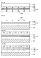
- FIGS. 6A to 6E are process diagrams sequentially showing a method of manufacturing a vertical LED according to a third embodiment of the invention.
- the method of manufacturing a vertical LED according to the third embodiment is performed in almost the same manner as the first embodiment.
- the method according to the third embodiment is different from the first embodiment in that the process of isolating the light emitting structure 110 into unit LED elements is divided into two steps, and the LLO process for removing the substrate 110 from the light emitting structure 110 is performed between two steps.
- the method of manufacturing a vertical LED according to the third embodiment of the invention is performed as follows.
- the light emitting structure 110 is formed on the substrate 100, as shown in FIG. 3A of the first embodiment.
- photoresist patterns PR for defining a desired size of unit LED elements are formed on the p-type nitride semiconductor layer 115 of the light emitting structure 110.
- a first ISO process for isolating the light emitting structure 110 into unit LED elements is performed using laser or a drying etching process using ICP, with the photoresist patterns being set to an etching mask, such that portions of the light emitting structure 110 corresponding to element isolation regions remain with a predetermined thickness.
- the p-electrode 140 is formed on the surface of the p-type nitride semiconductor layer 115 of each unit LED element, and the structure support layer 160 is formed on the p-electrode 140.
- the substrate 100 is removed through the LLO process.
- the remaining portions of the light emitting structure 110 corresponding to element isolation regions are removed through a second ISO process such that the light emitting structure 110 is isolated into unit LED elements.
- an n-electrode 170 is formed on each of the n-type nitride semiconductor layers 112 of the isolated light emitting structures 110.
- the second ISO process in which the light emitting structure is completely isolated into the unit LED elements is performed after the LLO process for removing the substrate, as in the first embodiment. Therefore, it is possible to obtain the same effect as the first embodiment.
- the method according to the third embodiment of the invention may further include the steps of: forming a first insulating film or a first reflecting film on the side surfaces of the isolated light emitting structures after the first ISO process and forming a second insulating film or a second reflecting film on the side surfaces of the isolated light emitting structures after the second ISO process, depending on characteristics of LED and a process condition.
- the LLO process for separating the sapphire substrate from the light emitting substrate is performed before the ISO process for isolating the light emitting structure into unit LED elements. Therefore, it is possible to prevent the damage of the light emitting structure such as cracks caused by an impact of laser during the LLO process.
- the method according to the invention can enhance not only the characteristic and reliability of the vertical LED but also the production yield of the vertical LED.
Landscapes
- Led Devices (AREA)
Applications Claiming Priority (1)
| Application Number | Priority Date | Filing Date | Title |
|---|---|---|---|
| KR1020070120260A KR100888440B1 (ko) | 2007-11-23 | 2007-11-23 | 수직구조 발광다이오드 소자의 제조방법 |
Publications (3)
| Publication Number | Publication Date |
|---|---|
| EP2063469A2 true EP2063469A2 (de) | 2009-05-27 |
| EP2063469A3 EP2063469A3 (de) | 2013-03-27 |
| EP2063469B1 EP2063469B1 (de) | 2019-03-06 |
Family
ID=39683627
Family Applications (1)
| Application Number | Title | Priority Date | Filing Date |
|---|---|---|---|
| EP08010010.0A Active EP2063469B1 (de) | 2007-11-23 | 2008-06-02 | Verfahren zur Herstellung einer Vertikallicht emittierenden Diode |
Country Status (5)
| Country | Link |
|---|---|
| US (1) | US7838315B2 (de) |
| EP (1) | EP2063469B1 (de) |
| KR (1) | KR100888440B1 (de) |
| DE (1) | DE202008017889U1 (de) |
| TW (1) | TWI401819B (de) |
Cited By (1)
| Publication number | Priority date | Publication date | Assignee | Title |
|---|---|---|---|---|
| EP2302672A3 (de) * | 2009-09-25 | 2011-06-29 | Kabushiki Kaisha Toshiba | Halbleiterbauelement mit Anschlussfläche und Verfahren zu seiner Herstellung |
Families Citing this family (35)
| Publication number | Priority date | Publication date | Assignee | Title |
|---|---|---|---|---|
| US20070240631A1 (en) * | 2006-04-14 | 2007-10-18 | Applied Materials, Inc. | Epitaxial growth of compound nitride semiconductor structures |
| US20080092819A1 (en) * | 2006-10-24 | 2008-04-24 | Applied Materials, Inc. | Substrate support structure with rapid temperature change |
| US20080314311A1 (en) * | 2007-06-24 | 2008-12-25 | Burrows Brian H | Hvpe showerhead design |
| US20090149008A1 (en) * | 2007-10-05 | 2009-06-11 | Applied Materials, Inc. | Method for depositing group iii/v compounds |
| US20090194026A1 (en) * | 2008-01-31 | 2009-08-06 | Burrows Brian H | Processing system for fabricating compound nitride semiconductor devices |
| US20100139554A1 (en) * | 2008-12-08 | 2010-06-10 | Applied Materials, Inc. | Methods and apparatus for making gallium nitride and gallium aluminum nitride thin films |
| US20100273291A1 (en) * | 2009-04-28 | 2010-10-28 | Applied Materials, Inc. | Decontamination of mocvd chamber using nh3 purge after in-situ cleaning |
| US20110079251A1 (en) * | 2009-04-28 | 2011-04-07 | Olga Kryliouk | Method for in-situ cleaning of deposition systems |
| JP2012525718A (ja) * | 2009-04-29 | 2012-10-22 | アプライド マテリアルズ インコーポレイテッド | HVPEにおいてその場プレ−GaN堆積層を形成する方法 |
| US8587017B2 (en) | 2009-07-05 | 2013-11-19 | Industrial Technology Research Institute | Light emitting device and method of fabricating a light emitting device |
| US20110104843A1 (en) * | 2009-07-31 | 2011-05-05 | Applied Materials, Inc. | Method of reducing degradation of multi quantum well (mqw) light emitting diodes |
| US20110027973A1 (en) * | 2009-07-31 | 2011-02-03 | Applied Materials, Inc. | Method of forming led structures |
| CN102414801A (zh) | 2009-08-27 | 2012-04-11 | 应用材料公司 | 在原位腔室清洁后的处理腔室去污方法 |
| US20110064545A1 (en) * | 2009-09-16 | 2011-03-17 | Applied Materials, Inc. | Substrate transfer mechanism with preheating features |
| US20110076400A1 (en) * | 2009-09-30 | 2011-03-31 | Applied Materials, Inc. | Nanocrystalline diamond-structured carbon coating of silicon carbide |
| US20110081771A1 (en) * | 2009-10-07 | 2011-04-07 | Applied Materials, Inc. | Multichamber split processes for led manufacturing |
| WO2011069242A1 (en) * | 2009-12-09 | 2011-06-16 | Cooledge Lighting Inc. | Semiconductor dice transfer-enabling apparatus and method for manufacturing transfer-enabling apparatus |
| US20110151588A1 (en) * | 2009-12-17 | 2011-06-23 | Cooledge Lighting, Inc. | Method and magnetic transfer stamp for transferring semiconductor dice using magnetic transfer printing techniques |
| US8334152B2 (en) | 2009-12-18 | 2012-12-18 | Cooledge Lighting, Inc. | Method of manufacturing transferable elements incorporating radiation enabled lift off for allowing transfer from host substrate |
| US20110204376A1 (en) * | 2010-02-23 | 2011-08-25 | Applied Materials, Inc. | Growth of multi-junction led film stacks with multi-chambered epitaxy system |
| US20110207256A1 (en) * | 2010-02-24 | 2011-08-25 | Applied Materials, Inc. | In-situ acceptor activation with nitrogen and/or oxygen plasma treatment |
| US9076827B2 (en) | 2010-09-14 | 2015-07-07 | Applied Materials, Inc. | Transfer chamber metrology for improved device yield |
| US9070851B2 (en) | 2010-09-24 | 2015-06-30 | Seoul Semiconductor Co., Ltd. | Wafer-level light emitting diode package and method of fabricating the same |
| KR101249924B1 (ko) * | 2010-11-03 | 2013-04-03 | (주)버티클 | 반도체 소자 및 그 제조 방법 |
| KR101244926B1 (ko) * | 2011-04-28 | 2013-03-18 | 피에스아이 주식회사 | 초소형 led 소자 및 그 제조방법 |
| US8778783B2 (en) | 2011-05-20 | 2014-07-15 | Applied Materials, Inc. | Methods for improved growth of group III nitride buffer layers |
| US8853086B2 (en) | 2011-05-20 | 2014-10-07 | Applied Materials, Inc. | Methods for pretreatment of group III-nitride depositions |
| US8980002B2 (en) | 2011-05-20 | 2015-03-17 | Applied Materials, Inc. | Methods for improved growth of group III nitride semiconductor compounds |
| KR101672781B1 (ko) * | 2014-11-18 | 2016-11-07 | 피에스아이 주식회사 | 수평배열 어셈블리용 초소형 led 소자, 이의 제조방법 및 이를 포함하는 수평배열 어셈블리 |
| KR101713818B1 (ko) | 2014-11-18 | 2017-03-10 | 피에스아이 주식회사 | 초소형 led 소자를 포함하는 전극어셈블리 및 그 제조방법 |
| KR101730977B1 (ko) | 2016-01-14 | 2017-04-28 | 피에스아이 주식회사 | 초소형 led 전극어셈블리 |
| CN205944139U (zh) | 2016-03-30 | 2017-02-08 | 首尔伟傲世有限公司 | 紫外线发光二极管封装件以及包含此的发光二极管模块 |
| KR102568353B1 (ko) * | 2018-08-16 | 2023-08-18 | 삼성디스플레이 주식회사 | 발광 소자, 이의 제조방법 및 발광 소자를 포함하는 표시 장치 |
| CN111863871A (zh) * | 2019-04-29 | 2020-10-30 | 云谷(固安)科技有限公司 | 一种显示面板及其制备方法 |
| KR102717366B1 (ko) * | 2019-11-04 | 2024-10-16 | 쑤저우 레킨 세미컨덕터 컴퍼니 리미티드 | 표면발광 레이저소자, 이를 포함하는 발광장치 및 그 제조방법 |
Citations (3)
| Publication number | Priority date | Publication date | Assignee | Title |
|---|---|---|---|---|
| US6818531B1 (en) | 2003-06-03 | 2004-11-16 | Samsung Electro-Mechanics Co., Ltd. | Method for manufacturing vertical GaN light emitting diodes |
| WO2006043796A1 (en) | 2004-10-22 | 2006-04-27 | Seoul Opto-Device Co., Ltd. | Gan compound semiconductor light emitting element and method of manufacturing the same |
| EP1753018A2 (de) | 2005-08-12 | 2007-02-14 | Samsung Electro-Mechanics Co., Ltd. | Verfahren zur Herstellung eines auf Nitrid Basis einkristallinen Substrats und Verfahren zur Herstellung einer Halbleiteranordnung auf Nitrid Basis |
Family Cites Families (7)
| Publication number | Priority date | Publication date | Assignee | Title |
|---|---|---|---|---|
| KR100495215B1 (ko) * | 2002-12-27 | 2005-06-14 | 삼성전기주식회사 | 수직구조 갈륨나이트라이드 발광다이오드 및 그 제조방법 |
| US7244628B2 (en) * | 2003-05-22 | 2007-07-17 | Matsushita Electric Industrial Co., Ltd. | Method for fabricating semiconductor devices |
| KR100624448B1 (ko) * | 2004-12-02 | 2006-09-18 | 삼성전기주식회사 | 반도체 발광소자 및 그 제조방법 |
| TWI247441B (en) * | 2005-01-21 | 2006-01-11 | United Epitaxy Co Ltd | Light emitting diode and fabricating method thereof |
| KR100706952B1 (ko) * | 2005-07-22 | 2007-04-12 | 삼성전기주식회사 | 수직 구조 질화갈륨계 발광다이오드 소자 및 그 제조방법 |
| KR100706951B1 (ko) * | 2005-08-17 | 2007-04-12 | 삼성전기주식회사 | 수직구조 질화갈륨계 led 소자의 제조방법 |
| KR100836129B1 (ko) | 2006-06-19 | 2008-06-09 | 삼성전기주식회사 | 모바일 기기용 엑츄에이터 |
-
2007
- 2007-11-23 KR KR1020070120260A patent/KR100888440B1/ko active Active
-
2008
- 2008-05-29 TW TW097119839A patent/TWI401819B/zh active
- 2008-06-02 EP EP08010010.0A patent/EP2063469B1/de active Active
- 2008-06-02 DE DE202008017889U patent/DE202008017889U1/de not_active Expired - Lifetime
- 2008-06-02 US US12/155,277 patent/US7838315B2/en active Active
Patent Citations (3)
| Publication number | Priority date | Publication date | Assignee | Title |
|---|---|---|---|---|
| US6818531B1 (en) | 2003-06-03 | 2004-11-16 | Samsung Electro-Mechanics Co., Ltd. | Method for manufacturing vertical GaN light emitting diodes |
| WO2006043796A1 (en) | 2004-10-22 | 2006-04-27 | Seoul Opto-Device Co., Ltd. | Gan compound semiconductor light emitting element and method of manufacturing the same |
| EP1753018A2 (de) | 2005-08-12 | 2007-02-14 | Samsung Electro-Mechanics Co., Ltd. | Verfahren zur Herstellung eines auf Nitrid Basis einkristallinen Substrats und Verfahren zur Herstellung einer Halbleiteranordnung auf Nitrid Basis |
Cited By (2)
| Publication number | Priority date | Publication date | Assignee | Title |
|---|---|---|---|---|
| EP2302672A3 (de) * | 2009-09-25 | 2011-06-29 | Kabushiki Kaisha Toshiba | Halbleiterbauelement mit Anschlussfläche und Verfahren zu seiner Herstellung |
| US8319246B2 (en) | 2009-09-25 | 2012-11-27 | Kabushiki Kaisha Toshiba | Semiconductor device and method for manufacturing same |
Also Published As
| Publication number | Publication date |
|---|---|
| US7838315B2 (en) | 2010-11-23 |
| KR100888440B1 (ko) | 2009-03-11 |
| US20090137075A1 (en) | 2009-05-28 |
| EP2063469B1 (de) | 2019-03-06 |
| TWI401819B (zh) | 2013-07-11 |
| EP2063469A3 (de) | 2013-03-27 |
| TW200924236A (en) | 2009-06-01 |
| DE202008017889U1 (de) | 2010-09-23 |
Similar Documents
| Publication | Publication Date | Title |
|---|---|---|
| US7838315B2 (en) | Method of manufacturing vertical light emitting diode | |
| JP7134198B2 (ja) | 発光デバイスを支持基板に取り付ける方法 | |
| US9735327B2 (en) | Light emitting device and manufacturing method for same | |
| CN102194986B (zh) | 半导体发光器件以及制造半导体发光器件的方法 | |
| KR101911580B1 (ko) | 반도체 장치를 지지 기판에 접착시키는 방법 | |
| CN101305478A (zh) | 氮化物半导体发光元件以及氮化物半导体发光元件制造方法 | |
| TWI500183B (zh) | 發光二極體的製造方法 | |
| JP5232975B2 (ja) | 発光ダイオードの製造方法及び発光ダイオード、並びにランプ | |
| CN102347415A (zh) | 半导体发光器件及其制造方法 | |
| US7442565B2 (en) | Method for manufacturing vertical structure light emitting diode | |
| US20120211795A1 (en) | Semiconductor light emitting device including substrate having protection layers and method for manufacturing the same | |
| JP5167831B2 (ja) | Iii族窒化物半導体素子、およびその製造方法 | |
| KR100682255B1 (ko) | 수직형 발광 다이오드의 제조방법 | |
| CN1964090B (zh) | 氮化物基半导体器件及其制造方法 | |
| US8324643B2 (en) | Semiconductor light emitting device having an isolation layer formed of a conductive transmissive material | |
| US7564069B2 (en) | Light-emitting diode including pit therein | |
| KR100990635B1 (ko) | 수직구조 발광다이오드 소자의 제조방법 | |
| JP2007200932A (ja) | 窒化物半導体素子の製造方法 | |
| KR101119009B1 (ko) | 이온주입에 의한 분리를 이용한 발광소자 제조 방법 | |
| KR101210426B1 (ko) | 반도체 발광소자용 서브마운트 기판 및 이를 이용한 반도체 발광소자의 제조방법 | |
| US20130092955A1 (en) | Light emitting diode and fabricating method thereof | |
| US7696068B2 (en) | Method for manufacturing vertical light-emitting diode | |
| KR101219078B1 (ko) | 반도체 발광소자용 서브마운트 기판 및 이를 이용한 반도체 발광소자의 제조방법 | |
| TW202245310A (zh) | 巨量轉移晶片的裝置 |
Legal Events
| Date | Code | Title | Description |
|---|---|---|---|
| PUAI | Public reference made under article 153(3) epc to a published international application that has entered the european phase |
Free format text: ORIGINAL CODE: 0009012 |
|
| AK | Designated contracting states |
Kind code of ref document: A2 Designated state(s): AT BE BG CH CY CZ DE DK EE ES FI FR GB GR HR HU IE IS IT LI LT LU LV MC MT NL NO PL PT RO SE SI SK TR |
|
| AX | Request for extension of the european patent |
Extension state: AL BA MK RS |
|
| RIN1 | Information on inventor provided before grant (corrected) |
Inventor name: LEE, SANG BUM Inventor name: KIM, TAE HYUNG Inventor name: LEE, SI HYUK Inventor name: YANG, JONG IN |
|
| RAP1 | Party data changed (applicant data changed or rights of an application transferred) |
Owner name: SAMSUNG LED CO., LTD. |
|
| RAP1 | Party data changed (applicant data changed or rights of an application transferred) |
Owner name: SAMSUNG ELECTRONICS CO., LTD. |
|
| PUAL | Search report despatched |
Free format text: ORIGINAL CODE: 0009013 |
|
| AK | Designated contracting states |
Kind code of ref document: A3 Designated state(s): AT BE BG CH CY CZ DE DK EE ES FI FR GB GR HR HU IE IS IT LI LT LU LV MC MT NL NO PL PT RO SE SI SK TR |
|
| AX | Request for extension of the european patent |
Extension state: AL BA MK RS |
|
| RIC1 | Information provided on ipc code assigned before grant |
Ipc: H01L 27/15 20060101AFI20130219BHEP Ipc: H01L 33/00 20100101ALI20130219BHEP |
|
| 17P | Request for examination filed |
Effective date: 20130927 |
|
| RBV | Designated contracting states (corrected) |
Designated state(s): AT BE BG CH CY CZ DE DK EE ES FI FR GB GR HR HU IE IS IT LI LT LU LV MC MT NL NO PL PT RO SE SI SK TR |
|
| AKX | Designation fees paid |
Designated state(s): AT BE BG CH CY CZ DE DK EE ES FI FR GB GR HR HU IE IS IT LI LT LU LV MC MT NL NO PL PT RO SE SI SK TR |
|
| STAA | Information on the status of an ep patent application or granted ep patent |
Free format text: STATUS: EXAMINATION IS IN PROGRESS |
|
| 17Q | First examination report despatched |
Effective date: 20180123 |
|
| GRAP | Despatch of communication of intention to grant a patent |
Free format text: ORIGINAL CODE: EPIDOSNIGR1 |
|
| STAA | Information on the status of an ep patent application or granted ep patent |
Free format text: STATUS: GRANT OF PATENT IS INTENDED |
|
| RIC1 | Information provided on ipc code assigned before grant |
Ipc: H01L 33/00 20060101AFI20181012BHEP Ipc: H01L 33/44 20090527ALN20181012BHEP |
|
| INTG | Intention to grant announced |
Effective date: 20181029 |
|
| RIC1 | Information provided on ipc code assigned before grant |
Ipc: H01L 33/44 20100101ALN20181012BHEP Ipc: H01L 33/00 20100101AFI20181012BHEP |
|
| GRAS | Grant fee paid |
Free format text: ORIGINAL CODE: EPIDOSNIGR3 |
|
| GRAA | (expected) grant |
Free format text: ORIGINAL CODE: 0009210 |
|
| STAA | Information on the status of an ep patent application or granted ep patent |
Free format text: STATUS: THE PATENT HAS BEEN GRANTED |
|
| RIC1 | Information provided on ipc code assigned before grant |
Ipc: H01L 33/44 20100101ALN20181012BHEP Ipc: H01L 33/00 20100101AFI20181012BHEP |
|
| AK | Designated contracting states |
Kind code of ref document: B1 Designated state(s): AT BE BG CH CY CZ DE DK EE ES FI FR GB GR HR HU IE IS IT LI LT LU LV MC MT NL NO PL PT RO SE SI SK TR |
|
| REG | Reference to a national code |
Ref country code: GB Ref legal event code: FG4D |
|
| REG | Reference to a national code |
Ref country code: CH Ref legal event code: EP Ref country code: AT Ref legal event code: REF Ref document number: 1105722 Country of ref document: AT Kind code of ref document: T Effective date: 20190315 |
|
| REG | Reference to a national code |
Ref country code: DE Ref legal event code: R096 Ref document number: 602008059203 Country of ref document: DE |
|
| REG | Reference to a national code |
Ref country code: IE Ref legal event code: FG4D |
|
| REG | Reference to a national code |
Ref country code: NL Ref legal event code: MP Effective date: 20190306 |
|
| REG | Reference to a national code |
Ref country code: LT Ref legal event code: MG4D |
|
| PG25 | Lapsed in a contracting state [announced via postgrant information from national office to epo] |
Ref country code: SE Free format text: LAPSE BECAUSE OF FAILURE TO SUBMIT A TRANSLATION OF THE DESCRIPTION OR TO PAY THE FEE WITHIN THE PRESCRIBED TIME-LIMIT Effective date: 20190306 Ref country code: LT Free format text: LAPSE BECAUSE OF FAILURE TO SUBMIT A TRANSLATION OF THE DESCRIPTION OR TO PAY THE FEE WITHIN THE PRESCRIBED TIME-LIMIT Effective date: 20190306 Ref country code: NO Free format text: LAPSE BECAUSE OF FAILURE TO SUBMIT A TRANSLATION OF THE DESCRIPTION OR TO PAY THE FEE WITHIN THE PRESCRIBED TIME-LIMIT Effective date: 20190606 Ref country code: FI Free format text: LAPSE BECAUSE OF FAILURE TO SUBMIT A TRANSLATION OF THE DESCRIPTION OR TO PAY THE FEE WITHIN THE PRESCRIBED TIME-LIMIT Effective date: 20190306 |
|
| PG25 | Lapsed in a contracting state [announced via postgrant information from national office to epo] |
Ref country code: NL Free format text: LAPSE BECAUSE OF FAILURE TO SUBMIT A TRANSLATION OF THE DESCRIPTION OR TO PAY THE FEE WITHIN THE PRESCRIBED TIME-LIMIT Effective date: 20190306 Ref country code: BG Free format text: LAPSE BECAUSE OF FAILURE TO SUBMIT A TRANSLATION OF THE DESCRIPTION OR TO PAY THE FEE WITHIN THE PRESCRIBED TIME-LIMIT Effective date: 20190606 Ref country code: LV Free format text: LAPSE BECAUSE OF FAILURE TO SUBMIT A TRANSLATION OF THE DESCRIPTION OR TO PAY THE FEE WITHIN THE PRESCRIBED TIME-LIMIT Effective date: 20190306 Ref country code: GR Free format text: LAPSE BECAUSE OF FAILURE TO SUBMIT A TRANSLATION OF THE DESCRIPTION OR TO PAY THE FEE WITHIN THE PRESCRIBED TIME-LIMIT Effective date: 20190607 Ref country code: HR Free format text: LAPSE BECAUSE OF FAILURE TO SUBMIT A TRANSLATION OF THE DESCRIPTION OR TO PAY THE FEE WITHIN THE PRESCRIBED TIME-LIMIT Effective date: 20190306 |
|
| REG | Reference to a national code |
Ref country code: AT Ref legal event code: MK05 Ref document number: 1105722 Country of ref document: AT Kind code of ref document: T Effective date: 20190306 |
|
| PG25 | Lapsed in a contracting state [announced via postgrant information from national office to epo] |
Ref country code: SK Free format text: LAPSE BECAUSE OF FAILURE TO SUBMIT A TRANSLATION OF THE DESCRIPTION OR TO PAY THE FEE WITHIN THE PRESCRIBED TIME-LIMIT Effective date: 20190306 Ref country code: IT Free format text: LAPSE BECAUSE OF FAILURE TO SUBMIT A TRANSLATION OF THE DESCRIPTION OR TO PAY THE FEE WITHIN THE PRESCRIBED TIME-LIMIT Effective date: 20190306 Ref country code: EE Free format text: LAPSE BECAUSE OF FAILURE TO SUBMIT A TRANSLATION OF THE DESCRIPTION OR TO PAY THE FEE WITHIN THE PRESCRIBED TIME-LIMIT Effective date: 20190306 Ref country code: ES Free format text: LAPSE BECAUSE OF FAILURE TO SUBMIT A TRANSLATION OF THE DESCRIPTION OR TO PAY THE FEE WITHIN THE PRESCRIBED TIME-LIMIT Effective date: 20190306 Ref country code: PT Free format text: LAPSE BECAUSE OF FAILURE TO SUBMIT A TRANSLATION OF THE DESCRIPTION OR TO PAY THE FEE WITHIN THE PRESCRIBED TIME-LIMIT Effective date: 20190706 Ref country code: RO Free format text: LAPSE BECAUSE OF FAILURE TO SUBMIT A TRANSLATION OF THE DESCRIPTION OR TO PAY THE FEE WITHIN THE PRESCRIBED TIME-LIMIT Effective date: 20190306 Ref country code: CZ Free format text: LAPSE BECAUSE OF FAILURE TO SUBMIT A TRANSLATION OF THE DESCRIPTION OR TO PAY THE FEE WITHIN THE PRESCRIBED TIME-LIMIT Effective date: 20190306 |
|
| PG25 | Lapsed in a contracting state [announced via postgrant information from national office to epo] |
Ref country code: PL Free format text: LAPSE BECAUSE OF FAILURE TO SUBMIT A TRANSLATION OF THE DESCRIPTION OR TO PAY THE FEE WITHIN THE PRESCRIBED TIME-LIMIT Effective date: 20190306 |
|
| REG | Reference to a national code |
Ref country code: DE Ref legal event code: R097 Ref document number: 602008059203 Country of ref document: DE |
|
| PG25 | Lapsed in a contracting state [announced via postgrant information from national office to epo] |
Ref country code: AT Free format text: LAPSE BECAUSE OF FAILURE TO SUBMIT A TRANSLATION OF THE DESCRIPTION OR TO PAY THE FEE WITHIN THE PRESCRIBED TIME-LIMIT Effective date: 20190306 Ref country code: IS Free format text: LAPSE BECAUSE OF FAILURE TO SUBMIT A TRANSLATION OF THE DESCRIPTION OR TO PAY THE FEE WITHIN THE PRESCRIBED TIME-LIMIT Effective date: 20190706 |
|
| PLBE | No opposition filed within time limit |
Free format text: ORIGINAL CODE: 0009261 |
|
| STAA | Information on the status of an ep patent application or granted ep patent |
Free format text: STATUS: NO OPPOSITION FILED WITHIN TIME LIMIT |
|
| PG25 | Lapsed in a contracting state [announced via postgrant information from national office to epo] |
Ref country code: DK Free format text: LAPSE BECAUSE OF FAILURE TO SUBMIT A TRANSLATION OF THE DESCRIPTION OR TO PAY THE FEE WITHIN THE PRESCRIBED TIME-LIMIT Effective date: 20190306 Ref country code: MC Free format text: LAPSE BECAUSE OF FAILURE TO SUBMIT A TRANSLATION OF THE DESCRIPTION OR TO PAY THE FEE WITHIN THE PRESCRIBED TIME-LIMIT Effective date: 20190306 |
|
| REG | Reference to a national code |
Ref country code: CH Ref legal event code: PL |
|
| 26N | No opposition filed |
Effective date: 20191209 |
|
| PG25 | Lapsed in a contracting state [announced via postgrant information from national office to epo] |
Ref country code: SI Free format text: LAPSE BECAUSE OF FAILURE TO SUBMIT A TRANSLATION OF THE DESCRIPTION OR TO PAY THE FEE WITHIN THE PRESCRIBED TIME-LIMIT Effective date: 20190306 |
|
| REG | Reference to a national code |
Ref country code: BE Ref legal event code: MM Effective date: 20190630 |
|
| PG25 | Lapsed in a contracting state [announced via postgrant information from national office to epo] |
Ref country code: TR Free format text: LAPSE BECAUSE OF FAILURE TO SUBMIT A TRANSLATION OF THE DESCRIPTION OR TO PAY THE FEE WITHIN THE PRESCRIBED TIME-LIMIT Effective date: 20190306 |
|
| PG25 | Lapsed in a contracting state [announced via postgrant information from national office to epo] |
Ref country code: IE Free format text: LAPSE BECAUSE OF NON-PAYMENT OF DUE FEES Effective date: 20190602 |
|
| PG25 | Lapsed in a contracting state [announced via postgrant information from national office to epo] |
Ref country code: BE Free format text: LAPSE BECAUSE OF NON-PAYMENT OF DUE FEES Effective date: 20190630 Ref country code: CH Free format text: LAPSE BECAUSE OF NON-PAYMENT OF DUE FEES Effective date: 20190630 Ref country code: LU Free format text: LAPSE BECAUSE OF NON-PAYMENT OF DUE FEES Effective date: 20190602 Ref country code: LI Free format text: LAPSE BECAUSE OF NON-PAYMENT OF DUE FEES Effective date: 20190630 |
|
| PG25 | Lapsed in a contracting state [announced via postgrant information from national office to epo] |
Ref country code: CY Free format text: LAPSE BECAUSE OF FAILURE TO SUBMIT A TRANSLATION OF THE DESCRIPTION OR TO PAY THE FEE WITHIN THE PRESCRIBED TIME-LIMIT Effective date: 20190306 |
|
| PG25 | Lapsed in a contracting state [announced via postgrant information from national office to epo] |
Ref country code: HU Free format text: LAPSE BECAUSE OF FAILURE TO SUBMIT A TRANSLATION OF THE DESCRIPTION OR TO PAY THE FEE WITHIN THE PRESCRIBED TIME-LIMIT; INVALID AB INITIO Effective date: 20080602 Ref country code: MT Free format text: LAPSE BECAUSE OF FAILURE TO SUBMIT A TRANSLATION OF THE DESCRIPTION OR TO PAY THE FEE WITHIN THE PRESCRIBED TIME-LIMIT Effective date: 20190306 |
|
| P01 | Opt-out of the competence of the unified patent court (upc) registered |
Effective date: 20230520 |
|
| REG | Reference to a national code |
Ref country code: DE Ref legal event code: R079 Ref document number: 602008059203 Country of ref document: DE Free format text: PREVIOUS MAIN CLASS: H01L0033000000 Ipc: H10H0020000000 |
|
| PGFP | Annual fee paid to national office [announced via postgrant information from national office to epo] |
Ref country code: DE Payment date: 20250423 Year of fee payment: 18 |
|
| PGFP | Annual fee paid to national office [announced via postgrant information from national office to epo] |
Ref country code: GB Payment date: 20250425 Year of fee payment: 18 |
|
| PGFP | Annual fee paid to national office [announced via postgrant information from national office to epo] |
Ref country code: FR Payment date: 20250422 Year of fee payment: 18 |