EP2064436B1 - Düsenanordnung zur verwendung in einer gasschubvorrichtung, gasschubvorrichtung, verfahren zur herstellung einer düsenanordnung, verfahren zur in-situ-reparatur einer düsenanordnung und verfahren zum betrieb einer gasschubvorrichtung - Google Patents
Düsenanordnung zur verwendung in einer gasschubvorrichtung, gasschubvorrichtung, verfahren zur herstellung einer düsenanordnung, verfahren zur in-situ-reparatur einer düsenanordnung und verfahren zum betrieb einer gasschubvorrichtung Download PDFInfo
- Publication number
- EP2064436B1 EP2064436B1 EP07794220.9A EP07794220A EP2064436B1 EP 2064436 B1 EP2064436 B1 EP 2064436B1 EP 07794220 A EP07794220 A EP 07794220A EP 2064436 B1 EP2064436 B1 EP 2064436B1
- Authority
- EP
- European Patent Office
- Prior art keywords
- gas
- heater
- metal
- nozzle arrangement
- microstructure
- Prior art date
- Legal status (The legal status is an assumption and is not a legal conclusion. Google has not performed a legal analysis and makes no representation as to the accuracy of the status listed.)
- Not-in-force
Links
Images





Classifications
-
- F—MECHANICAL ENGINEERING; LIGHTING; HEATING; WEAPONS; BLASTING
- F03—MACHINES OR ENGINES FOR LIQUIDS; WIND, SPRING, OR WEIGHT MOTORS; PRODUCING MECHANICAL POWER OR A REACTIVE PROPULSIVE THRUST, NOT OTHERWISE PROVIDED FOR
- F03G—SPRING, WEIGHT, INERTIA OR LIKE MOTORS; MECHANICAL-POWER PRODUCING DEVICES OR MECHANISMS, NOT OTHERWISE PROVIDED FOR OR USING ENERGY SOURCES NOT OTHERWISE PROVIDED FOR
- F03G5/00—Devices for producing mechanical power from muscle energy
-
- B—PERFORMING OPERATIONS; TRANSPORTING
- B82—NANOTECHNOLOGY
- B82Y—SPECIFIC USES OR APPLICATIONS OF NANOSTRUCTURES; MEASUREMENT OR ANALYSIS OF NANOSTRUCTURES; MANUFACTURE OR TREATMENT OF NANOSTRUCTURES
- B82Y15/00—Nanotechnology for interacting, sensing or actuating, e.g. quantum dots as markers in protein assays or molecular motors
-
- B—PERFORMING OPERATIONS; TRANSPORTING
- B81—MICROSTRUCTURAL TECHNOLOGY
- B81B—MICROSTRUCTURAL DEVICES OR SYSTEMS, e.g. MICROMECHANICAL DEVICES
- B81B7/00—Microstructural systems ; Auxiliary parts of microstructural devices or systems
- B81B7/0006—Interconnects
-
- F—MECHANICAL ENGINEERING; LIGHTING; HEATING; WEAPONS; BLASTING
- F02—COMBUSTION ENGINES; HOT-GAS OR COMBUSTION-PRODUCT ENGINE PLANTS
- F02K—JET-PROPULSION PLANTS
- F02K9/00—Rocket-engine plants, i.e. plants carrying both fuel and oxidant therefor; Control thereof
- F02K9/42—Rocket-engine plants, i.e. plants carrying both fuel and oxidant therefor; Control thereof using liquid or gaseous propellants
- F02K9/60—Constructional parts; Details not otherwise provided for
- F02K9/62—Combustion or thrust chambers
-
- F—MECHANICAL ENGINEERING; LIGHTING; HEATING; WEAPONS; BLASTING
- F02—COMBUSTION ENGINES; HOT-GAS OR COMBUSTION-PRODUCT ENGINE PLANTS
- F02K—JET-PROPULSION PLANTS
- F02K9/00—Rocket-engine plants, i.e. plants carrying both fuel and oxidant therefor; Control thereof
- F02K9/80—Rocket-engine plants, i.e. plants carrying both fuel and oxidant therefor; Control thereof characterised by thrust or thrust vector control
-
- B—PERFORMING OPERATIONS; TRANSPORTING
- B81—MICROSTRUCTURAL TECHNOLOGY
- B81B—MICROSTRUCTURAL DEVICES OR SYSTEMS, e.g. MICROMECHANICAL DEVICES
- B81B2207/00—Microstructural systems or auxiliary parts thereof
- B81B2207/09—Packages
- B81B2207/091—Arrangements for connecting external electrical signals to mechanical structures inside the package
- B81B2207/092—Buried interconnects in the substrate or in the lid
-
- B—PERFORMING OPERATIONS; TRANSPORTING
- B81—MICROSTRUCTURAL TECHNOLOGY
- B81B—MICROSTRUCTURAL DEVICES OR SYSTEMS, e.g. MICROMECHANICAL DEVICES
- B81B2207/00—Microstructural systems or auxiliary parts thereof
- B81B2207/09—Packages
- B81B2207/091—Arrangements for connecting external electrical signals to mechanical structures inside the package
- B81B2207/094—Feed-through, via
- B81B2207/096—Feed-through, via through the substrate
-
- F—MECHANICAL ENGINEERING; LIGHTING; HEATING; WEAPONS; BLASTING
- F05—INDEXING SCHEMES RELATING TO ENGINES OR PUMPS IN VARIOUS SUBCLASSES OF CLASSES F01-F04
- F05D—INDEXING SCHEME FOR ASPECTS RELATING TO NON-POSITIVE-DISPLACEMENT MACHINES OR ENGINES, GAS-TURBINES OR JET-PROPULSION PLANTS
- F05D2250/00—Geometry
- F05D2250/80—Size or power range of the machines
- F05D2250/82—Micromachines
-
- F—MECHANICAL ENGINEERING; LIGHTING; HEATING; WEAPONS; BLASTING
- F05—INDEXING SCHEMES RELATING TO ENGINES OR PUMPS IN VARIOUS SUBCLASSES OF CLASSES F01-F04
- F05D—INDEXING SCHEME FOR ASPECTS RELATING TO NON-POSITIVE-DISPLACEMENT MACHINES OR ENGINES, GAS-TURBINES OR JET-PROPULSION PLANTS
- F05D2250/00—Geometry
- F05D2250/80—Size or power range of the machines
- F05D2250/84—Nanomachines
-
- Y—GENERAL TAGGING OF NEW TECHNOLOGICAL DEVELOPMENTS; GENERAL TAGGING OF CROSS-SECTIONAL TECHNOLOGIES SPANNING OVER SEVERAL SECTIONS OF THE IPC; TECHNICAL SUBJECTS COVERED BY FORMER USPC CROSS-REFERENCE ART COLLECTIONS [XRACs] AND DIGESTS
- Y10—TECHNICAL SUBJECTS COVERED BY FORMER USPC
- Y10T—TECHNICAL SUBJECTS COVERED BY FORMER US CLASSIFICATION
- Y10T29/00—Metal working
- Y10T29/49—Method of mechanical manufacture
- Y10T29/49002—Electrical device making
- Y10T29/49082—Resistor making
- Y10T29/49083—Heater type
-
- Y—GENERAL TAGGING OF NEW TECHNOLOGICAL DEVELOPMENTS; GENERAL TAGGING OF CROSS-SECTIONAL TECHNOLOGIES SPANNING OVER SEVERAL SECTIONS OF THE IPC; TECHNICAL SUBJECTS COVERED BY FORMER USPC CROSS-REFERENCE ART COLLECTIONS [XRACs] AND DIGESTS
- Y10—TECHNICAL SUBJECTS COVERED BY FORMER USPC
- Y10T—TECHNICAL SUBJECTS COVERED BY FORMER US CLASSIFICATION
- Y10T29/00—Metal working
- Y10T29/49—Method of mechanical manufacture
- Y10T29/49002—Electrical device making
- Y10T29/49082—Resistor making
- Y10T29/49099—Coating resistive material on a base
-
- Y—GENERAL TAGGING OF NEW TECHNOLOGICAL DEVELOPMENTS; GENERAL TAGGING OF CROSS-SECTIONAL TECHNOLOGIES SPANNING OVER SEVERAL SECTIONS OF THE IPC; TECHNICAL SUBJECTS COVERED BY FORMER USPC CROSS-REFERENCE ART COLLECTIONS [XRACs] AND DIGESTS
- Y10—TECHNICAL SUBJECTS COVERED BY FORMER USPC
- Y10T—TECHNICAL SUBJECTS COVERED BY FORMER US CLASSIFICATION
- Y10T29/00—Metal working
- Y10T29/49—Method of mechanical manufacture
- Y10T29/49002—Electrical device making
- Y10T29/49117—Conductor or circuit manufacturing
- Y10T29/49124—On flat or curved insulated base, e.g., printed circuit, etc.
- Y10T29/49155—Manufacturing circuit on or in base
-
- Y—GENERAL TAGGING OF NEW TECHNOLOGICAL DEVELOPMENTS; GENERAL TAGGING OF CROSS-SECTIONAL TECHNOLOGIES SPANNING OVER SEVERAL SECTIONS OF THE IPC; TECHNICAL SUBJECTS COVERED BY FORMER USPC CROSS-REFERENCE ART COLLECTIONS [XRACs] AND DIGESTS
- Y10—TECHNICAL SUBJECTS COVERED BY FORMER USPC
- Y10T—TECHNICAL SUBJECTS COVERED BY FORMER US CLASSIFICATION
- Y10T29/00—Metal working
- Y10T29/49—Method of mechanical manufacture
- Y10T29/49346—Rocket or jet device making
-
- Y—GENERAL TAGGING OF NEW TECHNOLOGICAL DEVELOPMENTS; GENERAL TAGGING OF CROSS-SECTIONAL TECHNOLOGIES SPANNING OVER SEVERAL SECTIONS OF THE IPC; TECHNICAL SUBJECTS COVERED BY FORMER USPC CROSS-REFERENCE ART COLLECTIONS [XRACs] AND DIGESTS
- Y10—TECHNICAL SUBJECTS COVERED BY FORMER USPC
- Y10T—TECHNICAL SUBJECTS COVERED BY FORMER US CLASSIFICATION
- Y10T29/00—Metal working
- Y10T29/49—Method of mechanical manufacture
- Y10T29/49718—Repairing
-
- Y—GENERAL TAGGING OF NEW TECHNOLOGICAL DEVELOPMENTS; GENERAL TAGGING OF CROSS-SECTIONAL TECHNOLOGIES SPANNING OVER SEVERAL SECTIONS OF THE IPC; TECHNICAL SUBJECTS COVERED BY FORMER USPC CROSS-REFERENCE ART COLLECTIONS [XRACs] AND DIGESTS
- Y10—TECHNICAL SUBJECTS COVERED BY FORMER USPC
- Y10T—TECHNICAL SUBJECTS COVERED BY FORMER US CLASSIFICATION
- Y10T29/00—Metal working
- Y10T29/49—Method of mechanical manufacture
- Y10T29/49718—Repairing
- Y10T29/49746—Repairing by applying fluent material, e.g., coating, casting
Definitions
- the present invention relates in general to spacecraft propulsion systems for micro and nano spacecrafts, and in particular to devices and methods associated with gas thruster arrangements.
- propulsion is to use the momentum of gas streaming out from an opening. This approach is suitable for precision control of advanced space systems as well as a primary propulsion method for miniaturized satellites, where low mass, volume and power consumption are important driving criterions.
- a cold gas thruster In a traditional setup, a cold gas thruster is utilized. Gas in a high-pressure tank is allowed to escape through a stagnation chamber and a nozzle. The existence of the nozzle increases the speed, and thereby the momentum, of the gas exiting the gas thruster. A recoil action will drive the thruster and any device attached thereto in an opposite direction.
- a gas thruster system where the gas, when passing the stagnation chamber is heated by internal heaters before entering into the nozzle. Since the momentum of the gas increases by the square root of the gas temperature, a much higher propulsion efficiency of the stored gas can be obtained. Furthermore, by using the laminar flow of the gas through the stagnation chamber, a very high temperature can be achieved in the middle of the gas stream while keeping the gas coming into direct contact with the chamber and nozzle walls at a lower temperature. Mean gas temperatures can in such a way be allowed to exceed the maximum operation temperature of the chamber and nozzle walls.
- a cylindrical heater coil of diamond-like carbon (DLC) has been used. The coils were manufactured by use of laser chemical vapour deposition techniques.
- a general object of the present invention is therefore to provide improved gas thrusters, improved manufacturing methods thereof and improved operation thereof.
- a further object is to provide heater arrangements for gas thrusters that are easier to manufacture in a reliable manner.
- Another further object is to provide heater arrangements for gas thrusters that are possible to tune or repair in situ.
- Yet another further object is to provide more efficient gas thrusters.
- a nozzle arrangement for use in a gas thruster having a stagnation chamber with an entrance opening and a nozzle exit.
- At least one heater microstructure is arranged in the stagnation chamber.
- the heater microstructure comprises a heater microstructure core of silicon or a silicon compounds coated by a surface metal or metal compound coating.
- a manufacturing method is presented where a stagnation chamber having an entrance opening and a nozzle exit is provided.
- a heater microstructure is manufactured in silicon or a silicon compound and covered by surface metal or metal compound coating. The heater microstructure is mounted in the stagnation chamber before or after the coverage of the surface metal coating.
- the coverage is performed by heating the heater microstructure, preferably by conducting an electric current therethrough and flowing a gas comprising low quantities of a metal or metal compound over the heater microstructure.
- Other coating techniques such as evaporation, sputtering or plating, are also possible.
- the compound decomposes at the heated heater microstructure, forming the surface metal or metal compound coating.
- the same principles of coating can be used for repairing the heater microstructure in situ.
- gas is released from a container.
- the gas comprises preferably a compound exhibiting an exothermic reaction or volume expansion reaction when coming into contact with a catalytically active material. If the gas is exposed to heater microstructures being covered with the catalytically active material, the gas is further heated by the catalytically activated exothermic reaction.
- One advantage with the present invention is that an easier and more reliable manufacturing is enabled. This leads in turn to less expensive manufacturing costs.
- Another advantage is that new principles of operating, using the reactivness of the driving materia, can be employed, which increases the efficiency of use of the stored driving materia.
- Fig. 1 illustrates schematically an embodiment of a gas thruster 1, operating with heating of the gas.
- the gas thruster 1 comprises a container containing driving materia, in the present embodiment a gas storage 2, typically capable of storing gas under high pressure.
- a valve arrangement in the present embodiment a gas valve 4 regulates the flow of gas from the gas storage 2, through an inlet pipe 6, to a nozzle arrangement 10.
- the gas valve is typically controlled by a flow control unit 8.
- the nozzle arrangement 10 in turn comprises a stagnation chamber 12 in an entrance opening 7 of which the inlet pipe 6 discharges.
- the opposite side of the stagnation chamber 12 is formed as a nozzle exit 14 in order to increase the speed and thereby the momentum of the gas 16 exiting the stagnation chamber 12.
- the stagnation chamber 12 further comprises a heater microstructure 20, in this embodiment depicted as a heater coil, which heats the gas within the stagnation chamber and thereby increases the efficiency of the gas flowing out from the gas storage 2.
- the heater microstructure 20 is controlled by a heater control unit 22, preferably connected to the flow control unit 8 for adapting the power inserted into the gas as heat, depending on the gas flow rate.
- the gas thruster 1 of Fig. 1A can thereby apply a force to any device mechanically coupled to the gas thruster directed in an opposite direction F to the direction 16 of the gas streaming out from the gas thruster 1.
- Fig. 1A only one heater microstructure 20 is illustrated. It is also possible to use a multitude of heater microstructures 20 in one and the same stagnation chamber. In such a case, the different heater microstructures may also be possible to operate independently of each other, which allows for further control of the temperature distribution within the stagnation chamber.
- Fig. 1B illustrates another embodiment of a gas thruster 1, having four nozzle arrangements 10 arranged in four perpendicular directions. All four nozzle arrangements 10 are connected through a main gas pipe 7 to one and the same gas storage 2, via a main valve 4. However, in order to operate each nozzle arrangement more or less independently of each other, separate valves 5 are provided on the inlet pipe 6 to each nozzle arrangement 10.
- a gas thruster 1 has a manoeuvring capability in any direction in within a plane.
- the nozzle arrangement 10 is typically created using MEMS (Micro Electro Mechanical System) technology.
- the stagnation chamber is thereby typically realised as a cavity in a silicon wafer, using different etching techniques to create the shapes of e.g. the nozzle.
- the material has certain drawbacks. It was stated that silicon looses its good mechanical properties at high temperatures. Already at 1000 K, the mechanical strength is reduced and the material melts at 1680 K. The use of silicon for forming the stagnation chamber walls and nozzle is cumbersome, since the wish is to heat the gas flowing through the stagnation chamber. However, in SE 527 154 it was shown that by using internal heaters and relying on the heat isolation provided by a laminar flow, the requirements for the stagnation chamber walls could be relaxed.
- SE 527 154 disclosed coil heaters made of diamond-like carbon. However, as mentioned above, the manufacturing and mounting thereof is difficult, and the carbon may easily be oxidized by trace amounts of oxygen in the gas flow. The chemical resistance can be improved somewhat by coating the coil by tungsten.
- the proposed solution goes in the totally opposite direction.
- the present invention even uses a material based on silicon, i.e. silicon or a silicon compound, as the basic part of the internal heat arrangement.
- silicon i.e. silicon or a silicon compound
- the main disadvantage of using silicon as construction material is the reduction in mechanical strength at elevated temperatures.
- the material based on silicon could be selected from e.g. pure low-resistivity silicon or fully or partly oxidized silicon. In cases where the material based on silicon presents a too low conductivity, the metal coating has to serve also as electrical conductor.
- the metal cover provides mechanical strength to the composite heater microstructure.
- the silicon core can thereby be used even at temperatures relatively close to the melting point.
- the metal cover may also additionally serve as an oxidation protection for the silicon material, in particular if relatively inert metals are used.
- the surface metal coating is thereby more resistant to corrosive environments.
- the largest advantage of using silicon as the original construction material is that there are well-established techniques within the MEMS for manufacturing of small objects with very accurate shapes and dimensions. This is discussed more in detail further below.
- the geometrical forming of the core structure can thereby be achieved by relatively simple means.
- the surface metal coating is formed onto the core structure. This provided by deposition of metal onto the core structure, e.g. by means of Chemical Vapour Deposition (CVD) or similar techniques. In many cases, the deposition is enhanced at elevated temperatures, and if pure silicon is used, the core structure can be heated by sending a current through the core structure. Preferred embodiments of the deposition are discussed more in detail further below.
- CVD Chemical Vapour Deposition
- Fig. 2A illustrates an embodiment of a heater microstructure 20 according to the present invention.
- the heater microstructure 20 comprises in this embodiment a thin heater sheet structure 24, formed in a meandering shape.
- the heater sheet 24 thereby presents a number of essentially parallel sheet segments 26, mechanically connected at opposite ends 28 to neighbouring sheet segments 26.
- the heater microstructure 20 is intended to be placed in a stagnation chamber with the parallel sheet segments 26 parallel to the direction 30 of the gas streaming through the stagnation chamber.
- the heater microstructure 20 of the present embodiment comprises two electrical connections 32 arranged at opposite ends of the heater sheet structure 24 in order to be able to provide an electrical current therethrough.
- the heater microstructure 20 comprises a core structure 34 of low resistance silicon, and a surface metal or metal compound coating 36.
- the surface metal coating 36 comprises platinum metal, but other metals are also possible to use.
- refractory metals such as tungsten, are attractive due to their high melting point.
- metals such as W, Pd Ir, Rh or Pt or mixtures thereof may be preferable.
- oxides, nitrides and carbides of W, Ir, Rh, Pd and Pt are possible. This aspect is discussed further below.
- the thickness of the silicon core structure 34 is about 15 ⁇ m
- the thickness of the platinum coating 36 is about 5 ⁇ m
- the spacing 38 between two successive sheet segments is around 25 ⁇ m.
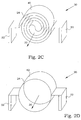
- FIG. 2C another embodiment of a heater microstructure 20 according to the present invention is illustrated.
- the structure is also based on a thin heater sheet structure 24.
- the structure is created in a structure forming a spiral tube shape 40. This enhances the heating of the gas flowing inside the spiral tube 40, thus reducing the heat load on the walls of the stagnation chamber.
- a tube 42 is created by the thin heater sheet structure 24 and provided with electrical connections 32 at opposite ends.
- Such a structure resembles the coil structure used in prior art, giving a similar heat transfer to the gas flow.
- this embodiment has the disadvantage that the thin heater sheet structure 24 has to be created very thin, in order to increase the resistance enough to give reasonable heat dissipation from the tube 42.
- the heater microstructure 20 may be shaped in many other shapes also.
- a common feature is, however, that thin heater sheet structures 24 are used, having a relatively large contact area with the streaming gas.
- the thin heater sheet structure 24 has preferably a width in a direction towards the nozzle exit that is considerably larger, preferably more than at least one order of magnitude larger, than a thickness of the thin heater sheet structure 24.
- the thin heater sheet structures 24 has a core structure 34 of a material based on silicon, e.g. low resistivity silicon or a silicon compound, covered by a thin surface metal or metal compound coating 36.
- Fig. 3 illustrates a flow diagram of main steps of an embodiment of a manufacturing method according to the present invention.
- the procedure starts in step 200.
- a stagnation chamber is provided, and in step 220, a heater microstructure core is manufactured.
- Steps 210 and 220 are preferably performed by MEMS, giving silicon based geometrical structures.
- MEMS microelectrosemiconductor
- other manufacturing approaches according to prior art can also be used with the main principles of present invention, since the particular way in which the stagnation chamber and the heater microstructure core are produced are not of any crucial importance.
- MEMS is traditionally based mainly on single crystalline silicon. The procedures were originally developed by the integrated circuit industry, but due to the attractive patterning properties, mechanical arrangements are easily manufactured by similar processes.
- a typical procedure starts with creating a mask layer on a silicon wafer.
- a photo resist in liquid form is spun onto the wafer.
- the resist is solidified by a soft baking procedure, typically by placing the wafer on a hot plate until the solvent is evaporated.
- the wafer is covered and aligned with a lithography mask having the requested structures, and the wafer is exposed for UV light.
- the photo resist exposed for the UV light changes its properties, while the areas covered by the mask are unchanged.
- the mask is removed and the wafer is developed in a bath with a chemical developer, which removes either the exposed or unexposed areas of the photo resist, depending on the used type.
- the wafer is coated with an etch mask material.
- etching removes silicon that is not covered by the etching mask (and for some methods also some material under the etching mask), and the requested three-dimensional geometrical structures are developed.
- Step 210 is preferably performed by etching two wafers with complementary geometrical cavities. The wafers are thereafter bonded together to form the stagnation chamber as a combined cavity between the wafers. Note, however, that such a method requires that at least step 220 is performed prior to the bonding.
- Step 220 is also preferably performed by means of MEMS.
- MEMS Microelectromechanical System
- other production methods giving similar geometrical structures may be utilized.
- the cross-section pattern of the thin heater sheet structure is thereby provided on the wafer, and the etching is allowed to continue through the entire wafer. In this way, the width of the thin heater sheet structure becomes equal to the original thickness of the silicon wafer. In this way, it is possible to manufacture almost any geometrical structure having a constant cross section along the width of the structure.
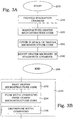
- step 230 the heater microstructure core is covered by a surface metal coating. This can preferably be performed by vacuum deposition techniques, e.g. CVD. One embodiment of step 230 is illustrated in more detail in Fig. 3B .
- the heater microstructure core is heated in step 232. This can be performed in different ways, e.g. by irradiating the heater microstructure core by laser radiation. However, a simple solution is to use the heater microstructure core itself and sending a current through the heater microstructure core, thereby creating resistive heating.
- step 234 gas comprising low quantities of a metal compound is flown over the heater microstructure core.
- step 236 the gas coming into contact with the heated heater microstructure core will decompose, and metal or metal compound will form on the heater microstructure core successively building the surface metal or metal compound coating.
- a metal compound known for metal deposition as such, is W 6 F.
- W 6 F When the tungsten hexaflouride comes into contact with a hot body, in the presence of hydrogen gas, the following reaction takes place: W 6 F + 3 H 2 ⁇ W ( s ) + 6HF ( g )
- wolfram is deposited at the surface, while HF leaves the surface in gaseous state.
- the process becomes more pronounced at higher temperatures, which means that hotter surfaces achieve a thicker deposition.
- a relatively thick deposited metal layer will decrease the local resistance, and the generated heat will thus locally decrease. This is of use during the deposition process, since areas with a thinner coating will be somewhat hotter than areas with thicker coating, which means that the differences in coating thickness will be reduced, since the deposition rate is higher at the hotter spots.
- oxides, nitrides, carbides of W, Ir, Rh, Pd and Pt are possible to use as surface coatings.
- the heater microstructure is in step 240 mounted in the stagnation chamber. (Note here, that if the stagnation chamber is formed by a wafer bonding process as described above, part of step 210 will take place after the mounting of the heater microstructure.) The procedure ends in step 299.
- the surface metal coating step is possible to perform in a dedicated vacuum chamber.
- the covering step 230 can be performed in situ, directly on a heater microstructure core already mounted in the stagnation chamber.
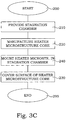
- Fig. 3C illustrates such a method.
- the process begins with the steps 210 and 220 in the same way as in Fig. 3A .
- the step of mounting 240 follows before any surface metal or metal compound coating is performed, i.e. before step 230.
- the stagnation chamber is formed by a wafer bonding process as described above, part of step 210 will take place after the mounting 240 of the heater microstructure in the stagnation chamber.
- the covering step 230 can be performed in situ, inside the stagnation chamber.
- a suitable gas is provided through the inlet to the stagnation chamber, and by connecting a current through the heater microstructure connections, the heater microstructure core is heated, and a deposition takes place.
- This process has certain advantages. First, no separate chambers are needed for the covering process, which saves mounting time and reduces any possibilities to break the relatively fragile heater microstructure cores. Secondly, during the mounting process, the resistance conditions of the connections will always be changed, sometimes more, sometimes less. By monitoring the resistance over the heater microstructure before the covering step, compensations can be made due to the differing contacting resistances. Furthermore, by following the resistance during the deposition, the degree of deposition can be controlled in a very accurate manner by interrupting the heating step or the flowing step, whereby an in situ resistance tuning is achieved. The homogeneity of the surface metal coating is typically not any large problem, due to the self-evening of the coating described above.
- the covering step 230 it would even be possible to etch away at least a part of the silicon or silicon compound forming the heater microstructure core, thus using the silicon or silicon compound merely as a sacrificial structure.
- Fig. 4A illustrates a set-up for metal covering of a heater microstructure core 34 forming a heater microstructure 20.
- the heater microstructure core 34 is mounted in a deposition chamber 50, and connections 54 are connecting the heater microstructure core 34 to a deposition control unit 52 comprising a controlled current source.
- Gas comprising metal compounds is stored in a coating container, in this embodiment a metallizing gas storage 60 and flows 56 into the deposition chamber 50.
- the deposition control unit 52 preferably also comprises functionalities monitoring the development of the resistance over the building-up heater microstructure 20, in order to interrupt the deposition when a suitably thick coating has been achieved.
- Fig. 4B illustrates a set-up for in situ covering of a heater microstructure core 34.
- the deposition chamber 50 is here constituted by the stagnation chamber 12.
- the metallizing gas storage 60 is connected to the inlet pipe 6 via a valve 62. After deposition, the metallizing gas storage 60 can be disconnected. Alternatively, the metallizing gas storage 60 can temporarily replace the gas storage 2, whereby the extra valve 62 can be omitted.
- the deposition control unit 52 may likewise be a separate unit or may include also the heater control unit 22.
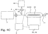
- Fig. 4C illustrates a set-up for in situ covering of a heater microstructure 20, arranged to be operated even in parallel with the ordinary driving operation. Since all parts are present for both covering and driving, such a set-up can be utilized e.g. for performing repairs of the surface metal coating in situ, and even in parallel with or interleaved between operation periods. If a heater microstructure 20 is corroded during use, e.g. due to impurities in the gases used for the driving action, the heater microstructure 20 can in fact be repaired. Metal compound containing gas is flowed through the stagnation chamber 12 while the heater microstructure 20 is heated. Due to the high resistance at spots with thin surface metal coating, these spots becomes hotter and the decomposition of the metal compound occurs faster at these spots, until the requested thickness is regained.
- Fig. 5 illustrates the repair aspect as a flow diagram.
- the procedure starts in step 200.
- step 250 the surface metal coating of the heater microstructure is improved.
- This step in turn comprises the steps 232, 234 and 236, known from Fig. 3B .
- the procedure ends in step 299.
- the resemblance with the original manufacturing is obvious, since it is the result of one and the same inventive idea.
- the gas used in the repair of the heater microstructure can even be further used for driving the gas thruster.
- the container containing driving materia is a conventional gas storage, comprising pressurized gas, e.g. H 2 , He, Ne, N 2 , Ar, Xe, CF 4 , CH 4 , NH 3 , N 2 O, C 3 H 8 or C 4 H 10 , preferably N 2 , Xe, CH 4 , NH 3 or N 2 O.. It is important that the gas is as pure as possible, since even small amounts of impurities may contribute to corrosion of the heater microstructure and stagnation chamber.
- pressurized gas e.g. H 2 , He, Ne, N 2 , Ar, Xe, CF 4 , CH 4 , NH 3 , N 2 O, C 3 H 8 or C 4 H 10 , preferably N 2 , Xe, CH 4 , NH 3 or N 2 O.
- volume reduction is important in space applications, it would be even better to utilise a gas that can be liquidized when exposed to high pressures, e.g. Xe, N 2 O, C 3 H 8 or C 4 H 10 . If the driving material in the container containing driving material is a pressure liquidized gas, the volume is utilised more efficient.
- the driving materia is a compound which exhibits an exothermic reaction and/or a volume expanding reaction when coming into contact with a catalytically active material.
- catalytically active material at the heater microstructure, e.g. as the surface metal coating, the driving gas coming into contact with the heated catalytically active surface will exhibit a reaction, which results in an even increased temperature and/or an increased volume.
- Examples of possible catalytically active materials to use are Pd, Ir, Rh and Pt. In such a way, the driving materia is utilised even more efficient.
- the catalytically active material is exposed not only for the intended driving materia, but also for impurities in the gas and for high temperatures, and is therefore subject for e.g. corrosion and/or evaporation.
- the driving materia could comprise very small amounts of compounds of catalytically active materials. When these compounds are exposed for the hot heater microstructure, they can decompose and the catalytically active material deposits onto the heater microstructure. In this way, new catalytically active material can continuously be provided to the heater microstructure surface.
- the compounds of catalytically active materials are stored in a separate tank and are mixed together with the pure driving materia when needed. If the wear situation of the heater microstructures are well known, it might also be possible to have a common storage of driving materia and the compounds for the heater microstructure.
- a possible candidate for a driving gas is Ni(CO) 4 .
- Fig. 6 illustrates a flow diagram of main steps of an embodiment of a method for operating a gas thruster according to the present invention.
- the procedure starts in step 201, in step 260, gas comprising a compound exhibiting an exothermic reaction when coming into contact with a catalytically active material is released from a container.
- the gas is heated. This heating is performed at least partly by a heater microstructure of silicon or a silicon compound having a surface metal coating of the catalytically active metal. The heating is also at least partly performed by the compound exothermically reacting at the surface metal coating.
- step 280 the heated gas flows through an exit nozzle of the gas thruster, thereby giving rise to a force on the gas thruster in an opposite direction.
- a test equipment of a stagnation chamber 12 with six heater microstructures 20 mounted in series is illustrated.
- the stagnation chamber is produced in a silicon wafer 70.
- the heater microstructures 20 are mounted into grooves 72 in the silicon wafer, where holes in an underlying silicon wafer 70' are provided for the electrical connections (not shown in this Fig.). In such a way, the electrical connection can be provided from the backside of the silicon wafer, external of the stagnation chamber.
- the electrical connection 32 of the heater microstructures 20 is designed as in Fig. 8 .
- the electrical connection 32 has a general elongated form provided with small hooks 74 close to the bottom end.
- the general dimension of the electrical connection 32 is adapted to just fit into a hole 84 in the wafer 70.
- the edges of the hooks 74 are dimensioned for being slightly larger than the hole 84 dimension. In such a way, the electrical connection 32 can be forced through the hole 84, but when the hooks penetrates out from the hole, the edges prohibits the electric connections to be removed again.
- the edges of the hooks 74 rests against an edge 82 of the wafer at the exit of the hole 84. This ensures a mechanical stability.
- the electric connection 32 is manufactured in low-resistance silicon and is therefore conducting.
- the inside surface 78 of the hole 84 as well as areas in the vicinity of the hole openings are oxidized, giving rise to a layer of insulating silicon oxide.
- the wafer is provided with a thin metal layer 86, having a vacuum tight adhesion to the silicon wafer 70.
- a solder material 80 is deposited over the end 76 of the electrical connection 32 and heated until the solder material 80 wets against the end 76 as well as against the thin metal layer 86.
- the heating can be performed by sending an electric current through the thin metal layer 86.
- the adhesion properties can be enhanced by shaping the end 76, e.g. as a sphere as shown in the figure, for providing a geometrical structure that provides enhanced strength to the adhesion to the end 76.
- the orifice of the hole at the bottom side is provided in a recess in the wafer. This makes it possible to contain the entire electrical connection within the main surface plane of the wafer, which reduces risks for mechanical damages.
- electrical vias are typically provided by inserting a metal pin through a hole provided through a wafer.
- the pin is electrically connected at each side of the wafer.
- a via 100 of low-resistance silicon is inserted through a hole 84 an a wafer 70.
- the via 100 has a hook 74 in the vicinity of each end 76 thereof. In this embodiment, there is only one hook at each end, which facilitates the insertion through the hole 84.
- the hole 84 is covered by a silicon oxide layer in order to prohibit electrical shortening towards the wafer 70.
- the wafer presents a recess, in which an edge 82 is provided, against which the hook 74 is intended to rest.
- the recess and an area around the recess is also covered by a metal film 86 assisting in ensuring a good adhesion and a vacuum tight seal.
- the metal film 86 can also be used for heating the solder material when creating the solder, as well as an electrical lead to the via 100 for operational purposes.
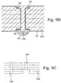
- Fig. 9B the via 100 is inserted through a multiwafer stack 102.
- the retaining structures 74A at one end are small enough to be forced through the hole 84.
- the retaining structures 74B at the other end are larger, ensuring an even more safe mechanical mounting.
- a stack of wafers is shown in cross section.
- a first via 100A is provided through the entire stack, while a second via 100B only passes through three of the wafers.
- One end of the second via 100B thus ends within the stack.
- the solder material for this can be provided through a hole 104, and the final soldering process can be provided by using the metallisation around the via hole 84. It is thus easy also to provide vias between arbitrary planes of the wafer stack by using the present principles.
Landscapes
- Engineering & Computer Science (AREA)
- Chemical & Material Sciences (AREA)
- Combustion & Propulsion (AREA)
- Mechanical Engineering (AREA)
- General Engineering & Computer Science (AREA)
- Nanotechnology (AREA)
- Computer Hardware Design (AREA)
- Health & Medical Sciences (AREA)
- Life Sciences & Earth Sciences (AREA)
- General Health & Medical Sciences (AREA)
- Molecular Biology (AREA)
- Crystallography & Structural Chemistry (AREA)
- Microelectronics & Electronic Packaging (AREA)
- Internal Circuitry In Semiconductor Integrated Circuit Devices (AREA)
- Chemical Vapour Deposition (AREA)
- Remote Sensing (AREA)
- Aviation & Aerospace Engineering (AREA)
- Micromachines (AREA)
- Physical Or Chemical Processes And Apparatus (AREA)
Claims (15)
- Düsenanordnung (10) zur Verwendung in einer Gasschubvorrichtung (1), umfassend.
Stagnationskammer (12) mit einer Eingangsöffnung (7) und einem Düsenauslass (14); und
mindestens eine Heizmikrostruktur (20), die in der Stagnationskammer (12) angeordnet ist,
dadurch gekennzeichnet, dass die mindestens eine Heizmikrostruktur (20) einen Heizmikrostrukturkern (34) aus Silizium oder Siliziumverbindungen umfasst, der mit einer Oberflächenmetall- oder Metallverbindungsbeschichtung (36) überzogen ist. - Düsenanordnung nach Anspruch 1, dadurch gekennzeichnet, dass die Oberflächenmetall- oder Metallverbindungsbeschichtung (36) ein katalytisch aktives Material ist.
- Düsenanordnung nach Anspruch 2, dadurch gekennzeichnet, dass das katalytisch aktive Material ausgewählt ist aus der Liste von: W, Ir, Rh, Pd, Pt und Oxide, Nitride, Carbide von W, Ir, Rh, Pd und Pt.
- Düsenanordnung nach einem der Ansprüche 1 bis 3, dadurch gekennzeichnet, dass die mindestens eine Heizmikrostruktur (20) eine geformte dünne Heizfolienstruktur (24) umfasst.
- Düsenanordnung nach Anspruch 4, dadurch gekennzeichnet, dass die dünne Heizfolienstruktur (24) von dem Düsenauslass (14) aus gesehen mäanderförmig ist.
- Düsenanordnung nach Anspruch 4 oder 5, dadurch gekennzeichnet, dass die dünne Heizfolienstruktur (24) eine Breite in Richtung auf den Düsenauslass (14) aufweist, die wesentlich größer ist als eine Dicke der dünnen Heizfolienstruktur (24).
- Gasschubvorrichtung (1), umfassend:einen Behälter (2), der Schubmaterie enthält;eine Düsenanordnung (10) nach einem der Ansprüche 1 bis 6;eine erste Ventilanordnung (4), die den Behälter (2) und die Düsenanordnung (10) verbindet; undeine Heizsteuereinheit (22), die mit der mindestens einen Heiz-Mikrostruktur (20) verbunden ist.
- Gasschubvorrichtung nach Anspruch 7, dadurch gekennzeichnet, dass die Schubmaterie eine Verbindung ist, die eine exotherme Reaktion aufweist, wenn sie mit einem katalytisch aktiven Material in Kontakt gerät.
- Gasschubvorrichtung nach Anspruch 7 oder 8, dadurch gekennzeichnet, dass die Schubmaterie geringe Mengen einer Verbindung eines katalytisch aktiven Materials umfasst.
- Gasschubvorrichtung nach Anspruch 7 oder 8, dadurch gekennzeichnet, dass sie ferner einen Beschichtungsbehälter (60) umfasst, der eine Verbindung eines katalytisch aktiven Materials umfasst, und eine zweite Ventilanordnung (62), die den Beschichtungsbehälter (60) und die Düsenanordnung (10) verbindet.
- Verfahren zur Herstellung einer Düsenanordnung (10) zur Verwendung in einer Gasschubvorrichtung (1), das folgende Schritte umfasst:Bereitstellen (210) einer Stagnationskammer (12) mit einer Eingangsöffnung (7) und einem Düsenauslass (14);Herstellen (220) eines Heiz-Mikrostrukturkerns (34) aus Silizium oder einer Siliziumverbindung;Bedecken (230) einer Fläche des Heiz-Mikrostrukturkerns (34) mit einer Oberflächenmetall- oder Metallverbindungsbeschichtung (36);wobei der Schritt des Bedeckens (230) wiederum folgende Schritte umfasst:Erhitzen (232) des Heiz-Mikrostrukturkerns (34) durch das Durchleiten von elektrischem Strom;Strömen (234) eines Gases, das geringe Mengen einer Metallverbindung umfasst, über den HeizMikrostrukturkern (34); undAufspalten (236) der Verbindung in dem erhitzten HeizMikrostrukturkern (34) in das Metall oder die Metallverbindung (36); undAufstellen (240) der Heiz-Mikrostruktur in der Stagnationskammer (12).
- Verfahren nach Anspruch 11, dadurch gekennzeichnet, dass der Schritt des Aufstellens (240) vor dem Schritt des Bedeckens (230) erfolgt, wobei der Schritt des Bedeckens (230) in situ in der Stagnationskammer (12) ausgeführt wird.
- Verfahren nach Anspruch 12, dadurch gekennzeichnet, dass der Schritt des Bedeckens (230) folgende weitere Schritte umfasst:Überwachen eines Widerstandes über die Heiz-Mikrostruktur (20); und Unterbrechen von mindestens einem des Schritts des Erhitzens (232) und des Schritts des Strömens (234), wodurch eine Einstellung der in situ-Resistenz erreicht wird.
- Verfahren zur In situ-Reparatur einer Düsenanordnung (10) zur Verwendung in einer Gasschubvorrichtung (1), wobei die Düsenanordnung (10) mindestens eine Heiz-Mikrostruktur (20) umfasst, die aus Silizium oder einer Siliziumverbindung mit einer Oberflächenmetall- oder Metallverbindungsbeschichtung (36) besteht und die in einer Stagnationskammer (12) angeordnet ist, wobei das Verfahren folgenden Schritt aufweist:Reparieren (250) der Heiz-Mikrostruktur (20) durch Verbesserung der Oberflächenmetall- oder Metallverbindungsbeschichtung (36);wobei der Schritt des Reparierens (250) wiederum folgende Schritte umfasst:Erhitzen (232) der Heiz-Mikrostruktur (20) durch das Durchleiten von elektrischem Strom;Strömen (234) eines Gases, das geringe Mengen einer Metallverbindung umfasst, welche das Metall oder die Metallverbindung umfasst, über die Heiz-Mikrostruktur (20); undAufspalten (236) der Verbindung in der erhitzten Heiz-Mikrostruktur (20) in das Metall oder die Metallverbindung (36).
- Verfahren zum Betrieb einer Gasschubvorrichtung (1), das folgende Schritte umfasst:Abgeben (260) von Gas aus einem Behälter (2);Erhitzen (270) des Gases; undStrömen (280) des erhitzten Gases durch eine Auslassdüse (14) der Gasschubvorrichtung (1), dadurch gekennzeichnet, dassdas Gas eine Verbindung umfasst, die eine exotherme Reaktion aufweist, wenn sie mit einem katalytisch aktiven Material in Kontakt gerät;wobei der Schritt des Erhitzens (270) von einer Heiz-Mikrostruktur (20) aus Silizium- oder einer Siliziumverbindung mit einer Oberflächenmetall- oder Metallverbindungsbeschichtung (36) des katalytisch aktiven Metalls ausgeführt wird,wobei der Schritt des Erhitzens (280) des Gases mindestens teilweise von der auf der Oberflächenmetall- oder Metallverbindungsbeschichtung (36) exothermisch reagierenden Verbindung ausgeführt wird.
Applications Claiming Priority (2)
| Application Number | Priority Date | Filing Date | Title |
|---|---|---|---|
| SE0601832A SE530415C2 (sv) | 2006-09-04 | 2006-09-04 | Gastrustor |
| PCT/SE2007/050615 WO2008030175A1 (en) | 2006-09-04 | 2007-09-04 | Nozzle arrangement for use in a gas thruster, gas thruster, method for manufacturing a nozzle arrangement, method for in-situ repairing of a nozzle arrangement and a method for operating a gas thrusters |
Publications (3)
| Publication Number | Publication Date |
|---|---|
| EP2064436A1 EP2064436A1 (de) | 2009-06-03 |
| EP2064436A4 EP2064436A4 (de) | 2015-03-04 |
| EP2064436B1 true EP2064436B1 (de) | 2016-04-06 |
Family
ID=39157508
Family Applications (2)
| Application Number | Title | Priority Date | Filing Date |
|---|---|---|---|
| EP07794220.9A Not-in-force EP2064436B1 (de) | 2006-09-04 | 2007-09-04 | Düsenanordnung zur verwendung in einer gasschubvorrichtung, gasschubvorrichtung, verfahren zur herstellung einer düsenanordnung, verfahren zur in-situ-reparatur einer düsenanordnung und verfahren zum betrieb einer gasschubvorrichtung |
| EP07794222.5A Not-in-force EP2067391B1 (de) | 2006-09-04 | 2007-09-04 | Substratdurchdringende elektrische verbindungen |
Family Applications After (1)
| Application Number | Title | Priority Date | Filing Date |
|---|---|---|---|
| EP07794222.5A Not-in-force EP2067391B1 (de) | 2006-09-04 | 2007-09-04 | Substratdurchdringende elektrische verbindungen |
Country Status (4)
| Country | Link |
|---|---|
| US (2) | US8336314B2 (de) |
| EP (2) | EP2064436B1 (de) |
| SE (1) | SE530415C2 (de) |
| WO (2) | WO2008030175A1 (de) |
Families Citing this family (10)
| Publication number | Priority date | Publication date | Assignee | Title |
|---|---|---|---|---|
| JP2009064908A (ja) * | 2007-09-05 | 2009-03-26 | Ibiden Co Ltd | 配線基板およびその製造方法 |
| US8865354B2 (en) * | 2010-03-30 | 2014-10-21 | West Virginia University | Inorganic solid electrolyte glass phase composite and a battery containing an inorganic solid electrolyte glass phase composite |
| JP6046645B2 (ja) | 2011-03-02 | 2016-12-21 | ゲーム・チェンジャーズ・リミテッド・ライアビリティ・カンパニーGame Changers, Llc | 分散型マイクロクラスタのための耐故障性制御システム |
| DE102012102533B3 (de) * | 2012-03-23 | 2013-08-22 | Infineon Technologies Austria Ag | Integrierte Leistungstransistorschaltung mit Strommesszelle und Verfahren zu deren Herstellung sowie eine Anordnung diese enthaltend |
| EP2861859B1 (de) * | 2012-06-15 | 2018-03-21 | Game Changers, Llc | Verwendungen eines microthrusters und verbesserungen daran |
| US8877137B2 (en) | 2012-12-03 | 2014-11-04 | Intelligent Energy Inc. | Hydrogen generator |
| US9768147B2 (en) | 2014-02-03 | 2017-09-19 | Micron Technology, Inc. | Thermal pads between stacked semiconductor dies and associated systems and methods |
| CN104409364B (zh) * | 2014-11-19 | 2017-12-01 | 清华大学 | 转接板及其制作方法、封装结构及用于转接板的键合方法 |
| JP6492768B2 (ja) * | 2015-02-27 | 2019-04-03 | 富士通株式会社 | 電子装置及びはんだ実装方法 |
| US10889389B2 (en) * | 2017-04-26 | 2021-01-12 | Marotta Controls, Inc. | Electronic pressure regulation system with proportional control valve |
Family Cites Families (42)
| Publication number | Priority date | Publication date | Assignee | Title |
|---|---|---|---|---|
| US1967757A (en) * | 1932-02-10 | 1934-07-24 | Joseph S Losee | Fan heater |
| US2988430A (en) * | 1958-02-11 | 1961-06-13 | Thompson Ramo Wooldridge Inc | Fuel dissociation chamber |
| US3846741A (en) * | 1973-09-25 | 1974-11-05 | Amp Inc | Circuit board post type terminal |
| US4220846A (en) * | 1978-07-26 | 1980-09-02 | The Fluorocarbon Company | Method and apparatus utilizing a porous vitreous carbon body particularly for fluid heating |
| US4394712A (en) * | 1981-03-18 | 1983-07-19 | General Electric Company | Alignment-enhancing feed-through conductors for stackable silicon-on-sapphire wafers |
| US4523429A (en) * | 1983-04-01 | 1985-06-18 | Rca Corporation | Cold start surge current limiting system for a hydrazine thruster augmentation heater |
| US4620415A (en) * | 1983-09-29 | 1986-11-04 | Rocket Research Company | Method for initiating decomposition of hydrazine fuels |
| JPS6244971A (ja) * | 1985-08-23 | 1987-02-26 | 日本特殊陶業株式会社 | セラミツク基板ヒ−タ− |
| FI78784C (fi) * | 1988-01-18 | 1989-09-11 | Vaisala Oy | Tryckgivarkonstruktion och foerfarande foer framstaellning daerav. |
| US5431737A (en) * | 1992-02-04 | 1995-07-11 | Genus, Inc. | Interchangeable CVD chuck surface |
| US5365790A (en) | 1992-04-02 | 1994-11-22 | Motorola, Inc. | Device with bonded conductive and insulating substrates and method therefore |
| US5519191A (en) * | 1992-10-30 | 1996-05-21 | Corning Incorporated | Fluid heater utilizing laminar heating element having conductive layer bonded to flexible ceramic foil substrate |
| US6107109A (en) * | 1997-12-18 | 2000-08-22 | Micron Technology, Inc. | Method for fabricating a semiconductor interconnect with laser machined electrical paths through substrate |
| US6208156B1 (en) * | 1998-09-03 | 2001-03-27 | Micron Technology, Inc. | Test carrier for packaging semiconductor components having contact balls and calibration carrier for calibrating semiconductor test systems |
| JP3249496B2 (ja) * | 1998-11-10 | 2002-01-21 | 株式会社東芝 | 半導体装置及び半導体装置の製造方法 |
| IL128206A0 (en) * | 1999-01-24 | 1999-11-30 | Yissum Res Dev Co | A process for the epoxidation of alkenes and polyoxofluorometalates for use therein |
| JP4097431B2 (ja) * | 1999-09-17 | 2008-06-11 | 松下電器産業株式会社 | 高分子電解質型燃料電池 |
| FR2805709B1 (fr) * | 2000-02-28 | 2002-05-17 | Commissariat Energie Atomique | Connexion electrique entre deux faces d'un substrat et procede de realisation |
| US6516604B2 (en) * | 2000-03-27 | 2003-02-11 | California Institute Of Technology | Micro-colloid thruster system |
| US6577013B1 (en) * | 2000-09-05 | 2003-06-10 | Amkor Technology, Inc. | Chip size semiconductor packages with stacked dies |
| US6779335B2 (en) * | 2000-12-07 | 2004-08-24 | Joseph Roger Herdy, Jr. | Burning nitrous oxide and a fuel |
| US6908873B2 (en) * | 2000-12-22 | 2005-06-21 | Headwaters Nanokinetix, Inc. | Regeneration of spent supported metal catalysts |
| JP2002270718A (ja) * | 2001-03-07 | 2002-09-20 | Seiko Epson Corp | 配線基板及びその製造方法、半導体装置及びその製造方法、回路基板並びに電子機器 |
| US6494402B2 (en) * | 2001-05-14 | 2002-12-17 | The Aerospace Corporation | Lateral exhaust microthruster |
| US20040031885A1 (en) * | 2001-07-30 | 2004-02-19 | D'ausilio Robert F. | In orbit space transportation & recovery system |
| US6848177B2 (en) * | 2002-03-28 | 2005-02-01 | Intel Corporation | Integrated circuit die and an electronic assembly having a three-dimensional interconnection scheme |
| US6716737B2 (en) * | 2002-07-29 | 2004-04-06 | Hewlett-Packard Development Company, L.P. | Method of forming a through-substrate interconnect |
| SE527154C2 (sv) * | 2002-09-09 | 2006-01-10 | Nanospace Ab | Intern gasvärmare för mikroframdrivning |
| WO2004098994A2 (en) * | 2002-12-13 | 2004-11-18 | Arizona Board Of Regents | Attitude determination and control system for a solar sail spacecraft |
| GB2396595A (en) * | 2002-12-23 | 2004-06-30 | Astrium Ltd | A secondary payload satellite |
| US6979805B2 (en) * | 2003-01-08 | 2005-12-27 | Hewlett-Packard Development Company, L.P. | Fuel-cell resistors and methods |
| US6982565B2 (en) * | 2003-03-06 | 2006-01-03 | Micron Technology, Inc. | Test system and test method with interconnect having semiconductor spring contacts |
| SE526366C3 (sv) * | 2003-03-21 | 2005-10-26 | Silex Microsystems Ab | Elektriska anslutningar i substrat |
| JP3972846B2 (ja) * | 2003-03-25 | 2007-09-05 | セイコーエプソン株式会社 | 半導体装置の製造方法 |
| US8084866B2 (en) * | 2003-12-10 | 2011-12-27 | Micron Technology, Inc. | Microelectronic devices and methods for filling vias in microelectronic devices |
| IL159248A (en) * | 2003-12-08 | 2011-10-31 | Aharon Oren | Impulse motor with increased electro-thermal impulse |
| US6943106B1 (en) * | 2004-02-20 | 2005-09-13 | Micron Technology, Inc. | Methods of fabricating interconnects for semiconductor components including plating solder-wetting material and solder filling |
| US6996972B2 (en) * | 2004-05-18 | 2006-02-14 | The Boeing Company | Method of ionizing a liquid propellant and an electric thruster implementing such a method |
| US7109068B2 (en) * | 2004-08-31 | 2006-09-19 | Micron Technology, Inc. | Through-substrate interconnect fabrication methods |
| US7300857B2 (en) * | 2004-09-02 | 2007-11-27 | Micron Technology, Inc. | Through-wafer interconnects for photoimager and memory wafers |
| KR100704971B1 (ko) * | 2005-01-21 | 2007-04-10 | 타이코에이엠피 주식회사 | 무납땜 연결 구조를 갖는 더블 인쇄회로기판 |
| US20060290001A1 (en) * | 2005-06-28 | 2006-12-28 | Micron Technology, Inc. | Interconnect vias and associated methods of formation |
-
2006
- 2006-09-04 SE SE0601832A patent/SE530415C2/sv not_active IP Right Cessation
-
2007
- 2007-09-04 US US12/439,749 patent/US8336314B2/en not_active Expired - Fee Related
- 2007-09-04 WO PCT/SE2007/050615 patent/WO2008030175A1/en not_active Ceased
- 2007-09-04 EP EP07794220.9A patent/EP2064436B1/de not_active Not-in-force
- 2007-09-04 EP EP07794222.5A patent/EP2067391B1/de not_active Not-in-force
- 2007-09-04 WO PCT/SE2007/050617 patent/WO2008030176A1/en not_active Ceased
- 2007-09-04 US US12/439,568 patent/US8395057B2/en not_active Expired - Fee Related
Also Published As
| Publication number | Publication date |
|---|---|
| EP2067391B1 (de) | 2017-03-01 |
| WO2008030176A1 (en) | 2008-03-13 |
| SE530415C2 (sv) | 2008-05-27 |
| US8395057B2 (en) | 2013-03-12 |
| US8336314B2 (en) | 2012-12-25 |
| US20100139239A1 (en) | 2010-06-10 |
| EP2064436A4 (de) | 2015-03-04 |
| EP2064436A1 (de) | 2009-06-03 |
| EP2067391A1 (de) | 2009-06-10 |
| EP2067391A4 (de) | 2014-05-07 |
| SE0601832L (sv) | 2008-03-05 |
| WO2008030175A1 (en) | 2008-03-13 |
| US20100018764A1 (en) | 2010-01-28 |
Similar Documents
| Publication | Publication Date | Title |
|---|---|---|
| US8336314B2 (en) | Method of manufacturing a nozzle arrangement and method for in-situ repairing a nozzle arrangement | |
| US7732086B2 (en) | Bonded polyimide fuel cell package | |
| JP2004537425A (ja) | 熱効率にすぐれるマイクロマシンデバイス | |
| KR20040104382A (ko) | 반응장치와 그 제조방법, 개질장치, 전원공급시스템 | |
| KR100649374B1 (ko) | 미소 구성품의 제조방법 | |
| Pugia et al. | Characterization of film-evaporating microcapillaries for water-based microthrusters | |
| US20080173354A1 (en) | Micro-machined temperature dependent one-shot valve and process for production thereof | |
| JP4580664B2 (ja) | マイクロリアクターおよびその製造方法 | |
| WO2004069738A1 (ja) | マイクロリアクターおよびその製造方法 | |
| TWI357675B (de) | ||
| US8109769B1 (en) | Micromachined flex interposers | |
| JP2004082733A (ja) | 先細熱的アクチュエータ | |
| JP4909887B2 (ja) | 高圧毛細管マイクロ流体バルブ装置およびその製造方法 | |
| WO2006023979A2 (en) | Water heater and method of providing the same | |
| US6533951B1 (en) | Method of manufacturing fluid pump | |
| US20060105912A1 (en) | Microstructured catalyst body and method for production thereof | |
| JP2023550513A (ja) | 流体流を加熱するための電気加熱システム | |
| TWI248877B (en) | Method for fabricating a monolithic fluid eject device | |
| CN112960642B (zh) | 一种用于高温加热的金属线结构的制备方法 | |
| KR100385969B1 (ko) | 복수층의 형상기억합금을 이용한 잉크젯 프린터 헤드용 마이크로 액츄에이터 및 그 제조방법 | |
| CN122009530A (zh) | 一种微型推进器及其制备方法 | |
| Pennarun et al. | MEMS Based One Shot Electro-Thermal Micro-Switches for System Reconfiguration | |
| Tiggelaar et al. | Silicon-based microreactors as research tools in chemistry | |
| TWI492852B (zh) | 抗龜裂之熱彎曲致動器 | |
| SE527154C2 (sv) | Intern gasvärmare för mikroframdrivning |
Legal Events
| Date | Code | Title | Description |
|---|---|---|---|
| PUAI | Public reference made under article 153(3) epc to a published international application that has entered the european phase |
Free format text: ORIGINAL CODE: 0009012 |
|
| 17P | Request for examination filed |
Effective date: 20090330 |
|
| AK | Designated contracting states |
Kind code of ref document: A1 Designated state(s): AT BE BG CH CY CZ DE DK EE ES FI FR GB GR HU IE IS IT LI LT LU LV MC MT NL PL PT RO SE SI SK TR |
|
| AX | Request for extension of the european patent |
Extension state: AL BA HR MK RS |
|
| RIN1 | Information on inventor provided before grant (corrected) |
Inventor name: JOHANSSON, HAKAN Inventor name: GROENLAND, TOR-ARNE Inventor name: RANGSTEN, PELLE Inventor name: BEJHED, JOHAN |
|
| DAX | Request for extension of the european patent (deleted) | ||
| REG | Reference to a national code |
Ref country code: DE Ref legal event code: R079 Ref document number: 602007045670 Country of ref document: DE Free format text: PREVIOUS MAIN CLASS: F02K0009620000 Ipc: H05K0003360000 |
|
| A4 | Supplementary search report drawn up and despatched |
Effective date: 20150203 |
|
| RIC1 | Information provided on ipc code assigned before grant |
Ipc: B81B 7/00 20060101ALI20150128BHEP Ipc: B64G 1/10 20060101ALI20150128BHEP Ipc: F02K 9/62 20060101ALI20150128BHEP Ipc: B82Y 15/00 20110101ALI20150128BHEP Ipc: B64G 1/26 20060101ALI20150128BHEP Ipc: H05K 3/36 20060101AFI20150128BHEP Ipc: F02K 9/80 20060101ALI20150128BHEP Ipc: B64G 1/40 20060101ALI20150128BHEP Ipc: H01L 23/48 20060101ALI20150128BHEP |
|
| GRAP | Despatch of communication of intention to grant a patent |
Free format text: ORIGINAL CODE: EPIDOSNIGR1 |
|
| INTG | Intention to grant announced |
Effective date: 20150909 |
|
| GRAS | Grant fee paid |
Free format text: ORIGINAL CODE: EPIDOSNIGR3 |
|
| RIN1 | Information on inventor provided before grant (corrected) |
Inventor name: RANGSTEN, PELLE Inventor name: JOHANSSON, HAKAN Inventor name: BEJHED, JOHAN Inventor name: GROENLAND, TOR-ARNE |
|
| GRAA | (expected) grant |
Free format text: ORIGINAL CODE: 0009210 |
|
| AK | Designated contracting states |
Kind code of ref document: B1 Designated state(s): AT BE BG CH CY CZ DE DK EE ES FI FR GB GR HU IE IS IT LI LT LU LV MC MT NL PL PT RO SE SI SK TR |
|
| REG | Reference to a national code |
Ref country code: GB Ref legal event code: FG4D |
|
| REG | Reference to a national code |
Ref country code: AT Ref legal event code: REF Ref document number: 789020 Country of ref document: AT Kind code of ref document: T Effective date: 20160415 Ref country code: CH Ref legal event code: EP |
|
| REG | Reference to a national code |
Ref country code: IE Ref legal event code: FG4D |
|
| REG | Reference to a national code |
Ref country code: DE Ref legal event code: R096 Ref document number: 602007045670 Country of ref document: DE |
|
| REG | Reference to a national code |
Ref country code: LT Ref legal event code: MG4D Ref country code: NL Ref legal event code: MP Effective date: 20160406 |
|
| REG | Reference to a national code |
Ref country code: AT Ref legal event code: MK05 Ref document number: 789020 Country of ref document: AT Kind code of ref document: T Effective date: 20160406 |
|
| REG | Reference to a national code |
Ref country code: FR Ref legal event code: PLFP Year of fee payment: 10 |
|
| PG25 | Lapsed in a contracting state [announced via postgrant information from national office to epo] |
Ref country code: NL Free format text: LAPSE BECAUSE OF FAILURE TO SUBMIT A TRANSLATION OF THE DESCRIPTION OR TO PAY THE FEE WITHIN THE PRESCRIBED TIME-LIMIT Effective date: 20160406 |
|
| PG25 | Lapsed in a contracting state [announced via postgrant information from national office to epo] |
Ref country code: IS Free format text: LAPSE BECAUSE OF FAILURE TO SUBMIT A TRANSLATION OF THE DESCRIPTION OR TO PAY THE FEE WITHIN THE PRESCRIBED TIME-LIMIT Effective date: 20160806 Ref country code: PL Free format text: LAPSE BECAUSE OF FAILURE TO SUBMIT A TRANSLATION OF THE DESCRIPTION OR TO PAY THE FEE WITHIN THE PRESCRIBED TIME-LIMIT Effective date: 20160406 Ref country code: LT Free format text: LAPSE BECAUSE OF FAILURE TO SUBMIT A TRANSLATION OF THE DESCRIPTION OR TO PAY THE FEE WITHIN THE PRESCRIBED TIME-LIMIT Effective date: 20160406 Ref country code: FI Free format text: LAPSE BECAUSE OF FAILURE TO SUBMIT A TRANSLATION OF THE DESCRIPTION OR TO PAY THE FEE WITHIN THE PRESCRIBED TIME-LIMIT Effective date: 20160406 |
|
| PG25 | Lapsed in a contracting state [announced via postgrant information from national office to epo] |
Ref country code: SE Free format text: LAPSE BECAUSE OF FAILURE TO SUBMIT A TRANSLATION OF THE DESCRIPTION OR TO PAY THE FEE WITHIN THE PRESCRIBED TIME-LIMIT Effective date: 20160406 Ref country code: LV Free format text: LAPSE BECAUSE OF FAILURE TO SUBMIT A TRANSLATION OF THE DESCRIPTION OR TO PAY THE FEE WITHIN THE PRESCRIBED TIME-LIMIT Effective date: 20160406 Ref country code: GR Free format text: LAPSE BECAUSE OF FAILURE TO SUBMIT A TRANSLATION OF THE DESCRIPTION OR TO PAY THE FEE WITHIN THE PRESCRIBED TIME-LIMIT Effective date: 20160707 Ref country code: AT Free format text: LAPSE BECAUSE OF FAILURE TO SUBMIT A TRANSLATION OF THE DESCRIPTION OR TO PAY THE FEE WITHIN THE PRESCRIBED TIME-LIMIT Effective date: 20160406 Ref country code: PT Free format text: LAPSE BECAUSE OF FAILURE TO SUBMIT A TRANSLATION OF THE DESCRIPTION OR TO PAY THE FEE WITHIN THE PRESCRIBED TIME-LIMIT Effective date: 20160808 Ref country code: ES Free format text: LAPSE BECAUSE OF FAILURE TO SUBMIT A TRANSLATION OF THE DESCRIPTION OR TO PAY THE FEE WITHIN THE PRESCRIBED TIME-LIMIT Effective date: 20160406 |
|
| PG25 | Lapsed in a contracting state [announced via postgrant information from national office to epo] |
Ref country code: BE Free format text: LAPSE BECAUSE OF FAILURE TO SUBMIT A TRANSLATION OF THE DESCRIPTION OR TO PAY THE FEE WITHIN THE PRESCRIBED TIME-LIMIT Effective date: 20160406 Ref country code: IT Free format text: LAPSE BECAUSE OF FAILURE TO SUBMIT A TRANSLATION OF THE DESCRIPTION OR TO PAY THE FEE WITHIN THE PRESCRIBED TIME-LIMIT Effective date: 20160406 |
|
| REG | Reference to a national code |
Ref country code: DE Ref legal event code: R097 Ref document number: 602007045670 Country of ref document: DE |
|
| PG25 | Lapsed in a contracting state [announced via postgrant information from national office to epo] |
Ref country code: CZ Free format text: LAPSE BECAUSE OF FAILURE TO SUBMIT A TRANSLATION OF THE DESCRIPTION OR TO PAY THE FEE WITHIN THE PRESCRIBED TIME-LIMIT Effective date: 20160406 Ref country code: SK Free format text: LAPSE BECAUSE OF FAILURE TO SUBMIT A TRANSLATION OF THE DESCRIPTION OR TO PAY THE FEE WITHIN THE PRESCRIBED TIME-LIMIT Effective date: 20160406 Ref country code: RO Free format text: LAPSE BECAUSE OF FAILURE TO SUBMIT A TRANSLATION OF THE DESCRIPTION OR TO PAY THE FEE WITHIN THE PRESCRIBED TIME-LIMIT Effective date: 20160406 Ref country code: EE Free format text: LAPSE BECAUSE OF FAILURE TO SUBMIT A TRANSLATION OF THE DESCRIPTION OR TO PAY THE FEE WITHIN THE PRESCRIBED TIME-LIMIT Effective date: 20160406 Ref country code: DK Free format text: LAPSE BECAUSE OF FAILURE TO SUBMIT A TRANSLATION OF THE DESCRIPTION OR TO PAY THE FEE WITHIN THE PRESCRIBED TIME-LIMIT Effective date: 20160406 |
|
| PLBE | No opposition filed within time limit |
Free format text: ORIGINAL CODE: 0009261 |
|
| STAA | Information on the status of an ep patent application or granted ep patent |
Free format text: STATUS: NO OPPOSITION FILED WITHIN TIME LIMIT |
|
| 26N | No opposition filed |
Effective date: 20170110 |
|
| PG25 | Lapsed in a contracting state [announced via postgrant information from national office to epo] |
Ref country code: MC Free format text: LAPSE BECAUSE OF FAILURE TO SUBMIT A TRANSLATION OF THE DESCRIPTION OR TO PAY THE FEE WITHIN THE PRESCRIBED TIME-LIMIT Effective date: 20160406 |
|
| REG | Reference to a national code |
Ref country code: CH Ref legal event code: PL |
|
| PG25 | Lapsed in a contracting state [announced via postgrant information from national office to epo] |
Ref country code: SI Free format text: LAPSE BECAUSE OF FAILURE TO SUBMIT A TRANSLATION OF THE DESCRIPTION OR TO PAY THE FEE WITHIN THE PRESCRIBED TIME-LIMIT Effective date: 20160406 |
|
| REG | Reference to a national code |
Ref country code: IE Ref legal event code: MM4A |
|
| PG25 | Lapsed in a contracting state [announced via postgrant information from national office to epo] |
Ref country code: LI Free format text: LAPSE BECAUSE OF NON-PAYMENT OF DUE FEES Effective date: 20160930 Ref country code: IE Free format text: LAPSE BECAUSE OF NON-PAYMENT OF DUE FEES Effective date: 20160904 Ref country code: CH Free format text: LAPSE BECAUSE OF NON-PAYMENT OF DUE FEES Effective date: 20160930 |
|
| PG25 | Lapsed in a contracting state [announced via postgrant information from national office to epo] |
Ref country code: LU Free format text: LAPSE BECAUSE OF NON-PAYMENT OF DUE FEES Effective date: 20160904 |
|
| REG | Reference to a national code |
Ref country code: FR Ref legal event code: PLFP Year of fee payment: 11 |
|
| PG25 | Lapsed in a contracting state [announced via postgrant information from national office to epo] |
Ref country code: HU Free format text: LAPSE BECAUSE OF FAILURE TO SUBMIT A TRANSLATION OF THE DESCRIPTION OR TO PAY THE FEE WITHIN THE PRESCRIBED TIME-LIMIT; INVALID AB INITIO Effective date: 20070904 Ref country code: CY Free format text: LAPSE BECAUSE OF FAILURE TO SUBMIT A TRANSLATION OF THE DESCRIPTION OR TO PAY THE FEE WITHIN THE PRESCRIBED TIME-LIMIT Effective date: 20160406 |
|
| PG25 | Lapsed in a contracting state [announced via postgrant information from national office to epo] |
Ref country code: TR Free format text: LAPSE BECAUSE OF FAILURE TO SUBMIT A TRANSLATION OF THE DESCRIPTION OR TO PAY THE FEE WITHIN THE PRESCRIBED TIME-LIMIT Effective date: 20160406 Ref country code: MT Free format text: LAPSE BECAUSE OF NON-PAYMENT OF DUE FEES Effective date: 20160930 |
|
| PG25 | Lapsed in a contracting state [announced via postgrant information from national office to epo] |
Ref country code: BG Free format text: LAPSE BECAUSE OF FAILURE TO SUBMIT A TRANSLATION OF THE DESCRIPTION OR TO PAY THE FEE WITHIN THE PRESCRIBED TIME-LIMIT Effective date: 20160406 |
|
| REG | Reference to a national code |
Ref country code: FR Ref legal event code: PLFP Year of fee payment: 12 |
|
| PGFP | Annual fee paid to national office [announced via postgrant information from national office to epo] |
Ref country code: DE Payment date: 20190920 Year of fee payment: 13 Ref country code: FR Payment date: 20190920 Year of fee payment: 13 |
|
| PGFP | Annual fee paid to national office [announced via postgrant information from national office to epo] |
Ref country code: GB Payment date: 20190913 Year of fee payment: 13 |
|
| REG | Reference to a national code |
Ref country code: DE Ref legal event code: R119 Ref document number: 602007045670 Country of ref document: DE |
|
| GBPC | Gb: european patent ceased through non-payment of renewal fee |
Effective date: 20200904 |
|
| PG25 | Lapsed in a contracting state [announced via postgrant information from national office to epo] |
Ref country code: FR Free format text: LAPSE BECAUSE OF NON-PAYMENT OF DUE FEES Effective date: 20200930 Ref country code: DE Free format text: LAPSE BECAUSE OF NON-PAYMENT OF DUE FEES Effective date: 20210401 |
|
| PG25 | Lapsed in a contracting state [announced via postgrant information from national office to epo] |
Ref country code: GB Free format text: LAPSE BECAUSE OF NON-PAYMENT OF DUE FEES Effective date: 20200904 |