EP2064785B1 - Vernierabgestimmte koppelresonator-ld mit einem stegwellenleiter mit leerstellen zur unterdrückung von longitudinalen moden - Google Patents
Vernierabgestimmte koppelresonator-ld mit einem stegwellenleiter mit leerstellen zur unterdrückung von longitudinalen moden Download PDFInfo
- Publication number
- EP2064785B1 EP2064785B1 EP07805475.6A EP07805475A EP2064785B1 EP 2064785 B1 EP2064785 B1 EP 2064785B1 EP 07805475 A EP07805475 A EP 07805475A EP 2064785 B1 EP2064785 B1 EP 2064785B1
- Authority
- EP
- European Patent Office
- Prior art keywords
- refractive index
- slots
- ridge
- altering
- laser device
- Prior art date
- Legal status (The legal status is an assumption and is not a legal conclusion. Google has not performed a legal analysis and makes no representation as to the accuracy of the status listed.)
- Not-in-force
Links
- 230000001629 suppression Effects 0.000 title description 12
- 238000001228 spectrum Methods 0.000 claims description 50
- 238000005086 pumping Methods 0.000 claims description 33
- 238000004519 manufacturing process Methods 0.000 claims description 13
- 239000000463 material Substances 0.000 claims description 13
- 239000004065 semiconductor Substances 0.000 claims description 10
- 238000000034 method Methods 0.000 claims description 9
- 238000004891 communication Methods 0.000 claims description 2
- 238000002310 reflectometry Methods 0.000 description 30
- 238000005253 cladding Methods 0.000 description 22
- 230000003287 optical effect Effects 0.000 description 12
- 230000008859 change Effects 0.000 description 7
- 230000008569 process Effects 0.000 description 7
- 230000005540 biological transmission Effects 0.000 description 6
- 230000014509 gene expression Effects 0.000 description 6
- 235000008694 Humulus lupulus Nutrition 0.000 description 4
- 230000000694 effects Effects 0.000 description 4
- 238000000295 emission spectrum Methods 0.000 description 4
- 230000001965 increasing effect Effects 0.000 description 4
- 238000002347 injection Methods 0.000 description 4
- 239000007924 injection Substances 0.000 description 4
- 230000008901 benefit Effects 0.000 description 3
- 238000010276 construction Methods 0.000 description 3
- 238000001514 detection method Methods 0.000 description 3
- 230000004044 response Effects 0.000 description 3
- 230000003595 spectral effect Effects 0.000 description 3
- 238000012512 characterization method Methods 0.000 description 2
- 238000009826 distribution Methods 0.000 description 2
- 239000002019 doping agent Substances 0.000 description 2
- 239000000835 fiber Substances 0.000 description 2
- 238000005259 measurement Methods 0.000 description 2
- 239000002096 quantum dot Substances 0.000 description 2
- 238000000862 absorption spectrum Methods 0.000 description 1
- 230000009471 action Effects 0.000 description 1
- 238000004458 analytical method Methods 0.000 description 1
- 239000000470 constituent Substances 0.000 description 1
- 238000007796 conventional method Methods 0.000 description 1
- 230000008878 coupling Effects 0.000 description 1
- 238000010168 coupling process Methods 0.000 description 1
- 238000005859 coupling reaction Methods 0.000 description 1
- 230000007423 decrease Effects 0.000 description 1
- 230000003247 decreasing effect Effects 0.000 description 1
- 230000007547 defect Effects 0.000 description 1
- 238000001312 dry etching Methods 0.000 description 1
- 230000002708 enhancing effect Effects 0.000 description 1
- 238000005530 etching Methods 0.000 description 1
- 238000001914 filtration Methods 0.000 description 1
- 238000002955 isolation Methods 0.000 description 1
- 239000011159 matrix material Substances 0.000 description 1
- 239000002184 metal Substances 0.000 description 1
- 239000013307 optical fiber Substances 0.000 description 1
- 230000010363 phase shift Effects 0.000 description 1
- 238000000206 photolithography Methods 0.000 description 1
- 238000000985 reflectance spectrum Methods 0.000 description 1
- 238000000926 separation method Methods 0.000 description 1
- 239000000243 solution Substances 0.000 description 1
- 230000002269 spontaneous effect Effects 0.000 description 1
Images





Classifications
-
- H—ELECTRICITY
- H01—ELECTRIC ELEMENTS
- H01S—DEVICES USING THE PROCESS OF LIGHT AMPLIFICATION BY STIMULATED EMISSION OF RADIATION [LASER] TO AMPLIFY OR GENERATE LIGHT; DEVICES USING STIMULATED EMISSION OF ELECTROMAGNETIC RADIATION IN WAVE RANGES OTHER THAN OPTICAL
- H01S5/00—Semiconductor lasers
- H01S5/10—Construction or shape of the optical resonator, e.g. extended or external cavity, coupled cavities, bent-guide, varying width, thickness or composition of the active region
- H01S5/1021—Coupled cavities
-
- H—ELECTRICITY
- H01—ELECTRIC ELEMENTS
- H01S—DEVICES USING THE PROCESS OF LIGHT AMPLIFICATION BY STIMULATED EMISSION OF RADIATION [LASER] TO AMPLIFY OR GENERATE LIGHT; DEVICES USING STIMULATED EMISSION OF ELECTROMAGNETIC RADIATION IN WAVE RANGES OTHER THAN OPTICAL
- H01S5/00—Semiconductor lasers
- H01S5/02—Structural details or components not essential to laser action
- H01S5/026—Monolithically integrated components, e.g. waveguides, monitoring photo-detectors, drivers
- H01S5/0265—Intensity modulators
-
- H—ELECTRICITY
- H01—ELECTRIC ELEMENTS
- H01S—DEVICES USING THE PROCESS OF LIGHT AMPLIFICATION BY STIMULATED EMISSION OF RADIATION [LASER] TO AMPLIFY OR GENERATE LIGHT; DEVICES USING STIMULATED EMISSION OF ELECTROMAGNETIC RADIATION IN WAVE RANGES OTHER THAN OPTICAL
- H01S5/00—Semiconductor lasers
- H01S5/06—Arrangements for controlling the laser output parameters, e.g. by operating on the active medium
- H01S5/062—Arrangements for controlling the laser output parameters, e.g. by operating on the active medium by varying the potential of the electrodes
- H01S5/0625—Arrangements for controlling the laser output parameters, e.g. by operating on the active medium by varying the potential of the electrodes in multi-section lasers
- H01S5/06255—Controlling the frequency of the radiation
-
- H—ELECTRICITY
- H01—ELECTRIC ELEMENTS
- H01S—DEVICES USING THE PROCESS OF LIGHT AMPLIFICATION BY STIMULATED EMISSION OF RADIATION [LASER] TO AMPLIFY OR GENERATE LIGHT; DEVICES USING STIMULATED EMISSION OF ELECTROMAGNETIC RADIATION IN WAVE RANGES OTHER THAN OPTICAL
- H01S5/00—Semiconductor lasers
- H01S5/02—Structural details or components not essential to laser action
- H01S5/026—Monolithically integrated components, e.g. waveguides, monitoring photo-detectors, drivers
-
- H—ELECTRICITY
- H01—ELECTRIC ELEMENTS
- H01S—DEVICES USING THE PROCESS OF LIGHT AMPLIFICATION BY STIMULATED EMISSION OF RADIATION [LASER] TO AMPLIFY OR GENERATE LIGHT; DEVICES USING STIMULATED EMISSION OF ELECTROMAGNETIC RADIATION IN WAVE RANGES OTHER THAN OPTICAL
- H01S5/00—Semiconductor lasers
- H01S5/06—Arrangements for controlling the laser output parameters, e.g. by operating on the active medium
- H01S5/065—Mode locking; Mode suppression; Mode selection ; Self pulsating
- H01S5/0651—Mode control
- H01S5/0653—Mode suppression, e.g. specific multimode
- H01S5/0654—Single longitudinal mode emission
-
- H—ELECTRICITY
- H01—ELECTRIC ELEMENTS
- H01S—DEVICES USING THE PROCESS OF LIGHT AMPLIFICATION BY STIMULATED EMISSION OF RADIATION [LASER] TO AMPLIFY OR GENERATE LIGHT; DEVICES USING STIMULATED EMISSION OF ELECTROMAGNETIC RADIATION IN WAVE RANGES OTHER THAN OPTICAL
- H01S5/00—Semiconductor lasers
- H01S5/10—Construction or shape of the optical resonator, e.g. extended or external cavity, coupled cavities, bent-guide, varying width, thickness or composition of the active region
- H01S5/1003—Waveguide having a modified shape along the axis, e.g. branched, curved, tapered, voids
- H01S5/1017—Waveguide having a void for insertion of materials to change optical properties
-
- H—ELECTRICITY
- H01—ELECTRIC ELEMENTS
- H01S—DEVICES USING THE PROCESS OF LIGHT AMPLIFICATION BY STIMULATED EMISSION OF RADIATION [LASER] TO AMPLIFY OR GENERATE LIGHT; DEVICES USING STIMULATED EMISSION OF ELECTROMAGNETIC RADIATION IN WAVE RANGES OTHER THAN OPTICAL
- H01S5/00—Semiconductor lasers
- H01S5/10—Construction or shape of the optical resonator, e.g. extended or external cavity, coupled cavities, bent-guide, varying width, thickness or composition of the active region
- H01S5/1039—Details on the cavity length
-
- H—ELECTRICITY
- H01—ELECTRIC ELEMENTS
- H01S—DEVICES USING THE PROCESS OF LIGHT AMPLIFICATION BY STIMULATED EMISSION OF RADIATION [LASER] TO AMPLIFY OR GENERATE LIGHT; DEVICES USING STIMULATED EMISSION OF ELECTROMAGNETIC RADIATION IN WAVE RANGES OTHER THAN OPTICAL
- H01S5/00—Semiconductor lasers
- H01S5/10—Construction or shape of the optical resonator, e.g. extended or external cavity, coupled cavities, bent-guide, varying width, thickness or composition of the active region
- H01S5/12—Construction or shape of the optical resonator, e.g. extended or external cavity, coupled cavities, bent-guide, varying width, thickness or composition of the active region the resonator having a periodic structure, e.g. in distributed feedback [DFB] lasers
- H01S5/1237—Lateral grating, i.e. grating only adjacent ridge or mesa
-
- H—ELECTRICITY
- H01—ELECTRIC ELEMENTS
- H01S—DEVICES USING THE PROCESS OF LIGHT AMPLIFICATION BY STIMULATED EMISSION OF RADIATION [LASER] TO AMPLIFY OR GENERATE LIGHT; DEVICES USING STIMULATED EMISSION OF ELECTROMAGNETIC RADIATION IN WAVE RANGES OTHER THAN OPTICAL
- H01S5/00—Semiconductor lasers
- H01S5/10—Construction or shape of the optical resonator, e.g. extended or external cavity, coupled cavities, bent-guide, varying width, thickness or composition of the active region
- H01S5/12—Construction or shape of the optical resonator, e.g. extended or external cavity, coupled cavities, bent-guide, varying width, thickness or composition of the active region the resonator having a periodic structure, e.g. in distributed feedback [DFB] lasers
- H01S5/125—Distributed Bragg reflector [DBR] lasers
Definitions
- the present invention relates to a tunable laser device and to a method for producing light of respective selectable wavelengths.
- Optical telecommunication systems are increasingly reliant on the use of a precise wavelength of an optical signal in order to route the optical signal.
- the wavelength can be defined or altered centrally or locally which require the provision of wavelength sources with different properties. If fixed, the required wavelength can be provided by a single frequency laser which is temperature controlled to maintain the precise International Telecommunication Union (ITU) frequency.
- ITU International Telecommunication Union
- Such a laser can be realised by known principles such as distributed feedback (DFB) or by controlled cavity reflectivities using a slotted Fabry-Perot (SFP) device.
- DFB distributed feedback
- SFP slotted Fabry-Perot
- wavelength channel Replacement or addition of a wavelength channel requires a precise wavelength source. It would be advantageous if the source can be generic and tuned to the desired wavelength. In optical telecommunications there is also a requirement to switch incoming optical signals on one wavelength channel to a different wavelength channel based either on detection of the data or the retransmission on the new channel or based on keeping the signal in the optical domain. In such cases it is desirable to switch between wavelength channels in a timeframe of less than twenty nanoseconds.
- optical sensor systems for gas detection are based on the precise and characteristic absorption spectra of the constituent molecules and atoms. Wavelength tunable sources are required to perform these measurements. It would be advantageous to have a tunable light source to cover a wide spectral range and thus be generic to detection of many different gas species WO 2006/008724 A1 discloses Vernier-tuned laser diodes having slots in a ridge waveguide for mode selection There is therefore a need for a tunable laser device for producing light of selectable wavelengths.
- the present invention is directed towards providing such a tunable laser device, and the invention is also directed towards providing a method for producing light of respective selectable wavelengths.
- a tunable laser device for producing light of respective selectable wavelengths, the tunable laser device comprising:
- the first and second refractive index altering means are adapted for altering the refractive index of the respective first and second light guiding regions at locations corresponding to the respective locations of the first and second refractive index altering means.
- first and second refractive index altering means are located so that the first and second mirror loss spectra produced by the respective first and second light guiding regions are different when the refractive index altering means is inactive.
- first and second refractive index altering means are located so that the first and second mirror loss spectra produced by the respective first and second light guiding regions are the same when the refractive index altering means is inactive.
- the refractive index varying means comprises a means for selectively varying the refractive indices of the respective first and second light guiding regions.
- the refractive index varying means comprises a means for selectively varying the refractive indices of the respective first and second light guiding regions independently of each other.
- the refractive index varying means comprises a first current injecting means for injecting a first electrical current into the first waveguide to vary the refractive index of the first light guiding region.
- the first current injecting means comprises a means for selectively varying the first current.
- the refractive index varying means comprises a second current injecting means for injecting a second electrical current into the second waveguide to vary the refractive index of the second light guiding region.
- the second current injecting means comprises a means for selectively varying the second current.
- the first and second current injecting means are independently operable for independently selecting the values of the first and second currents.
- a gain section is located intermediate the first and second waveguides for producing light for the first and second waveguides.
- the gain section is adapted to be pumped with a pumping current independently of the first and second waveguides.
- the first and second waveguides are passive waveguides.
- the first and second waveguides are active waveguides and are adapted to be pumped with respective pumping currents independently of each other.
- phase section is located intermediate the gain section and one of the first and second waveguides for controlling the phase of the light.
- the phase section is adapted to be injected with a phase controlling current independently of the gain section and the first and second waveguides.
- each first refractive index altering slot is adapted for causing a corresponding refractive index perturbation in the first light guiding region.
- each second refractive index altering slot is adapted for causing a corresponding refractive index perturbation in the second light guiding region.
- the first and second slots extend completely across the respective first and second ridges of the first and second waveguides, respectively.
- the value of N 2 is different to the value of N 1 .
- first and second light guiding regions of the respective first and second waveguides are aligned longitudinally with each other for communication therebetween through the first and second proximal ends thereof.
- first and second waveguides are integrally formed from a ridge waveguide having a single light guiding region.
- first and second ridges of the respective first and second waveguides are formed from a single ridge.
- an electrical isolating means is provided for substantially electrically isolating the first current in the first light guiding region and the second current in the second light guiding region from each other.
- the electrical isolating means comprises an isolating slot formed in and extending laterally of the ridge intermediate the first and second waveguides.
- a longitudinally extending active layer is located between a lower longitudinally extending cladding layer and an upper longitudinally extending cladding layer, the respective active layer and the lower and upper cladding layers forming respective first and second active layers and first and second lower and upper cladding layers of the respective first and second waveguides.
- the respective active layer and the lower and upper cladding layers form an active layer and lower and upper cladding layers of the gain section.
- a lower conducting layer is provided on the under surface of the lower cladding layer, and an upper conducting layer is provided on a top surface of the ridge of the respective first and second waveguides for facilitating injection of the first and second currents into the first and second waveguides.
- the active layer comprises at least one quantum well layer.
- the active layer comprises a plurality of quantum well layers.
- the active layer comprises at least one quantum dot.
- the active layer comprises a plurality of quantum dots.
- the first and second ridge waveguides are of a semiconductor material.
- the wavelength of light produced by the tunable laser device is selected using a Vernier principle.
- the invention provides a method for producing light of respective selectable wavelengths, the method comprising:
- the advantages of the tunable laser devices according to the invention are many.
- a particularly important advantage of the tunable laser devices according to the invention is the simplicity of the tunable laser devices, and in particular, the simplicity of the manufacturing process required to produce the tunable laser devices, and the actual operation of the tunable laser devices.
- the tunable laser devices according to the invention can be produced by a relatively straightforward and uncomplicated fabrication process. In particular, no regrowth steps are required in the fabrication process for producing the tunable laser devices according to the invention, as opposed to other known tunable laser devices in which the fabrication processes are considerably more complicated, and require a number of regrowth steps, for example, in distributed feedback devices, where the manufacturing process is relatively complex and requires a number of regrowth steps.
- the fabrication process required to produce the tunable laser devices according to the invention is a relatively simple and straightforward fabrication process, it has a strong potential for increased wafer yield. Since the reflecting means are provided by lateral slots, only one wafer growth is needed, and the lateral slots may be formed by any suitable conventional method, for example, by conventional photolithography and dry etching. Indeed, the fabrication process required for producing the tunable laser devices according to the invention with the reflecting means being provided by lateral slots, is not much more complex than the fabrication process required for fabricating a ridge waveguide laser device. Additionally, control of the tunable laser device for producing light of a selectable wavelength is a relatively simple and straightforward operation.
- the tunable laser device is provided as a two section device with two active waveguide or feedback sections
- two pumping currents are required, and by varying one or both of the pumping currents the refractive index of the light guiding regions of the corresponding one or both of the active sections is varied for varying the wavelength of light being produced by the laser device.
- the two feedback sections may be passive or active sections.
- the two feedback sections are passive sections, only the gain section is pumped, and two independently variable injection currents are injected into the respective feedback sections.
- the respective injection currents are varied for varying the refractive indices of the light guiding regions of the two feedback sections, for in turn varying the wavelength of light produced.
- the gain section and the two feedback sections are pumped with three independently variable pumping currents, and the pumping currents which pump the two feedback sections are independently varied for varying the refractive indices of the light guiding regions of the two feedback sections for producing light of selectable wavelength.
- a disadvantage of operating the feedback sections as passive sections is that the reflecting means result in power loss, and in order to compensate for the power loss, it is sometimes preferable to operate the feedback sections as active sections and pump the feedback sections independently with respective independently variable pumping currents, independently of each other and independently of the central gain section.
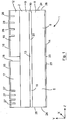
- a typical tunable laser device indicated generally by the reference numeral 1.
- the tunable laser device 1 as will be described below is tunable for producing laser light of selectable wavelengths within a relatively wide range of wavelengths about a centre wavelength, and the tuning may be continuous over the range of wavelengths or discontinuous.
- tuning is continuous the wavelength of the light produced by the laser device 1 is progressively variable over the wavelength range from the lowest wavelength of the range to the highest wavelength of the range or vice-versa.
- tuning is discontinuous the wavelength of the light is variable in steps, which may not necessarily progress sequentially from the lowest wavelength of the range to the highest thereof or vice versa.
- the tunable laser device 1 is formed as a single integral waveguide unit by an integral ridge waveguide 2 which forms a first ridge waveguide 5 and a second ridge waveguide 6 arranged in series with each other, which co-operate as will be described below for producing light of the selectable wavelengths using a Vernier-tuning principle.
- an integral ridge waveguide 2 which forms a first ridge waveguide 5 and a second ridge waveguide 6 arranged in series with each other, which co-operate as will be described below for producing light of the selectable wavelengths using a Vernier-tuning principle.
- the construction of the first and second waveguides 5 and 6 in the integral ridge waveguide 2 will first be described.
- the integral ridge waveguide 2 comprises a lower cladding layer 8 and an upper cladding layer 9, between which is located an active layer 10, which in this embodiment of the invention is formed by a plurality of quantum well layers.
- a ridge 12 formed in the upper cladding layer extends upwardly from the upper cladding layer 9, and defines a longitudinally extending light guiding region 13.
- the ridge 12 defines the lateral width in the X-direction of the light guiding region 13 in the active layer 10.
- the light guiding region 13 extends into adjacent portions of the lower and upper cladding layers 8 and 9 adjacent the active layer 10 beneath the ridge 12.
- a lower electrically conductive layer 14 on the underside of the lower cladding layer 8 and an upper electrically conductive layer 15 on the ridge 12 are provided for facilitating pumping of the first and second waveguides 5 and 6 with respective pumping currents as will be described below.
- the upper and lower cladding layers 8 and 9, the active region 10 and the ridge 12 form corresponding upper and lower cladding layers, active layers and ridges of the first and second waveguides 5 and 6.
- An electrical isolating means comprising an electrical isolating slot 16 extends into and laterally across the ridge 12 to define the first and second waveguides 5 and 6 in the integral ridge waveguide 2, and also for electrically isolating the first and second waveguides 5 and 6 for permitting pumping of the first and second waveguides 5 and 6 with respective electrical pumping currents independently of each other.
- the isolating slot 16 also forms the ridge 12 into first and second ridges 17 and 18, respectively, of the first and second waveguides 5 and 6.
- the isolating slot 16 also defines first and second light guiding regions 19 and 20, respectively, of the respective first and second waveguides 5 and 6 in the light guiding region 13 of the integral ridge waveguide 2.
- First and second proximal ends 22 and 23 of the first and second waveguides 5 and 6 through which light passes between the first and second light guiding regions 19 and 20 are effectively defined by the isolating slot 16.
- End facets 24 of the integral ridge waveguide 2 are cleaved to form reflective first and second distal ends 25 and 26, respectively, of the respective first and second waveguides 5 and 6.
- light of the selected wavelength is emitted through the first distal end 25 of the first waveguide 5.
- the isolating slot 16 is formed in the ridge 12 to a depth substantially similar to the depth of the ridge 12.
- a plurality of first refractive index altering means in this embodiment of the invention provided by a plurality of equi-spaced apart, centre to centre, first slots 27 are formed in and extend laterally across the first ridge 17 of the first waveguide 5 for producing respective refractive index perturbations in the first light guiding region 19 at locations corresponding to the locations of the respective first slots 27.
- the refractive index perturbations resulting from the first slots 27 cause some of the lasing modes to undergo reflections which produces a first mirror loss spectrum of the first waveguide 5 with a plurality of minimum peak values at respective first wavelength values.
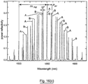
- a typical first mirror loss spectrum which will be described below, is illustrated by the waveform A of Fig. 16(a) .
- a plurality of second refractive index altering means provided by a plurality of equi-spaced apart, centre to centre, second slots 28 formed in and extending laterally across the second ridge 18 of the second waveguide 6 produce respective refractive index perturbations in the second light guiding region 20 at locations corresponding to the locations of the respective second slots 28.
- the refractive index perturbations in the second light guiding region 20 cause some of the lasing modes to undergo reflections, which produces a second mirror loss spectrum of the second waveguide 6 with a plurality of minimum peak values at respective second wavelength values.
- a typical second mirror loss spectrum which will also be described below, is illustrated by the waveform B of Fig. 16(b) .
- first and second slots 27 and 28 may be similar or may be different.
- the actual number of first and second slots may be any suitable number, and the choice of first and second slots is described in more detail below.
- the spacings of the first and second reflecting slots 27 and 28 are different to each other for producing the first and second mirror loss spectra with the minimum peak values thereof at the respective first and second wavelength values so that only one of the minimum values of the first mirror loss spectrum occurs at the same wavelength value at which one of the minimum values of the second mirror loss spectrum occurs.
- the first and second wavelength values at which the minimum peak values of the first and second mirror loss spectra occur are similar for only one of the minimum peak values of first and second mirror loss spectra.
- the first and second waveguides 5 and 6 co-operate to produce light of the wavelength value at which the two minimum peak values at the same wavelength value occur.
- the remaining modes of the light lasing in the first and second waveguides 5 and 6 are suppressed.
- the wavelength of the light produced by the laser device 1 can be selected using the principle of Vernier-tuning.
- Fig. 16(c) illustrates a typical plot of power reflectivity against wavelength for the light produced by the respective first and second waveguides 5 and 6 based on the first and second mirror loss spectra of the waveforms A and B of Figs. 16(a) and (b) .
- the waveform A of Fig. 16(c) represents the power reflectivity of light produced by the first waveguide 5 based on the first mirror loss spectrum A of Fig. 16(a) .
- the waveform B of Fig. 16(c) represent the power reflectivity of the light produced by the second waveguide 6 based on the second mirror spectrum B of Fig. 16(b) .
- 16(c) occur correspond to the wavelengths at which the minimum peak values of the first and second mirror loss spectra A and B of Figs. 16(a) and (b) , respectively, occur. Since from Figs. 16(a) and 16(b) the only common wavelength at which minimum peak values of the first and second mirror loss spectra A and B occur is approximately 1,550nm, the only wavelength at which the peak values of the power reflectivities of the light produced by the first and second waveguides 5 and 6 coincide is approximately 1,550nm. Thus, in this particular case, light is produced by the laser device 1 of wavelength of 1,550nm. By varying the wavelengths at which the minimum peak values of the first and/or second mirror loss spectra A and B of Fig. 16(a) and (b) occur, and the wavelength at which two minimum peak values, one from each of the first and second mirror loss spectrum A and B coincide, the wavelength of the light produced by the laser device 1 is varied.
- a control circuit 29 for pumping electrical currents into the first and second waveguides 5 and 6 comprises a current source 30, which is operated under the control of a microcontroller 31 for producing a pumping current for injecting into the first and second waveguides 5 and 6.
- a refractive index varying means for independently varying the refractive indices of the first and second light guiding regions 19 and 20 of the respective first and second waveguides 5 and 6 for Vernier tuning of the laser devices 1 comprises respective first and second current sources 32 and 33 for producing first and second currents for pumping the first and second waveguides 5 and 6, respectively. The first and second currents produced by the first and second current sources 32 and 33 are independently variable.
- the effective refractive indices of the first and second light guiding regions 19 and 20 of the respective first and second waveguides 5 and 6 are varied, and thus the wavelengths at which the minimum peak values of the respective first and second mirror loss spectra occur are also varied. Accordingly, by varying the first and second currents with which the first and second waveguides 5 and 6 are pumped, the wavelength of light produced by the laser device 1 can be varied. By varying the second current while holding the first current constant, or vice versa the tuning of the tunable laser device 1 is discontinuous. In other words, the wavelength of the light produced by the laser device 1 hops from one wavelength to another wavelength in wavelength steps.
- the tuning of the laser device 1 can be made to be continuous, whereby the light produced by the laser device 1 is progressively varied from light of the minimum wavelength of the tunable range to light of the maximum wavelength of the tunable range and vice versa.
- the first slot 27 which is closest to the first distal end 25 of the first waveguide 5 is spaced apart from the first distal end 25 a distance similar to the spacing between adjacent ones of the first slots 27.
- the spacing of the second slot 28 which is closest to the second distal end 26 of the second waveguide 6 is similar to the spacing between adjacent ones of the second slots 28.
- both the first and second slots 27 and 28 are located towards the respective first and second distal ends 25 and 26 of the respective first and second waveguides 5 and 6. In order that the mirror loss spectra produced by the first and second waveguides 5 and 6 are different to each other, the spacing between the second slots 28 is greater than the spacing between the first slots 27.
- the lower cladding layer 8 is of N-type material
- the upper cladding layer 9 and the ridge 12 are integrally grown and are of P-type material.
- the active layer 10 comprises five quantum well layers and is of AlGaInAs.
- the overall length of the integral ridge waveguide 2 is 800 microns, and the isolating slot 16 is located centrally intermediate the first and second distal ends 25 and 26, thereby forming the first and second waveguides 5 and 6 each of 400 microns approximately.
- the integer number N 1 is selected to be 340, the centre wavelength ⁇ is selected to be 1,550 nanometres, the average effective refractive index n 1eff,ave of the first light guiding region 19 of the first waveguide 5 in the absence of pumping current is 3.2, and thus from equation (B1) the spacing d 1 between the first slots 27 is 41 microns.
- the integer number N 2 is selected to be 360, the centre wavelength ⁇ is already selected as 1,550 nanometres, the average effective refractive index of the second light guiding cavity 20 of the second waveguide in the absence of pumping current is also 3.2, since the first and second waveguides 5 and 6 are integrally formed by the integral ridge waveguide 2.
- the spacing d 2 between the second slots 28 is 43 microns.
- the number of first slots 27 formed in the first ridge 17 of the first waveguide 5 is nine, and the number of second slots 28 formed in the second ridge 18 of the second waveguide 6 is also nine.
- the number of first and second slots is determined based on an optimisation of the reflection required to improve the selection of the selected mode over other lasing modes on the one hand and losses resulting from the first and second slots on the other hand.
- the values of the first and second pumping currents are set so that the wavelength at which the minimum peak values of the first and second mirror loss spectra produced by the first and second waveguides 5 and 6, respectively, coincide at the desired wavelength at which the light is to be produced.
- One or both of the first and second pumping currents is varied to vary the corresponding one or both of the first and second mirror loss spectra, in order to vary the wavelength of the light produced.
- a tunable laser device could be produced with a tunable wavelength range of 1,500 nanometres to 1,600 nanometres centred around a centre wavelength of 1,550 nanometres by selecting different values of the integer numbers N 1 and N 2 .
- the tunable wavelength range may be varied. This will be well known and readily apparent to those skilled in the art.
- the control circuit 29 is operated for independently pumping the first and second waveguides 5 and 6 with first and second currents, which are independent of each other, and are independently variable.
- tuning of the laser device 1 to produce light of respective selected wavelengths is discontinuous.
- tuning of the laser device 1 to produce light of selectable wavelengths can be made to be continuous, with the wavelength of the light being progressively selected from the minimum wavelength value of the selectable range to the maximum wavelength value of the selectable range and vice versa.
- the laser device 40 is integrally formed, and comprises first and second ridge waveguides 41 and 42, which for convenience will hereinafter be referred to as left and right feedback sections 41 and 42, respectively.
- Left slots 43 and right slots 44 which correspond to the first and second reflecting slots 27 and 28 are formed in the ridge 47 of the left and right feedback sections 41 and 42, respectively.
- a central gain section 45 is located between the left and right feedback sections 43 and 44 and in series therewith.
- the gain section 45 is an active section, and the left and right feedback sections 41 and 42 may be passive or active.
- the gain section 45 and the left and right feedback sections 41 and 42 are all active sections, all three sections are independently pumped and the feedback sections 41 and 42 are pumped with respective independently variable currents.
- One or both of the pumping currents which pump the left and right feedback sections 41 and 42 are varied for varying the refractive index or the refractive indices of one or both of the light guiding regions of the respective left and right feedback sections 41 and 42, depending on whether one or both pumping currents are varied.
- the wavelength of the light produced by the laser device 40 is varied.
- the left and right feedback sections 41 and 42 are passive sections, only the gain section is pumped, and independently variable tuning currents are injected into the left and right feedback sections 41 and 42, for the purpose of varying the refractive indices of one or both of the light guiding regions of the left and right feedback sections 41 and 42.
- the currents which are injected into the left and right feedback sections 41 and 42 are variable independently of each other, and variable independently of the pumping current of the gain section 45.
- left and right feedback sections 41 and 42 are considered to be passive lossless feedback sections.
- Each of the left and right slots 43 and 44 have a reflectivity r d and a transmitivity of t d .
- the distal end facets 46 have a reflectivity of r f . Since the laser device 40 comprises a gain amplifier section 45 and the left and right feedback sections 41 and 42, the gain and refractive index of the light guiding regions of each section can be controlled independently of each other by varying the currents to the respective sections.
- SMSR 1 + ⁇ r r r l r r r l 2 ⁇ n g g th 2 L cav h c 2 n sp P R .
- Fig. 7 the reflectance of a feedback section formed by 10 slots each spaced at 5 ⁇ m apart is illustrated.
- the defects are formed by a change in the real part of the refractive index in which case there is a ⁇ /2 phase change on reflection associated with them.
- This phase change not experienced by the facet reflectivity, can be compensated by adding an extra quarter wavelength to the spacing between the final slot and the adjacent facet in which case the reflectance shown in Fig. 8 is obtained. Either response leads to an enhanced reflectance at wavelength intervals governed by the slot spacing.
- Figs. 7 and 8 reflectance is plotted on the Y-axis and wavelengths in microns is plotted on the X-axis.
- m R is chosen to be 20 giving a 238nm difference in slot spacing between the left and right slots.
- the reflectance of the left and right feedback section is shown in Fig. 10 along with the absolute value of the product of the reflectivities.
- the resulting gain thresholds and the side mode suppression ratio (SMSR) are illustrated in Figs. 11 and 12 .
- Fig. 10 reflectance is plotted on the Y-axis and wavelength in microns is plotted on the X-axis.
- gain threshold in cm -1 is plotted on the Y-axis and wavelength in microns is plotted on the X-axis.
- side mode suppression ratio (SMSR) in dB is plotted on the Y-axis and wavelength in microns is plotted on the X-axis.
- ⁇ ⁇ ⁇ c m L ⁇ m R m L + 1 m R + 1 .
- ⁇ n n m L ⁇ m R m L + 1 m R + 1
- Example 1 a laser comprising of a central gain section coupled to two passive, lossless sections containing a distribution of reflectors has been described.
- a comb response can be obtained.
- non-identical grid periodicities By having non-identical grid periodicities, a single resonance can be obtained (within the gain bandwidth) at the resonance common to both mirrors.
- a very highly geared discrete tuning, between the resonances of the comb is possible by controlling the difference in index between the two feedback sections.
- a much lower geared, continuous tuning is achieved by varying the refractive indices of the light guiding regions of the left and right feedback sections simultaneously. Continuous tuning over a very large range is possible if the comb spacing matched the maximum continuous tuning range.
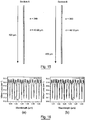
- Fig 15 illustrates two structures of a laser device according to the invention which is of a similar general construction to that of the laser device 1 described with reference to Figs. 1 to 3 .
- Fig. 16 displays the corresponding mirror loss spectra for these two feedback sections A and B with a resulting FSR of 7nm and 6.5nm.
- an electrical isolating slot which is similar to the electrical isolating slot 16 of the laser device of Figs. 1 to 3 is formed in the centre of a ridge of the structures A and B, which is similar to the ridge 12 of the laser device of Figs. 1 to 3 , so that the first and second pumping currents of the feedback sections A and B can be varied independently of each other.
- the tunable laser device is schematically illustrated in Fig. 17 , the laser device is split into two sections, namely, the first waveguide or feedback section A and the second waveguide or feedback section B by etching the isolating slot into the ridge.
- the resistance between the two sections was measured to be 1k ⁇ .
- the slot periods in the first and second feedback sections A and B are slightly different.
- the active layer consists of 5 quantum wells material InAlGaAs/InP, operating at 1310nm.
- the cavity length is 800 ⁇ m with nine slots per section the width of each slot is 1 ⁇ m with a slot depth of 0.9 ⁇ m.
- each feedback section A and B possess a slightly different periodicity, which permits the use of Vernier-effect tuning to achieve quasi-continuous wavelength coverage.
- Fig 18 illustrates another example of the calculated mirror loss spectra of the tunable laser device with the two feedback sections A and B that are similar to the ones employed in the devices of Figs. 1 to 3 and 15 to 17 .
- the number and spacing of the first and second slots in the feedback sections A and B, respectively, are selected to produce the laser device with a tuning range from 1,260 nanometres to 1,340 nanometres. Lasing occurs at the wavelength where reflection peaks of both tuning feedback sections A and B line up best, which in this case is at a wavelength of 1313 nm in the present example.
- Fig. 20 Light-current and voltage-current characteristics of the laser device are shown in Fig. 20 .
- the lasing threshold is reached at a current of 28mA and a voltage of 0.89 V.
- output power in milliwatts is plotted on one of the Y-axes, and forward voltage in volts is plotted on the other Y-axis.
- the pumping current in milliamps for the feedback sections A and B is plotted on the X-axis.
- the waveform H represents the forward voltage version of the feedback sections A and B tuning current.
- the waveform J represents the output power of the laser version of the feedback sections A and B tuning current.
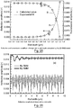
- Fig 21 shows the emission spectrum from the laser at a temperature of 25°C with the feedback sections A and B biased at 40mA respectively.
- the device lases in a single mode with an SMSR of 38.2dB.
- power in dBm is plotted on the Y-axis and wavelength in nm is plotted on the X-axis.
- the extended tuning range of the laser device was measured with a fixed current of 40mA into the feedback sections A and B with the heat sink temperature varied from 5 to 60°C.
- the discontinuous tuning jumps are due to new reflection modes coming into alignment.
- a maximum discontinuous tuning range of 30nm was achieved as shown in Fig 22 .
- wavelength in nanometres is plotted on one Y-axis and side mode suppression ratio in dB is plotted on the other Y-axis, while temperature in degrees centigrade is plotted on the X-axis.
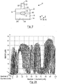
- Figs. 23 and 24 show the behaviour of the emission wavelength and the SMSR as functions of the two pumping currents of the respective feedback sections A and B.
- the heat sink temperature was fixed at 25°C.
- Fig 23 there are several bands, also referred to as super modes (which can be more easily recognised by identifying the regions of high SMSR), where continuous tuning can be carried out by varying both tuning currents simultaneously.
- super modes which can be more easily recognised by identifying the regions of high SMSR
- the emission wavelength is shifting towards longer wavelength, which is characteristic for electro thermal tuning.
- Fig. 25 a plot of reflection amplitude
- the waveform A of Fig. 25 which is a plot of reflection amplitude against slot depth
- the reflection amplitude increases with slot depth.
- the waveform B of Fig. 25 which is a plot of transmission amplitude against slot depth
- the light transmission amplitude decreases with slot depth, and thus, a trade-off must be made reflection amplitude and transmission amplitude when selecting slot depth of the first and second slots.
- the number of first and second slots it is necessary to keep the number of first and second slots to a minimum. This requires a slot pattern which provides just enough optical feedback to ensure that the laser operates in a single longitudinal mode over the wide tuning range of interest.
- the length of the first and second slots is relatively small, typically, less than 3 ⁇ m. This is required in order to ensure that the internal loss in the respective first and second light guiding regions is minimised, since the internal losses in the light guiding regions is substantially higher under the first and second slots than elsewhere in the first and second light guiding regions, and also as a result of the fact that the dopant concentration in semiconductor material at the bottom of a slot may be less than one-tenth of the level adjacent the dopant level adjacent the top of the ridge, and thus, it would be difficult if not impossible to create a low resistance metal contact on the ridge adjacent the bottom of the first and second slots.
- the length of the slots in the direction of light propagation is increased arbitrarily, a portion of the waveguide beneath the slot will remain unpumped.
- Fig. 26 illustrates a plot of reflection amplitude r against slot length in the direction of light propagation.
- the tunable laser device 70 comprises a ridge waveguide 71 which is substantially similar to the ridge waveguide 2 of the tunable laser device 1, and comprise upper and lower cladding layers 72 and 73 and an active layer 74 located between the upper and lower cladding layers 72 and 73.
- a ridge 77 formed in the upper cladding layer 72 defines a light guiding region 78 which extends the length of the waveguide 71.
- Upper and lower electrically conductive layers 80 and 81 are provided on the ridge 77 and on the lower cladding layer 73, respectively.
- the waveguide 71 defines a first waveguide 82 and a second waveguide 83, as well as a gain section 84 and a phase section 85 located intermediate the first and second waveguides 82 and 83.
- the first and second waveguides 82 and 83, the gain section 84 and the phase section 85 are arranged in series with each other.
- First and second lateral slots 86 and 87 are formed in the ridge 77 in the first waveguide 82 and the second waveguide 83 to form respective feedback sections in the first and second waveguides 82 and 83.
- An electrical isolating slot 90 electrically isolates the gain section 84 from the phase section 85, and electrical isolating slots 91 and 92 isolate the first and second waveguides 82 and 83 from the gain section 84 and the phase section 85, respectively. Accordingly, the first and second waveguides 82 and 83 and the gain and phase section 84 and 85 can be independently pumped, or electrical currents can be independently injected into the respective first and second waveguides 82 and 83 and the gain section 84 and the phase section 85, independently of each other.
- Operation of the tunable laser device 70 is substantially similar to operation of the tunable laser device 40 of Fig. 4 .
- the first and second waveguide sections 82 and 83 may be passive or active, and if active are pumped by independently variable pumping currents for varying the wavelength of light produced. If on the other hand the first and second waveguides 82 and 83 are passive, independently variable tunable currents are injected into the first and second waveguides 82 and 83 for varying the wavelength of light produced by the device 70.
- the gain region 84 is pumped independently of the first and second waveguides 82 and 83 and of the phase section 85, and a suitable phase controlling current is injected into the phase section 85 for controlling the phase of light produced by the tunable laser device 70.
- the laser devices according to the invention have been described as comprising an integral ridge waveguide which integrally incorporates the first and second ridge waveguides or feedback sections, so that the first and second light guiding regions are axially aligned and communicate directly with each other
- the tunable laser devices according to the invention may be provided by first and second waveguides separately formed, and where the first and second waveguides have been formed as two separate units, the first and second waveguides may be brought together with their respective first and second light guiding regions aligned and communicating directly with each other, or the first and second waveguides may be spaced apart from each other with the first and second light guiding regions optically coupled, and in which case, the first and second light guiding regions need not be axially aligned.
- the optical coupling of the first and second light guiding regions may be carried out by any suitable optical coupler, for example an optical fibre, a separate laser diode, or as already described, a separate gain section, or the like.
- the laser devices according to the invention may be provided by an integral ridge waveform of arcuate shape.
- the laser device according to the invention may be provided by a buried heterostructure waveguide.
- slots would be formed in the waveguide before the growth or regrowth of the upper cladding layers of such a structure.
- the laser devices according to the invention may be provided with more than two waveguides, for example, three, four or more waveguides for further enhancing the resolution between selectable wavelengths.
- Each of the ridge waveguides will include an appropriate number of refractive index altering means appropriately spaced apart in their respective ridges.
- the spacing between the refractive index altering means will be different from ridge waveguide to ridge waveguide.
- the ridge waveguides may be formed integrally in a single integral ridge waveguide, or may be formed separately of each other.
- Each ridge waveguide would be individually pumped or injected with tuning currents for facilitating independently varying the refractive indices of the light guiding regions of the respective ridge waveguides.
Landscapes
- Physics & Mathematics (AREA)
- Condensed Matter Physics & Semiconductors (AREA)
- General Physics & Mathematics (AREA)
- Electromagnetism (AREA)
- Optics & Photonics (AREA)
- Semiconductor Lasers (AREA)
Claims (15)
- Abstimmbare Laservorrichtung (1) zum Erzeugen von Licht von jeweils wählbarer Wellenlänge, wobei die abstimmbare Laservorrichtung aufweist:einen ersten Stegwellenleiter (5) aus einem Halbleitermaterial, der eine erste, sich zwischen einem ersten proximalen (22) Ende und einem ersten distalen (25) Ende erstreckende Laserdiode aufweist und einen ersten Steg (17) hat, der einen ersten lichtleitenden Bereich bildet, der sich in einer Längsrichtung zwischen seinem ersten proximalen Ende und seinem ersten distalen Ende erstreckt,einen zweiten Stegwellenleiter (6) aus einem Halbleitermaterial, der eine zweite, sich zwischen einem zweiten proximalen (23) Ende und einem zweiten distalen (26) Ende erstreckende Laserdiode aufweist und einen zweiten Steg (18) hat, der einen zweiten lichtleitenden Bereich bildet, der sich in einer Längsrichtung zwischen seinem zweiten proximalen Ende und seinem zweiten distalen Ende erstreckt,wobei die ersten und zweiten lichtleitenden Bereiche durch ihre ersten und zweiten proximalen Enden kommunizieren, und Licht der wählbaren Wellenlänge durch eines ihrer ersten und zweiten distalen Enden aussenden,eine Mehrzahl von ersten, den Brechungsindex verändernden Schlitzen (27), die im ersten Steg des ersten Wellenleiters ausgebildet sind, sich seitlich über den ersten Steg erstrecken und entlang des ersten Stegs voneinander beabstandet sind, um den Brechungsindex des ersten lichtleitenden Bereichs an voneinander beabstandeten Stellen darin zu ändern, um ein erstes Spiegelverlustspektrum mit minimalen Spitzenwerten bei jeweiligen ersten Wellenlängenwerten zu erzeugen, eine Mehrzahl von zweiten, den Brechungsindex verändernden Schlitzen (28), die im zweiten Steg des zweiten Wellenleiters ausgebildet sind, sich seitlich über den zweiten Steg erstrecken und entlang des zweiten Stegs voneinander beabstandet sind, um den Brechungsindex des zweiten lichtleitenden Bereichs an voneinander beabstandeten Stellen darin zu ändern, um ein zweites Spiegelverlustspektrum mit minimalen Spitzenwerten bei jeweiligen zweiten Wellenlängenwerten zu erzeugen, undeine den Brechungsindex verändernde Einrichtung (32, 33) zum wahlweise Verändern des Brechungsindex wenigstens des ersten lichtleitenden Bereichs um so wiederum das erste Spiegelverlustspektrum zu verändern bis einer der ersten Wellenlängenwerte ähnlich einem der zweiten Wellenlängenwerte ist, um Licht einer ausgewählten Wellenlänge der Wellenlängen zu erzeugen,
wobei
die ersten den Brechungsindex verändernden Schlitze in gleichen Abständen voneinander entlang des ersten Stegs angeordnet sind, und der eine der ersten den Brechungsindex verändernden Schlitze, der dem ersten distalen Ende des ersten Wellenleiters am nächsten gelegen ist, in einem Abstand von dem ersten distalen Ende angeordnet ist, der im Wesentlichen dem Abstand zwischen benachbarten der ersten den Brechungsindex verändernden Schlitze gleicht,
der Abstand zwischen den ersten den Brechungsindex verändernden Schlitzen durch die folgenden Gleichung bestimmt wird: d1 der Mittenabstand zwischen benachbarten der ersten den Brechungsindex verändernden Schlitze ist,N1 eine ganze Zahl von Eins aufwärts ist,λ die zentrale Wellenlänge des Bereichs von Lichtwellenlängen ist, über den die Laservorrichtung abstimmbar sein soll, undn1 eff, ave der durchschnittliche effektive Brechungsindex des ersten lichtleitenden Bereichs ist,die zweiten den Brechungsindex verändernden Schlitze in gleichen Abständen voneinander entlang des zweiten Stegs angeordnet sind, und der eine der zweiten den Brechungsindex verändernden Schlitze, der dem zweiten distalen Ende des zweiten Wellenleiters am nächsten gelegen ist, in einem Abstand von dem zweiten distalen Ende angeordnet ist, der im Wesentlichen dem Abstand zwischen benachbarten der zweiten den Brechungsindex verändernden Schlitze gleicht,der Abstand zwischen den zweiten den Brechungsindex verändernden Schlitzen sich von dem Abstand zwischen den ersten den Brechungsindex verändernden Schlitzen unterscheidet, und
der Abstand zwischen den zweiten den Brechungsindex verändernden Schlitzen durch die folgenden Gleichung bestimmt wird: d2 der Mittenabstand zwischen benachbarten der zweiten den Brechungsindex verändernden Schlitze ist,N2 eine ganze Zahl von Eins aufwärts ist,λ die zentrale Wellenlänge des Bereichs von Lichtwellenlängen ist, über den die Laservorrichtung abstimmbar sein soll, undn2 eff, ave der durchschnittliche effektive Brechungsindex des zweiten lichtleitenden Bereichs ist.
 - Abstimmbare Laservorrichtung nach Anspruch 1, dadurch gekennzeichnet, dass N2 einen Wert aufweist, der sich vom Wert von N1 unterscheidet.
- Abstimmbare Laservorrichtung nach Anspruch 1 oder 2, dadurch gekennzeichnet, dass die ersten und zweiten den Brechungsindex verändernden Schlitze dazu ausgebildet sind, den Brechungsindex der jeweiligen ersten und zweiten lichtleitenden Bereiche an Stellen zu ändern, die den jeweiligen Stellen der ersten und zweiten den Brechungsindex verändernden Schlitzen entsprechen.
- Abstimmbare Laservorrichtung nach einem der vorhergehenden Ansprüche, dadurch gekennzeichnet, dass die den Brechungsindex verändernde Einrichtung eine Einrichtung aufweist, zum wahlweisen Verändern der Brechungsindizes der jeweiligen ersten und zweiten lichtleitenden Bereiche unabhängig voneinander.
- Abstimmbare Laservorrichtung nach einem der vorhergehenden Ansprüche, dadurch gekennzeichnet, dass die den Brechungsindex verändernde Einrichtung eine erste Strominjektionseinrichtung aufweist, zum Injizieren eines ersten elektrischen Stroms in den ersten Wellenleiter, um den Brechungsindex des ersten lichtleitenden Bereichs zu ändern, und eine zweite Strominjektionseinrichtung zum Injizieren eines zweiten elektrischen Stroms in den zweiten Wellenleiter, um den Brechungsindex des zweiten lichtleitenden Bereichs zu ändern.
- Abstimmbare Laservorrichtung nach Anspruch 5, dadurch gekennzeichnet, dass die ersten Strominjektionseinrichtung eine Einrichtung zum wahlweisen Ändern des ersten Stroms aufweist, und die zweite Strominjektionseinrichtung eine Einrichtung zum wahlweisen Ändern des zweiten Stroms aufweist, wobei die ersten und zweiten Strominjektionseinrichtungen unabhängig voneinander betreibbar sind, um die Werte des ersten und zweiten Stroms unabhängig voneinander zu wählen.
- Abstimmbare Laservorrichtung nach einem der vorhergehenden Ansprüche, dadurch gekennzeichnet, dass ein Verstärkungsbereich zwischen den ersten und zweiten Wellenleitern angeordnet ist, zum Erzeugen von Licht für die ersten und zweiten Wellenleiter, wobei der Verstärkungsbereich dazu ausgebildet ist, unabhängig von den ersten und zweiten Wellenleitern mit einem Pumpstrom gepumpt zu werden.
- Abstimmbare Laservorrichtung nach Anspruch 7, dadurch gekennzeichnet, dass die ersten und zweiten Wellenleiter passive Wellenleiter sind.
- Abstimmbare Laservorrichtung nach Anspruch 7, dadurch gekennzeichnet, dass die ersten und zweiten Wellenleiter aktive Wellenleiter sind und dazu ausgebildet sind, unabhängig voneinander mit jeweiligen Pumpströmen gepumpt zu werden.
- Abstimmbare Laservorrichtung nach einem beliebigen der Ansprüche 7 bis 9, dadurch gekennzeichnet, dass sich zwischen dem Verstärkungsbereich und einem der ersten und zweiten Wellenleiter ein Phasenbereich befindet, zum Steuern der Phase des Lichts.
- Laservorrichtung nach Anspruch 10, dadurch gekennzeichnet, dass der Phasenbereich dazu ausgebildet ist, unabhängig von dem Verstärkungsbereich und den ersten und zweiten Wellenleitern, mit einem Phasensteuerstrom injiziert zu werden.
- Abstimmbare Laservorrichtung nach einem der vorhergehenden Ansprüche, dadurch gekennzeichnet, dass die ersten und zweiten lichtleitenden Bereiche der jeweiligen ersten und zweiten Wellenleiter in Längsrichtung aufeinander ausgerichtet sind, so dass durch deren erste und zweite proximale Enden eine Kommunikation stattfinden kann.
- Abstimmbare Laservorrichtung nach einem der vorhergehenden Ansprüche, dadurch gekennzeichnet, dass die ersten und zweiten Wellenleiter in einem Stück aus einem einen einzigen lichtleitenden Bereich aufweisenden Stegwellenleiter gebildet sind, und dass eine elektrische Isoliereinrichtung vorgesehen ist, um den ersten Strom in dem ersten lichtleitenden Bereich und den zweiten Strom in dem zweiten lichtleitenden Bereich im Wesentlichen voneinander zu isolieren.
- Abstimmbare Laservorrichtung nach einem der vorhergehenden Ansprüche, dadurch gekennzeichnet, dass die Wellenlänge von durch die abstimmbare Laservorrichtung erzeugtem Licht unter Verwendung eines Vernier Prinzips ausgewählt wird.
- Verfahren zum Erzeugen von Licht von jeweils wählbarer Wellenlänge, wobei das Verfahren die folgenden Schritte aufweist:Bereitstellen eines ersten Stegwellenleiters (5) aus einem Halbleitermaterial, der eine erste, sich zwischen einem ersten proximalen (22) Ende und einem ersten distalen (25) Ende erstreckende Laserdiode aufweist und einen ersten Steg (17) hat, der einen ersten lichtleitenden Bereich bildet, der sich in einer Längsrichtung zwischen seinem ersten proximalen Ende und seinem ersten distalen Ende erstreckt,Bereitstellen eines zweiten Stegwellenleiters (6) aus einem Halbleitermaterial, der eine zweite, sich zwischen einem zweiten proximalen (23) Ende und einem zweiten distalen (26) Ende erstreckende Laserdiode aufweist und einen zweiten Steg (18) hat, der einen zweiten lichtleitenden Bereich bildet, der sich in einer Längsrichtung zwischen seinem zweiten proximalen Ende und seinem zweiten distalen Ende erstreckt,Bereitstellen der ersten und zweiten lichtleitenden Bereiche, die durch ihre ersten und zweiten proximalen Enden kommunizieren und Licht der wählbaren Wellenlänge durch eines der ersten und zweiten distalen Enden aussenden,Bereitstellen einer Mehrzahl von ersten, den Brechungsindex verändernden Schlitzen (27), die im ersten Steg des ersten Wellenleiters ausgebildet sind, sich seitlich über den ersten Steg erstrecken und entlang des ersten Stegs voneinander beabstandet sind, um den Brechungsindex des ersten lichtleitenden Bereichs an voneinander beabstandeten Stellen darin zu ändern, um ein erstes Spiegelverlustspektrum mit minimalen Spitzenwerten bei jeweiligen ersten Wellenlängenwerten zu erzeugen,Bereitstellen einer Mehrzahl von zweiten, den Brechungsindex verändernden Schlitzen (28), die im zweiten Stegwellenleiter ausgebildet sind, sich seitlich über den zweiten Steg erstrecken und entlang des zweiten Stegs voneinander beabstandet sind, um den Brechungsindex des zweiten lichtleitenden Bereichs an voneinander beabstandeten Stellen darin zu ändern, um ein zweites Spiegelverlustspektrum mit minimalen Spitzenwerten bei jeweiligen zweiten Wellenlängenwerten zu erzeugen,
Bereitstellen einer den Brechungsindex verändernden Einrichtung (32, 33) zum wahlweise Verändern des Brechungsindex wenigstens des ersten lichtleitenden Bereichs, und
Verändern des ersten Spiegelverlustspektrums durch Betätigen der den Brechungsindex verändernden Einrichtung, um den Brechungsindex des ersten lichtleitenden Bereichs zu verändern bis einer der ersten Wellenlängenwerte ähnlich dem einen der zweiten Wellenlängenwerte ist, bei dem der kleinste Spitzenwert des der gewählten Wellenlänge entsprechenden zweiten Spiegelverlustspektrums auftritt,
wobei
die ersten den Brechungsindex verändernden Schlitze in gleichen Abständen voneinander entlang des ersten Stegs angeordnet sind, und der eine der ersten den Brechungsindex verändernden Schlitze, der dem ersten distalen Ende des ersten Wellenleiters am nächsten gelegen ist, in einem Abstand von dem ersten distalen Ende angeordnet ist, der im Wesentlichen dem Abstand zwischen benachbarten der ersten den Brechungsindex verändernden Schlitze gleicht,
der Abstand zwischen den ersten den Brechungsindex verändernden Schlitzen durch die folgenden Gleichung bestimmt wird: d1 der Mittenabstand zwischen benachbarten der ersten den Brechungsindex verändernden Schlitze ist,N1 eine ganze Zahl von Eins aufwärts ist,λ die zentrale Wellenlänge des Bereichs von Lichtwellenlängen ist, über den die Laservorrichtung abstimmbar sein soll, undn1 eff, ave der durchschnittliche effektive Brechungsindex des ersten lichtleitenden Bereichs ist,die zweiten den Brechungsindex verändernden Schlitze in gleichen Abständen voneinander entlang des zweiten Stegs angeordnet sind, und der eine der zweiten den Brechungsindex verändernden Schlitze, der dem zweiten distalen Ende des zweiten Wellenleiters am nächsten gelegen ist, in einem Abstand von dem zweiten distalen Ende angeordnet ist, der im Wesentlichen dem Abstand zwischen benachbarten der zweiten den Brechungsindex verändernden Schlitze gleicht,der Abstand zwischen den zweiten den Brechungsindex verändernden Schlitzen sich von dem Abstand zwischen den ersten den Brechungsindex verändernden Schlitzen unterscheidet, und
der Abstand zwischen den zweiten den Brechungsindex verändernden Schlitzen durch die folgenden Gleichung bestimmt wird: d2 der Mittenabstand zwischen benachbarten der zweiten den Brechungsindex verändernden Schlitze ist,N2 eine ganze Zahl von Eins aufwärts ist,λ die zentrale Wellenlänge des Bereichs von Lichtwellenlängen ist, über den die Laservorrichtung abstimmbar sein soll, undn2 eff, ave der durchschnittliche effektive Brechungsindex des zweiten lichtleitenden Bereichs ist.
Applications Claiming Priority (2)
| Application Number | Priority Date | Filing Date | Title |
|---|---|---|---|
| IE20060692 | 2006-09-20 | ||
| PCT/IE2007/000085 WO2008035320A1 (en) | 2006-09-20 | 2007-09-20 | Vernier tuned coupled cavity ld having a ridge with voids for langitudinal mode suppression |
Publications (3)
| Publication Number | Publication Date |
|---|---|
| EP2064785A1 EP2064785A1 (de) | 2009-06-03 |
| EP2064785B1 true EP2064785B1 (de) | 2017-05-10 |
| EP2064785B9 EP2064785B9 (de) | 2017-11-08 |
Family
ID=38792143
Family Applications (2)
| Application Number | Title | Priority Date | Filing Date |
|---|---|---|---|
| EP07805475.6A Not-in-force EP2064785B9 (de) | 2006-09-20 | 2007-09-20 | Vernierabgestimmte koppelresonator-ld mit einem stegwellenleiter mit leerstellen zur unterdrückung von longitudinalen moden |
| EP07805476A Withdrawn EP2064786A2 (de) | 2006-09-20 | 2007-09-20 | Laseranordnung, lichtsignalerzeugungsanordnung und optischer resonator und verfahren zum erzeugen von licht |
Family Applications After (1)
| Application Number | Title | Priority Date | Filing Date |
|---|---|---|---|
| EP07805476A Withdrawn EP2064786A2 (de) | 2006-09-20 | 2007-09-20 | Laseranordnung, lichtsignalerzeugungsanordnung und optischer resonator und verfahren zum erzeugen von licht |
Country Status (3)
| Country | Link |
|---|---|
| US (3) | US20100290495A1 (de) |
| EP (2) | EP2064785B9 (de) |
| WO (2) | WO2008035321A2 (de) |
Families Citing this family (10)
| Publication number | Priority date | Publication date | Assignee | Title |
|---|---|---|---|---|
| WO2014085435A1 (en) * | 2012-11-30 | 2014-06-05 | Corning Incorporated | Monolithic wide wavelength tunable mid-ir laser sources |
| CN105428997B (zh) * | 2015-12-30 | 2020-02-18 | 中国科学院半导体研究所 | 单纵模且波长可调谐的多段式fp激光器 |
| US10615575B2 (en) * | 2016-11-17 | 2020-04-07 | Nanyang Technological University | Light source and method for controlling the same |
| CN113725725B (zh) | 2017-09-28 | 2025-05-02 | 苹果公司 | 使用量子阱混合技术的激光架构 |
| KR102368946B1 (ko) * | 2017-12-15 | 2022-03-04 | 한국전자통신연구원 | 파장 가변 레이저 장치 및 이를 제조하는 방법 |
| WO2020172118A1 (en) * | 2019-02-19 | 2020-08-27 | Arizona Board Of Regents On Behalf Of The University Of Arizona | Efficient generation of spatially-restructurable high-order hg-modes in a laser cavity |
| WO2021203095A1 (en) | 2020-04-03 | 2021-10-07 | Automotive Coalition For Traffic Safety, Inc. | Widely tunable, single mode emission semiconductor laser |
| CN113109296B (zh) * | 2021-05-10 | 2022-10-28 | 南开大学 | 一种基于多腔耦合游标效应的多通道微流传感器 |
| US12204155B2 (en) | 2021-09-24 | 2025-01-21 | Apple Inc. | Chip-to-chip optical coupling for photonic integrated circuits |
| US12426139B1 (en) | 2022-06-27 | 2025-09-23 | Apple Inc. | Feedback control of a diode element |
Family Cites Families (15)
| Publication number | Priority date | Publication date | Assignee | Title |
|---|---|---|---|---|
| US5305335A (en) * | 1989-12-26 | 1994-04-19 | United Technologies Corporation | Single longitudinal mode pumped optical waveguide laser arrangement |
| JP2832920B2 (ja) * | 1992-03-06 | 1998-12-09 | 日本電信電話株式会社 | 波長掃引機能付き半導体レーザ |
| US5379318A (en) * | 1994-01-31 | 1995-01-03 | Telefonaktiebolaget L M Ericsson | Alternating grating tunable DBR laser |
| JP3237733B2 (ja) | 1994-03-30 | 2001-12-10 | 日本電信電話株式会社 | 半導体レーザ |
| US6064783A (en) * | 1994-05-25 | 2000-05-16 | Congdon; Philip A. | Integrated laser and coupled waveguide |
| GB9809583D0 (en) * | 1998-05-06 | 1998-07-01 | Marconi Gec Ltd | Optical devices |
| US6909734B2 (en) * | 1999-09-02 | 2005-06-21 | Agility Communications, Inc. | High-power, manufacturable sampled grating distributed Bragg reflector lasers |
| CN1210853C (zh) * | 1999-09-03 | 2005-07-13 | 加利福尼亚大学董事会 | 带有集成光调制器的可调谐激光源 |
| WO2001022543A1 (en) * | 1999-09-23 | 2001-03-29 | The Provost, Fellows And Scholars Of The College Of The Holy And Undivided Trinity Of Queen Elizabeth Near Dublin | An optical waveguide and a method for providing an optical waveguide |
| GB2371920A (en) * | 2001-02-02 | 2002-08-07 | Marconi Caswell Ltd | Sampled Gating Distribiuted Reflector Laser |
| GB2387481B (en) * | 2002-04-10 | 2005-08-31 | Intense Photonics Ltd | Integrated active photonic device and photodetector |
| US20050226283A1 (en) * | 2004-04-05 | 2005-10-13 | Lightip Technologies Inc. | Single-mode semiconductor laser with integrated optical waveguide filter |
| GB2416427A (en) * | 2004-06-18 | 2006-01-25 | Univ Sheffield | DFB laser |
| WO2006008724A1 (en) * | 2004-07-16 | 2006-01-26 | University College Cork - National University Of Ireland, Cork | Method for designing a semiconductor laser with intracavity reflecting features, semiconductor laser and method of fabrication thereof |
| US20060215720A1 (en) * | 2005-03-24 | 2006-09-28 | Corzine Scott W | Quantum cascade laser with grating formed by a periodic variation in doping |
-
2007
- 2007-09-20 WO PCT/IE2007/000086 patent/WO2008035321A2/en not_active Ceased
- 2007-09-20 WO PCT/IE2007/000085 patent/WO2008035320A1/en not_active Ceased
- 2007-09-20 EP EP07805475.6A patent/EP2064785B9/de not_active Not-in-force
- 2007-09-20 EP EP07805476A patent/EP2064786A2/de not_active Withdrawn
- 2007-09-20 US US12/442,337 patent/US20100290495A1/en not_active Abandoned
- 2007-09-20 US US12/442,244 patent/US8238388B2/en not_active Expired - Fee Related
-
2011
- 2011-09-16 US US13/234,256 patent/US20120114003A1/en not_active Abandoned
Also Published As
| Publication number | Publication date |
|---|---|
| EP2064785B9 (de) | 2017-11-08 |
| EP2064785A1 (de) | 2009-06-03 |
| US20100046562A1 (en) | 2010-02-25 |
| US8238388B2 (en) | 2012-08-07 |
| US20100290495A1 (en) | 2010-11-18 |
| WO2008035321A3 (en) | 2008-05-08 |
| WO2008035320A1 (en) | 2008-03-27 |
| US20120114003A1 (en) | 2012-05-10 |
| EP2064786A2 (de) | 2009-06-03 |
| WO2008035321A2 (en) | 2008-03-27 |
Similar Documents
| Publication | Publication Date | Title |
|---|---|---|
| EP2064785B9 (de) | Vernierabgestimmte koppelresonator-ld mit einem stegwellenleiter mit leerstellen zur unterdrückung von longitudinalen moden | |
| US6728279B1 (en) | Widely wavelength tunable integrated semiconductor device and method for widely tuning semiconductor devices | |
| CN103858294B (zh) | 单片集成的可调谐半导体激光器 | |
| US6438150B1 (en) | Edge-emitting semiconductor laser having asymmetric interference filters | |
| US6822982B2 (en) | Device and method for providing a tunable semiconductor laser | |
| US6590924B2 (en) | Mirror and cavity designs for sampled grating distributed bragg reflector lasers | |
| US7653093B2 (en) | Widely tunable twin guide laser structure | |
| CN107078460B (zh) | 单片集成的可调谐半导体激光器 | |
| AU2002342456A1 (en) | Surface emitting DFB laser structures and array of the same for broadband communication system | |
| US9013785B2 (en) | Tunable multi-mode laser | |
| Menezo et al. | 10-wavelength 200-GHz channel spacing emitter integrating DBR lasers with a PHASAR on InP for WDM applications | |
| EP1214763B1 (de) | Lichtwellenleiter und herstellungsverfahren | |
| EP1454393B1 (de) | Phasenverschobene oberflächenemittierende dfb laserstrukturen mit verstärkenden oder absorbierenden gittern | |
| Ishii et al. | A tunable distributed amplification DFB laser diode (TDA-DFB-LD) | |
| US20020064203A1 (en) | Strip-loaded tunable distributed feedback laser | |
| EP1094574A1 (de) | Im grossem Bereich wellenlängenabstimmbare integrierte Halbleitervorrichtung und verfahren zur wellenlängenabstimmung von Halbleitervorrichtungen | |
| KR100216959B1 (ko) | 레이저 구조 | |
| Mulcahy et al. | 60 nm widely tunable three section slot laser | |
| JP2019212888A (ja) | 光送信機および多波長光送信機 | |
| EP1058358B1 (de) | Wellenlängenabstimmbare integrierte Halbleiterlaser-Vorrichtung | |
| JP4690521B2 (ja) | 広い範囲の波長で同調可能な集積化された半導体装置及び広い範囲の波長で同調可能な半導体装置のための方法 | |
| US20050226283A1 (en) | Single-mode semiconductor laser with integrated optical waveguide filter | |
| Engelstaedter et al. | Wavelength tunable laser using an interleaved rear reflector | |
| US7715090B2 (en) | Laser source | |
| Whitbread et al. | Digital wavelength-selected DBR laser |
Legal Events
| Date | Code | Title | Description |
|---|---|---|---|
| PUAI | Public reference made under article 153(3) epc to a published international application that has entered the european phase |
Free format text: ORIGINAL CODE: 0009012 |
|
| 17P | Request for examination filed |
Effective date: 20090327 |
|
| AK | Designated contracting states |
Kind code of ref document: A1 Designated state(s): AT BE BG CH CY CZ DE DK EE ES FI FR GB GR HU IE IS IT LI LT LU LV MC MT NL PL PT RO SE SI SK TR |
|
| AX | Request for extension of the european patent |
Extension state: AL BA HR MK RS |
|
| 17Q | First examination report despatched |
Effective date: 20090708 |
|
| DAX | Request for extension of the european patent (deleted) | ||
| RAP1 | Party data changed (applicant data changed or rights of an application transferred) |
Owner name: UNIVERSITY COLLEGE CORK-NATIONAL UNIVERSITY OF IRE Owner name: THE PROVOST, FELLOWS, FOUNDATION SCHOLARS, & THE O |
|
| REG | Reference to a national code |
Ref country code: DE Ref legal event code: R079 Ref document number: 602007050959 Country of ref document: DE Free format text: PREVIOUS MAIN CLASS: H01S0005062500 Ipc: H01S0005026000 |
|
| GRAP | Despatch of communication of intention to grant a patent |
Free format text: ORIGINAL CODE: EPIDOSNIGR1 |
|
| RIC1 | Information provided on ipc code assigned before grant |
Ipc: H01S 5/026 20060101AFI20160912BHEP Ipc: H01S 5/125 20060101ALN20160912BHEP Ipc: H01S 5/10 20060101ALI20160912BHEP Ipc: H01S 5/0625 20060101ALI20160912BHEP Ipc: H01S 5/12 20060101ALN20160912BHEP Ipc: H01S 5/065 20060101ALN20160912BHEP |
|
| INTG | Intention to grant announced |
Effective date: 20160927 |
|
| RIC1 | Information provided on ipc code assigned before grant |
Ipc: H01S 5/125 20060101ALN20160919BHEP Ipc: H01S 5/0625 20060101ALI20160919BHEP Ipc: H01S 5/026 20060101AFI20160919BHEP Ipc: H01S 5/12 20060101ALN20160919BHEP Ipc: H01S 5/10 20060101ALI20160919BHEP Ipc: H01S 5/065 20060101ALN20160919BHEP |
|
| RIN1 | Information on inventor provided before grant (corrected) |
Inventor name: PHELAN, RICHARD Inventor name: DONEGAN, JOHN, F. Inventor name: LU, QIAO-YIN Inventor name: GUO, WEI-HUA Inventor name: CORBETT, BRIAN Inventor name: ROYCROFT, BRENDAN, JOHN Inventor name: LAMBKIN, PAUL, MARTIN |
|
| GRAS | Grant fee paid |
Free format text: ORIGINAL CODE: EPIDOSNIGR3 |
|
| GRAA | (expected) grant |
Free format text: ORIGINAL CODE: 0009210 |
|
| AK | Designated contracting states |
Kind code of ref document: B1 Designated state(s): AT BE BG CH CY CZ DE DK EE ES FI FR GB GR HU IE IS IT LI LT LU LV MC MT NL PL PT RO SE SI SK TR |
|
| REG | Reference to a national code |
Ref country code: GB Ref legal event code: FG4D |
|
| REG | Reference to a national code |
Ref country code: AT Ref legal event code: REF Ref document number: 893237 Country of ref document: AT Kind code of ref document: T Effective date: 20170515 Ref country code: CH Ref legal event code: EP |
|
| REG | Reference to a national code |
Ref country code: IE Ref legal event code: FG4D |
|
| REG | Reference to a national code |
Ref country code: DE Ref legal event code: R096 Ref document number: 602007050959 Country of ref document: DE |
|
| REG | Reference to a national code |
Ref country code: NL Ref legal event code: MP Effective date: 20170510 |
|
| REG | Reference to a national code |
Ref country code: LT Ref legal event code: MG4D |
|
| REG | Reference to a national code |
Ref country code: AT Ref legal event code: MK05 Ref document number: 893237 Country of ref document: AT Kind code of ref document: T Effective date: 20170510 |
|
| PG25 | Lapsed in a contracting state [announced via postgrant information from national office to epo] |
Ref country code: ES Free format text: LAPSE BECAUSE OF FAILURE TO SUBMIT A TRANSLATION OF THE DESCRIPTION OR TO PAY THE FEE WITHIN THE PRESCRIBED TIME-LIMIT Effective date: 20170510 Ref country code: AT Free format text: LAPSE BECAUSE OF FAILURE TO SUBMIT A TRANSLATION OF THE DESCRIPTION OR TO PAY THE FEE WITHIN THE PRESCRIBED TIME-LIMIT Effective date: 20170510 Ref country code: LT Free format text: LAPSE BECAUSE OF FAILURE TO SUBMIT A TRANSLATION OF THE DESCRIPTION OR TO PAY THE FEE WITHIN THE PRESCRIBED TIME-LIMIT Effective date: 20170510 Ref country code: FI Free format text: LAPSE BECAUSE OF FAILURE TO SUBMIT A TRANSLATION OF THE DESCRIPTION OR TO PAY THE FEE WITHIN THE PRESCRIBED TIME-LIMIT Effective date: 20170510 Ref country code: GR Free format text: LAPSE BECAUSE OF FAILURE TO SUBMIT A TRANSLATION OF THE DESCRIPTION OR TO PAY THE FEE WITHIN THE PRESCRIBED TIME-LIMIT Effective date: 20170811 |
|
| PGFP | Annual fee paid to national office [announced via postgrant information from national office to epo] |
Ref country code: DE Payment date: 20170829 Year of fee payment: 11 |
|
| PG25 | Lapsed in a contracting state [announced via postgrant information from national office to epo] |
Ref country code: BG Free format text: LAPSE BECAUSE OF FAILURE TO SUBMIT A TRANSLATION OF THE DESCRIPTION OR TO PAY THE FEE WITHIN THE PRESCRIBED TIME-LIMIT Effective date: 20170810 Ref country code: PL Free format text: LAPSE BECAUSE OF FAILURE TO SUBMIT A TRANSLATION OF THE DESCRIPTION OR TO PAY THE FEE WITHIN THE PRESCRIBED TIME-LIMIT Effective date: 20170510 Ref country code: SE Free format text: LAPSE BECAUSE OF FAILURE TO SUBMIT A TRANSLATION OF THE DESCRIPTION OR TO PAY THE FEE WITHIN THE PRESCRIBED TIME-LIMIT Effective date: 20170510 Ref country code: IS Free format text: LAPSE BECAUSE OF FAILURE TO SUBMIT A TRANSLATION OF THE DESCRIPTION OR TO PAY THE FEE WITHIN THE PRESCRIBED TIME-LIMIT Effective date: 20170910 Ref country code: NL Free format text: LAPSE BECAUSE OF FAILURE TO SUBMIT A TRANSLATION OF THE DESCRIPTION OR TO PAY THE FEE WITHIN THE PRESCRIBED TIME-LIMIT Effective date: 20170510 Ref country code: LV Free format text: LAPSE BECAUSE OF FAILURE TO SUBMIT A TRANSLATION OF THE DESCRIPTION OR TO PAY THE FEE WITHIN THE PRESCRIBED TIME-LIMIT Effective date: 20170510 |
|
| PG25 | Lapsed in a contracting state [announced via postgrant information from national office to epo] |
Ref country code: CZ Free format text: LAPSE BECAUSE OF FAILURE TO SUBMIT A TRANSLATION OF THE DESCRIPTION OR TO PAY THE FEE WITHIN THE PRESCRIBED TIME-LIMIT Effective date: 20170510 Ref country code: RO Free format text: LAPSE BECAUSE OF FAILURE TO SUBMIT A TRANSLATION OF THE DESCRIPTION OR TO PAY THE FEE WITHIN THE PRESCRIBED TIME-LIMIT Effective date: 20170510 Ref country code: SK Free format text: LAPSE BECAUSE OF FAILURE TO SUBMIT A TRANSLATION OF THE DESCRIPTION OR TO PAY THE FEE WITHIN THE PRESCRIBED TIME-LIMIT Effective date: 20170510 Ref country code: DK Free format text: LAPSE BECAUSE OF FAILURE TO SUBMIT A TRANSLATION OF THE DESCRIPTION OR TO PAY THE FEE WITHIN THE PRESCRIBED TIME-LIMIT Effective date: 20170510 Ref country code: EE Free format text: LAPSE BECAUSE OF FAILURE TO SUBMIT A TRANSLATION OF THE DESCRIPTION OR TO PAY THE FEE WITHIN THE PRESCRIBED TIME-LIMIT Effective date: 20170510 |
|
| REG | Reference to a national code |
Ref country code: DE Ref legal event code: R097 Ref document number: 602007050959 Country of ref document: DE |
|
| PG25 | Lapsed in a contracting state [announced via postgrant information from national office to epo] |
Ref country code: IT Free format text: LAPSE BECAUSE OF FAILURE TO SUBMIT A TRANSLATION OF THE DESCRIPTION OR TO PAY THE FEE WITHIN THE PRESCRIBED TIME-LIMIT Effective date: 20170510 |
|
| PLBE | No opposition filed within time limit |
Free format text: ORIGINAL CODE: 0009261 |
|
| STAA | Information on the status of an ep patent application or granted ep patent |
Free format text: STATUS: NO OPPOSITION FILED WITHIN TIME LIMIT |
|
| 26N | No opposition filed |
Effective date: 20180213 |
|
| REG | Reference to a national code |
Ref country code: CH Ref legal event code: PL |
|
| GBPC | Gb: european patent ceased through non-payment of renewal fee |
Effective date: 20170920 |
|
| PG25 | Lapsed in a contracting state [announced via postgrant information from national office to epo] |
Ref country code: SI Free format text: LAPSE BECAUSE OF FAILURE TO SUBMIT A TRANSLATION OF THE DESCRIPTION OR TO PAY THE FEE WITHIN THE PRESCRIBED TIME-LIMIT Effective date: 20170510 Ref country code: MC Free format text: LAPSE BECAUSE OF FAILURE TO SUBMIT A TRANSLATION OF THE DESCRIPTION OR TO PAY THE FEE WITHIN THE PRESCRIBED TIME-LIMIT Effective date: 20170510 |
|
| REG | Reference to a national code |
Ref country code: IE Ref legal event code: MM4A |
|
| REG | Reference to a national code |
Ref country code: BE Ref legal event code: MM Effective date: 20170930 |
|
| PG25 | Lapsed in a contracting state [announced via postgrant information from national office to epo] |
Ref country code: LU Free format text: LAPSE BECAUSE OF NON-PAYMENT OF DUE FEES Effective date: 20170920 |
|
| REG | Reference to a national code |
Ref country code: FR Ref legal event code: ST Effective date: 20180531 |
|
| PG25 | Lapsed in a contracting state [announced via postgrant information from national office to epo] |
Ref country code: LI Free format text: LAPSE BECAUSE OF NON-PAYMENT OF DUE FEES Effective date: 20170930 Ref country code: IE Free format text: LAPSE BECAUSE OF NON-PAYMENT OF DUE FEES Effective date: 20170920 Ref country code: GB Free format text: LAPSE BECAUSE OF NON-PAYMENT OF DUE FEES Effective date: 20170920 Ref country code: CH Free format text: LAPSE BECAUSE OF NON-PAYMENT OF DUE FEES Effective date: 20170930 |
|
| PG25 | Lapsed in a contracting state [announced via postgrant information from national office to epo] |
Ref country code: FR Free format text: LAPSE BECAUSE OF NON-PAYMENT OF DUE FEES Effective date: 20171002 Ref country code: BE Free format text: LAPSE BECAUSE OF NON-PAYMENT OF DUE FEES Effective date: 20170930 |
|
| PG25 | Lapsed in a contracting state [announced via postgrant information from national office to epo] |
Ref country code: MT Free format text: LAPSE BECAUSE OF NON-PAYMENT OF DUE FEES Effective date: 20170920 |
|
| REG | Reference to a national code |
Ref country code: DE Ref legal event code: R119 Ref document number: 602007050959 Country of ref document: DE |
|
| PG25 | Lapsed in a contracting state [announced via postgrant information from national office to epo] |
Ref country code: HU Free format text: LAPSE BECAUSE OF FAILURE TO SUBMIT A TRANSLATION OF THE DESCRIPTION OR TO PAY THE FEE WITHIN THE PRESCRIBED TIME-LIMIT; INVALID AB INITIO Effective date: 20070920 |
|
| PG25 | Lapsed in a contracting state [announced via postgrant information from national office to epo] |
Ref country code: DE Free format text: LAPSE BECAUSE OF NON-PAYMENT OF DUE FEES Effective date: 20190402 |
|
| PG25 | Lapsed in a contracting state [announced via postgrant information from national office to epo] |
Ref country code: CY Free format text: LAPSE BECAUSE OF NON-PAYMENT OF DUE FEES Effective date: 20170510 |
|
| PG25 | Lapsed in a contracting state [announced via postgrant information from national office to epo] |
Ref country code: TR Free format text: LAPSE BECAUSE OF FAILURE TO SUBMIT A TRANSLATION OF THE DESCRIPTION OR TO PAY THE FEE WITHIN THE PRESCRIBED TIME-LIMIT Effective date: 20170510 |
|
| PG25 | Lapsed in a contracting state [announced via postgrant information from national office to epo] |
Ref country code: PT Free format text: LAPSE BECAUSE OF FAILURE TO SUBMIT A TRANSLATION OF THE DESCRIPTION OR TO PAY THE FEE WITHIN THE PRESCRIBED TIME-LIMIT Effective date: 20170510 |