EP2065737B1 - Appareil d'affichage de type réflexion et procédé pour la fabrication d'une plaque de guidage lumineuse - Google Patents
Appareil d'affichage de type réflexion et procédé pour la fabrication d'une plaque de guidage lumineuse Download PDFInfo
- Publication number
- EP2065737B1 EP2065737B1 EP08169747.6A EP08169747A EP2065737B1 EP 2065737 B1 EP2065737 B1 EP 2065737B1 EP 08169747 A EP08169747 A EP 08169747A EP 2065737 B1 EP2065737 B1 EP 2065737B1
- Authority
- EP
- European Patent Office
- Prior art keywords
- guide plate
- light guide
- cavities
- type display
- display apparatus
- Prior art date
- Legal status (The legal status is an assumption and is not a legal conclusion. Google has not performed a legal analysis and makes no representation as to the accuracy of the status listed.)
- Ceased
Links
Images



Classifications
-
- G—PHYSICS
- G02—OPTICS
- G02B—OPTICAL ELEMENTS, SYSTEMS OR APPARATUS
- G02B6/00—Light guides; Structural details of arrangements comprising light guides and other optical elements, e.g. couplings
- G02B6/0001—Light guides; Structural details of arrangements comprising light guides and other optical elements, e.g. couplings specially adapted for lighting devices or systems
- G02B6/0011—Light guides; Structural details of arrangements comprising light guides and other optical elements, e.g. couplings specially adapted for lighting devices or systems the light guides being planar or of plate-like form
- G02B6/0033—Means for improving the coupling-out of light from the light guide
- G02B6/0035—Means for improving the coupling-out of light from the light guide provided on the surface of the light guide or in the bulk of it
- G02B6/0036—2-D arrangement of prisms, protrusions, indentations or roughened surfaces
-
- G—PHYSICS
- G02—OPTICS
- G02B—OPTICAL ELEMENTS, SYSTEMS OR APPARATUS
- G02B6/00—Light guides; Structural details of arrangements comprising light guides and other optical elements, e.g. couplings
- G02B6/0001—Light guides; Structural details of arrangements comprising light guides and other optical elements, e.g. couplings specially adapted for lighting devices or systems
- G02B6/0011—Light guides; Structural details of arrangements comprising light guides and other optical elements, e.g. couplings specially adapted for lighting devices or systems the light guides being planar or of plate-like form
- G02B6/0065—Manufacturing aspects; Material aspects
-
- G—PHYSICS
- G02—OPTICS
- G02F—OPTICAL DEVICES OR ARRANGEMENTS FOR THE CONTROL OF LIGHT BY MODIFICATION OF THE OPTICAL PROPERTIES OF THE MEDIA OF THE ELEMENTS INVOLVED THEREIN; NON-LINEAR OPTICS; FREQUENCY-CHANGING OF LIGHT; OPTICAL LOGIC ELEMENTS; OPTICAL ANALOGUE/DIGITAL CONVERTERS
- G02F1/00—Devices or arrangements for the control of the intensity, colour, phase, polarisation or direction of light arriving from an independent light source, e.g. switching, gating or modulating; Non-linear optics
- G02F1/01—Devices or arrangements for the control of the intensity, colour, phase, polarisation or direction of light arriving from an independent light source, e.g. switching, gating or modulating; Non-linear optics for the control of the intensity, phase, polarisation or colour
- G02F1/13—Devices or arrangements for the control of the intensity, colour, phase, polarisation or direction of light arriving from an independent light source, e.g. switching, gating or modulating; Non-linear optics for the control of the intensity, phase, polarisation or colour based on liquid crystals, e.g. single liquid crystal display cells
- G02F1/133—Constructional arrangements; Operation of liquid crystal cells; Circuit arrangements
- G02F1/1333—Constructional arrangements; Manufacturing methods
- G02F1/1335—Structural association of cells with optical devices, e.g. polarisers or reflectors
-
- B—PERFORMING OPERATIONS; TRANSPORTING
- B41—PRINTING; LINING MACHINES; TYPEWRITERS; STAMPS
- B41J—TYPEWRITERS; SELECTIVE PRINTING MECHANISMS, i.e. MECHANISMS PRINTING OTHERWISE THAN FROM A FORME; CORRECTION OF TYPOGRAPHICAL ERRORS
- B41J3/00—Typewriters or selective printing or marking mechanisms characterised by the purpose for which they are constructed
- B41J3/407—Typewriters or selective printing or marking mechanisms characterised by the purpose for which they are constructed for marking on special material
- B41J3/4076—Typewriters or selective printing or marking mechanisms characterised by the purpose for which they are constructed for marking on special material printing on rewritable, bistable "electronic paper" by a focused electric or magnetic field
Definitions
- the present invention relates generally to a reflection type display apparatus and a method for manufacturing a light guide plate. More particularly, the invention relates to a reflection type display in the form of a thin film that can be used in an electronic paper display.
- an electronic paper display apparatus displays an image by moving black and white dyes using electric fields and is suitable for use in an information terminal due to its low power consumption.
- Such an electronic paper display apparatus is a reflection type display apparatus through which light cannot pass due to its material characteristics.
- the reflection type display apparatus cannot employ an illumination unit such as a back light unit located on the rear surface of a display to directly illuminate the display.
- the reflection type display cannot secure night visibility, and uses a front light unit (FLU) for illumination.
- FLU front light unit
- a reflection type display displays an image even without using any light source at a place where an external light source is connected thereto, and displays an image by illumination of an FLU at a place without any external light source.
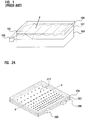
- FIG. 1 provides a perspective view that schematically illustrates an FLU structure of a conventional reflection type display apparatus.
- a conventional FLU includes a light source 103 creating and emitting light, a light guide plate 107, a light bar 101 for introducing the light emitted from the light source 103 into the light guide plate 107.
- the light guide plate 107 scatters the introduced light.
- the light guide plate 107 is provided on the upper surface of the reflection type display 109, and V-shaped grooves are formed on the upper surface of the light guide plate 107.
- the grooves having a specific angle are linearly or curvedly disposed in the longitudinal direction of the light guide plate 107 and are disposed transversely by a predetermined angle according to a predetermined rule.
- the reference numeral 105 indicates a protection film and/or a key film for protection of the light guide plate 107 or formation of keys.
- the FLU requires the light bar 101 to introduce the light into the light guide plate 107. Minute grooves (not shown) are formed in the light bar 101. The grooves of the light bar 101 change the direction of the light traveling out of the light source 103 and uniformly introduce the light through a side surface of the light guide plate 107. In other words, the light bar 101 converts a point light source to a line light source. In particular, when the light source 103 is a light emitting diode (LED), the light bar 101 is essential.
- LED light emitting diode
- the light guide plate is manufactured through injection molding or mechanical machining. More particularly, the light guide plate is made of an optically transparent material, such as plastic, through injection molding using a mold having V-shaped grooves, or is made by directly machining V-shaped grooves.
- the present invention provides a thin film shaped reflection-type display apparatus as defined by the appended independent device claim 1 and a method for manufacturing a light guide plate. as defined by the appended independent method claim 6. Further details are defined by the dependent claims.
- the present invention also provides a low-priced reflection-type display apparatus whose cavities can be rarely seen and a method for manufacturing a light guide plate.
- the present invention also provides a reflection-type display apparatus whose cavities are transversely and longitudinally disposed on the upper surface of a light guide plate and a method for manufacturing a light guide plate.
- a reflection-type display apparatus comprising: a reflection type display; a light source provided on one side of the reflection type display; a light guide plate bonded to the upper surface of the reflection type display to scatter light introduced from the light source and having cavities transversely and longitudinally disposed by predetermined intervals on the upper surface thereof; and a film bonded to the upper surface of the light guide plate to protect the upper surface of the light guide plate.
- the present invention includes a method for manufacturing a light guide plate of a reflection-type display apparatus, the method comprising: manufacturing a mask in a pattern having predetermined size and interval; lithographing cavities in a master stamper by an exposure process and a development process through use of the mask and forming cavities by an etching process; plating nickel on the master stamper and manufacturing a stamper having embossments by removing the master stamper; and forming cavities by pressing and/or heating the material of the light guide plate using the stamper.
- a thin film shaped reflection-type display apparatus is provided by manufacturing a thin film shaped flexible FLU whose cavities can not be seen. In other words, a user cannot see the cavities.
- a high-priced mold can be excluded by using a stamper to form the cavities, so as to permit a lower-priced FLU to be manufactured as compared with conventional FLUs.
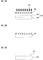
- FIGS. 2A and 2B are a perspective view and a sectional view schematically illustrating an FLU structure of a reflection type display apparatus according to an embodiment of the present invention.
- the reflection type display apparatus includes a reflection type display 209, a light source 203 provided on one side of the reflection type display 209, a light guide plate 207 bonded to the upper surface of the reflection type display 209, and a film 205 bonded to the upper surface of the light guide plate 207.
- the light source 203 and the light 207 constitute an FLU of the present invention.
- the light source 203 creates and emits light.
- the light source 203 is preferably provided on one side of the reflection type display 209.
- the light source 203 may be a light emitting diode (LED) or a cold cathode fluorescent lamp (CCFL).
- LED light emitting diode
- CCFL cold cathode fluorescent lamp
- Two light sources 203 are illustrated in the drawing, but the present invention is not limited thereto.
- the number of light sources 203 may be changed according to the size of the reflection type display 209.
- the FLU according to the exemplary embodiment of the present invention does not need a light bar that was required in the prior art due to cavities 217 of the light guide plate 207 that will be described later.
- a minimum interval is provided between the light source 203 and the light guide plate 207 to increase light introduction efficiency.
- the interval between the light source 203 and the light plate 207 is preferably below 0.2 mm.
- the light guide plate 207 scatters the light introduced from the light source 203.
- the light guide plate 207 is bonded between the upper surface of the reflection type display 209 and the lower surface of the film 205.
- the light guide plate 207 is bonded using a highly transparent adhesive or a bonding tape.
- the light guide plate 207 has a high transparency and is made of plastic such as, for example, polyvinyl chloride (PC), polyethylene terephthalate (PET), polymethylmethacrylate (PMMA), or polyurethane (PU), or silicon.
- the thickness thereof is preferably about 0.1 to 0.4 mm, and otherwise, 0.1 to 0.2 mm.
- the flexible light guide plate refers to a light guide plate whose reflection type display apparatus is used as a keypad that can be clicked. In other words, the flexible reflection type display apparatus includes keys that can be pressed by a user.
- the minimum thickness of the light guide plate 207 is preferably 0.1 mm, whereby the light guide plate guarantees the brightness of 10 nit (nit is a unit of luminance in the MKS unit system and is a brightness of a surface having a light intensity of 1 cd/m2 or 10-4 sb) that is a reference brightness commonly used in the field..
- cavities 217 are disposed by predetermined intervals on the upper surface of the light guide plate 207 that is bonded to the film 205.
- the light is guided within the light guide plate 207 by the total reflection condition.
- the guided light reaches a cavity 217, the total reflection condition is broken, whereby some light is refracted to travel out of the light guide plate 207 and some light is reflected to be guided into the light guide plate 207 until it reaches the next cavity 217.
- the light introduced into the light guide plate 207 is scattered by the cavities according to its guided distance and is used in illumination.
- FIGS. 3A and 3B are views illustrating an application of the FLU of the reflection-type display apparatus according to the exemplary embodiment of the present invention, and the functions of intervals between cavities according to the exemplary embodiment of the present invention.
- the intervals between the cavities 217 need to be regulated to obtain uniform illumination.
- the densities of the cavities 217 i.e. the numbers of cavities 217 per unit area are regulated to control distribution of brightness according to the distances between the light source 203 and the cavities 217.
- the sizes or depths of the cavities 217 may be regulated, in which case as the sizes or depths of the cavities 217 increase, the cavities 217 may be undesirably easily seen.
- the intervals between the cavities 217 is varied according to their distance from the light source 203 and the cavities have a polynomial distribution expressed in Formula 1.
- y Ax 4 + Bx 3 + Cx 2 + Dx + E
- y represents intervals between the cavities 217
- x represents distances between the light source 203 and the cavities 217
- a , B, C , D and E are properly selected according to the size and shape of the light guide plate 207.
- the intervals between the cavities 217 become larger.
- the cavities 217 are transversely and longitudinally disposed in the light guide plate 207.
- the interval functions of the cavities 217 in the light guide plate 207 are as illustrated in FIG. 3B .
- the intervals between the cavities 217 become smaller.
- the cavities 217 are curved.
- the cavities 217 have semi-spherical or conic shapes (refer to FIG. 6B ).
- the cavities 217 have diameters in this exemplary embodiment of about 30 to 50 ⁇ m and depths of about 3 to 10 ⁇ m whereby the cavities are minimally seen and the brightness of illumination is secured.
- the film 205 is provided to protect the light guide plate 207 and form a key.
- the film 205 may be a protection film or a key film, and may be formed by integrating a protection film and a key film.
- FIG. 4 is a flowchart schematically illustrating exemplary steps for manufacturing a light guide plate of the reflection-type display apparatus according to the exemplary embodiment of the present invention.
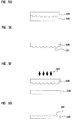
- FIGS. 5A to 5G are sectional views schematically illustrating a process of manufacturing the light guide plate of a reflection type display apparatus according to the exemplary embodiment of the present invention.
- the preferred method for manufacturing a light guide plate in a reflection type display apparatus uses a stamper.
- a mask is manufactured so as to have a pattern shape having a specific size and a specific interval (S401).
- the shape of the pattern has a specific shape to form cavities.
- the mask is manufactured such that the diameters of the cavities finally formed in the light guide plate are 30 to 50 ⁇ m and the depths thereof are 3 to 10 ⁇ m, the cavities are curved, and the intervals between cavities are defined in FIG. 1 .
- the cavities are lithographed in a master stamper by an exposure process and a development process through use of the mask (S403).
- the screens showing the performance of the processes are illustrated in FIGS. 5A and 5B .
- the mask 503 manufactured in step S401 is positioned on the master stamper 510, and light such as ultraviolet (UV) rays is projected to the mask 503 to classify the mask into necessary and unnecessary sections, whereby a photoresist (PR) 505 is hardened and an exposure process is carried out.
- the master stamper 510 includes a base 507 and a photoresist 505 located on the base 507.
- a development process in which a section of the photoresist 505 of the master stamper that has not been hardened due to failure in supply of the UV rays is removed is carried out.
- the cavities are formed in the master cylinder by an etching process (S405).
- the screen showing the performance of the process is illustrated in FIG. 5C .
- the master stamper 520 having the cavities 521 is manufactured through the etching process.
- the depths and shapes of the final cavities are determined according to etching degree.
- the cavities have spherical or conic shapes so that the surfaces of the cavities are curved.
- the cavities 217 have diameters of 30 to 50 ⁇ m and depths of 3 to 10 ⁇ m whereby the cavities are minimally seen and the brightness of illumination is secured.
- FIG. 5E The screen showing the performance of the process is illustrated in FIG. 5E .
- a stamper 530 having embossments as illustrated in FIG. 5E is manufactured by removing the master stamper 520 with the master stamper 520 being plated with nickel as in FIG. 5D .
- the picture of the embossments are illustrated in FIG. 6A.
- FIG. 6A is a picture of embossments formed in the process of manufacturing the light guide plate of the reflection type display apparatus according to the embodiment of the present invention.
- cavities are formed in the light guide plate by pressing and heating the material of the light guide plate using the stamper (S411).
- the screen showing the performance of the process is illustrated in FIGS. 5F and 5G .
- the stamper 530 having the embossments presses and heats the material 535 of the light guide plate. Then, a pressure of 5 to 6 MPa and a temperature of 180 to 200 degrees Celsius are applied.
- the light guide plate 207 may have a high transparency and may be made of plastic such as polyvinyl chloride (PC), polyethylene terephthalate (PET), polymethylmethacrylate (PMMA), or polyurethane (PU), or silicon.
- FIG. 6A is a photo of the embossments formed in the process of manufacturing the light guide plate of the reflection-type display apparatus according to the processed described hereinabove.
- the light guide plate 540 having the cavities 541 is machined so as to have a thickness of 0.1 to 0.4 mm.
- the thickness thereof is 0.1 to 0.4 mm, and otherwise, 0.1 to 0.2 mm.
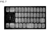
- FIG. 7 is a drawing of one type of a terminal to which the reflection-type display apparatus according to the exemplary embodiment of the present invention can be applied.
- the reflection display apparatus applied to a terminal is measured by using a luminance measurer in a dark room.
- the measurement result shows a uniformity of above 50 % and a brightness of above 10 nit and the cavities cannot be seen.
- the reflection-type display apparatus and the method for manufacturing a light guide plate according to the present invention are not limited to the above-mentioned embodiments, but may be variously modified within the scope of the appended independent claims.
Landscapes
- Physics & Mathematics (AREA)
- General Physics & Mathematics (AREA)
- Optics & Photonics (AREA)
- Engineering & Computer Science (AREA)
- Manufacturing & Machinery (AREA)
- Nonlinear Science (AREA)
- Mathematical Physics (AREA)
- Chemical & Material Sciences (AREA)
- Crystallography & Structural Chemistry (AREA)
- Planar Illumination Modules (AREA)
- Light Guides In General And Applications Therefor (AREA)
- Liquid Crystal (AREA)
Claims (7)
- Appareil d'affichage du type à réflexion comprenant:un dispositif d'affichage du type à réflexion (209);une source de lumière (203) prévue sur le dispositif d'affichage du type à réflexion (209);une plaque de guidage de lumière (207, 540) liée à la surface supérieure du dispositif d'affichage du type à réflexion (209) pour disperser la lumière introduite depuis la source de lumière (203) et à l'intérieur de laquelle sont disposées des cavités (217, 521, 541) de manière transversale et longitudinale par intervalles prédéterminés sur la surface supérieure de la plaque de guidage de lumière (207, 540);la plaque de guidage de lumière (207, 540) étant flexible; etun film (205) lié à la surface supérieure de la plaque de guidage de lumière (207, 540) pour protéger la surface supérieure de la plaque de guidage de lumière (207, 540);dans lequel les cavités (217, 521, 541) possèdent des surfaces qui sont de forme semi-sphérique ou conique;dans lequel l'épaisseur de la plaque de guidage de lumière (207, 540) se situe dans la plage allant de 0,1 à 0,2 mm.
- Appareil d'affichage du type à réflexion selon la revendication 1, dans lequel les cavités (217, 521, 541) possèdent des surfaces qui sont incurvées.
- Appareil d'affichage du type à réflexion selon les revendications 1 ou 2, dans lequel les diamètres des cavités (217, 541) se situent dans la plage allant de 30 à 50 µm et leur profondeur se situe dans la plage allant de 3 à 10 µm.
- Appareil d'affichage du type à réflexion selon l'une quelconque des revendications 1 à 3, dans lequel le film (205) comprend au moins un film parmi un film de protection, un film à touches et un film (205) dans lequel sont intégrés un film de protection et un film à touches.
- Appareil d'affichage du type à réflexion selon la revendication 1, dans lequel la source de guidage de lumière est agencée de manière adjacente à un côté du dispositif d'affichage du type à réflexion (209).
- Procédé de fabrication d'une plaque de guidage de lumière (207, 540) d'un appareil d'affichage du type à réflexion, le procédé comprenant:la fabrication (S401) d'un masque (503) selon un motif ayant des dimensions et un intervalle prédéterminés ;la lithographie (S403) de cavités (217, 521, 541) dans une matrice mère (510, 520) au moyen d'un processus d'exposition et d'un processus de développement utilisant le masque (503), et la formation (S405) des cavités (217, 521, 541) au moyen d'un processus de gravure ;le dépôt (S407) de nickel sur la matrice mère (510, 520) et la fabrication (S409) d'une matrice (530) comportant des bossages par retrait (S409) de la matrice mère (510, 520) ; etla formation des cavités (217, 521, 541) par pressage et/ou chauffage (S411) du matériau (S35) sur la plaque de guidage de lumière (207, 540) en utilisant la matrice (530) ;la liaison d'un film (205) à la surface supérieure de la plaque de guidage de lumière (207, 540) pour protéger la surface supérieure de la plaque de guidage de lumière (207, 540) ;dans lequel la plaque de guidage de lumière (207, 540) est flexible,dans lequel les cavités (217, 521, 541) possèdent des surfaces qui sont de forme semi-sphérique ou conique; et comprenant en outre, après la formation des cavités (217, 521, 541) dans la plaque de guidage de lumière (207, 540), l'usinage de la plaque de guidage de lumière (207, 540) de façon que son épaisseur se situe dans la plage allant de 0,1 à 0,2 mm.
- Procédé selon la revendication 6, dans lequel, à l'étape de formation des cavités (217, 521, 541), une pression se situant dans la plage allant de 5 à 6 MPa et une température se situant dans la plage allant de 180 à 200 degrés Celsius sont appliquées.
Applications Claiming Priority (1)
| Application Number | Priority Date | Filing Date | Title |
|---|---|---|---|
| KR1020070121905A KR101454171B1 (ko) | 2007-11-28 | 2007-11-28 | 반사형 디스플레이 장치 및 도광판의 제조 방법 |
Publications (3)
| Publication Number | Publication Date |
|---|---|
| EP2065737A2 EP2065737A2 (fr) | 2009-06-03 |
| EP2065737A3 EP2065737A3 (fr) | 2011-06-29 |
| EP2065737B1 true EP2065737B1 (fr) | 2016-03-16 |
Family
ID=40434883
Family Applications (1)
| Application Number | Title | Priority Date | Filing Date |
|---|---|---|---|
| EP08169747.6A Ceased EP2065737B1 (fr) | 2007-11-28 | 2008-11-24 | Appareil d'affichage de type réflexion et procédé pour la fabrication d'une plaque de guidage lumineuse |
Country Status (4)
| Country | Link |
|---|---|
| US (1) | US20090135469A1 (fr) |
| EP (1) | EP2065737B1 (fr) |
| KR (1) | KR101454171B1 (fr) |
| CN (1) | CN101446727A (fr) |
Families Citing this family (27)
| Publication number | Priority date | Publication date | Assignee | Title |
|---|---|---|---|---|
| US7845841B2 (en) * | 2006-08-28 | 2010-12-07 | Qualcomm Mems Technologies, Inc. | Angle sweeping holographic illuminator |
| US7855827B2 (en) | 2006-10-06 | 2010-12-21 | Qualcomm Mems Technologies, Inc. | Internal optical isolation structure for integrated front or back lighting |
| US8107155B2 (en) | 2006-10-06 | 2012-01-31 | Qualcomm Mems Technologies, Inc. | System and method for reducing visual artifacts in displays |
| US7733439B2 (en) * | 2007-04-30 | 2010-06-08 | Qualcomm Mems Technologies, Inc. | Dual film light guide for illuminating displays |
| US20090154198A1 (en) * | 2007-12-14 | 2009-06-18 | Joo Hoon Lee | Reflection type display apparatus |
| US8654061B2 (en) | 2008-02-12 | 2014-02-18 | Qualcomm Mems Technologies, Inc. | Integrated front light solution |
| WO2009102731A2 (fr) | 2008-02-12 | 2009-08-20 | Qualcomm Mems Technologies, Inc. | Dispositifs et procédés permettant d'améliore la luminosité d'écrans utilisant des couches de conversion d'angle |
| WO2009129264A1 (fr) | 2008-04-15 | 2009-10-22 | Qualcomm Mems Technologies, Inc. | Lumière ayant une propagation bidirectionnelle |
| RU2010147803A (ru) * | 2008-05-28 | 2012-07-10 | Квалкомм Мемс Текнолоджис, Инк. (Us) | Подсвечивающие устройства для фронтальной подсветки и способы их изготовления |
| US8358266B2 (en) | 2008-09-02 | 2013-01-22 | Qualcomm Mems Technologies, Inc. | Light turning device with prismatic light turning features |
| US20100051089A1 (en) * | 2008-09-02 | 2010-03-04 | Qualcomm Mems Technologies, Inc. | Light collection device with prismatic light turning features |
| CN102272516A (zh) | 2009-01-13 | 2011-12-07 | 高通Mems科技公司 | 大面积光面板及屏幕 |
| WO2010138761A1 (fr) | 2009-05-29 | 2010-12-02 | Qualcomm Mems Technologies, Inc. | Dispositifs d'éclairage et leurs procédés de fabrication |
| WO2010138762A1 (fr) * | 2009-05-29 | 2010-12-02 | Qualcomm Mems Technologies, Inc. | Dispositifs d'éclairage pour afficheurs réflexifs |
| FI20095636L (fi) * | 2009-06-08 | 2010-12-09 | Marimils Oy | Näyttöjärjestelmä ja -laite |
| US20110169428A1 (en) * | 2010-01-08 | 2011-07-14 | Qualcomm Mems Technologies, Inc. | Edge bar designs to mitigate edge shadow artifact |
| US8402647B2 (en) | 2010-08-25 | 2013-03-26 | Qualcomm Mems Technologies Inc. | Methods of manufacturing illumination systems |
| US8902484B2 (en) | 2010-12-15 | 2014-12-02 | Qualcomm Mems Technologies, Inc. | Holographic brightness enhancement film |
| WO2012122306A2 (fr) | 2011-03-08 | 2012-09-13 | Dolby Laboratories Licensing Corporation | Illuminateur pour afficheurs réflexifs |
| KR101208402B1 (ko) | 2011-10-07 | 2012-12-05 | 동우 화인켐 주식회사 | 도광판 및 이를 포함하는 백라이트 유닛 |
| KR20140020493A (ko) * | 2012-08-08 | 2014-02-19 | 삼성디스플레이 주식회사 | 도광판 및 그 제조 방법 |
| US9470834B2 (en) * | 2014-12-01 | 2016-10-18 | Shenzhen China Star Optoelectronics Technology Co., Ltd | Light guide plate and manufacturing method thereof |
| CN104503016B (zh) * | 2014-12-01 | 2018-01-02 | 深圳市华星光电技术有限公司 | 导光板及其制作方法 |
| JP6457872B2 (ja) | 2015-04-10 | 2019-01-23 | 株式会社ジャパンディスプレイ | 表示装置、照明装置、導光板及びその製造方法 |
| KR20180016407A (ko) * | 2015-05-15 | 2018-02-14 | 코닝 인코포레이티드 | 광 추출 피쳐들을 포함하는 유리 제품 및 그 제조 방법 |
| US10302847B2 (en) | 2015-05-22 | 2019-05-28 | Microsoft Technology Licensing, Llc | Micro injection-molded articles |
| KR20190117039A (ko) | 2018-04-05 | 2019-10-16 | 삼성디스플레이 주식회사 | 표시 장치, 광학 부재 및 광학 부재 제조 방법 |
Citations (1)
| Publication number | Priority date | Publication date | Assignee | Title |
|---|---|---|---|---|
| EP0878720A1 (fr) * | 1996-09-24 | 1998-11-18 | Seiko Epson Corporation | Illuminant et panneau afficheur l'utilisant |
Family Cites Families (14)
| Publication number | Priority date | Publication date | Assignee | Title |
|---|---|---|---|---|
| TW377401B (en) * | 1995-06-16 | 1999-12-21 | Kuraray Co | Method of manufacturing light guide member |
| US6224223B1 (en) * | 1997-12-22 | 2001-05-01 | Casio Computer Co., Ltd. | Illumination panel and display device using the same |
| CN1272922A (zh) * | 1998-06-02 | 2000-11-08 | 日本写真印刷株式会社 | 配置前照光的触摸屏装置 |
| JP3527961B2 (ja) * | 1999-04-30 | 2004-05-17 | 株式会社日立製作所 | フロントライト型反射液晶表示装置 |
| US20010055076A1 (en) * | 2000-04-28 | 2001-12-27 | Keizou Ochi | Reflective liquid crystal display apparatus |
| JP2002214583A (ja) * | 2000-12-28 | 2002-07-31 | Nokia Mobile Phones Ltd | タッチパネル一体型反射型lcd装置および電子装置 |
| JP2003029258A (ja) * | 2001-07-19 | 2003-01-29 | Omron Corp | 反射型表示装置及び携帯情報機器 |
| JP2004177806A (ja) * | 2002-11-28 | 2004-06-24 | Alps Electric Co Ltd | 反射防止構造および照明装置と液晶表示装置並びに反射防止膜成型用金型 |
| US7537369B2 (en) * | 2003-02-28 | 2009-05-26 | Sharp Kabushiki Kaisha | Surface radiation conversion element, liquid crystal display device, and method of producing a surface radiation conversion element |
| JP2004349182A (ja) * | 2003-05-23 | 2004-12-09 | Omron Corp | フロントライト及び反射型表示装置 |
| TWI275878B (en) * | 2004-05-13 | 2007-03-11 | Nano Prec Corp | Method for manufacturing a light guiding plate and a light guiding plate with wrinkled patterns |
| CN100419522C (zh) * | 2005-08-19 | 2008-09-17 | 鸿富锦精密工业(深圳)有限公司 | 导光板和背光系统 |
| KR100824565B1 (ko) | 2006-06-23 | 2008-04-23 | 주식회사 골든오일 | 정보 처리방법 및 시스템과 이를 위한 프로그램 기록매체 |
| US7404659B2 (en) * | 2006-11-21 | 2008-07-29 | Chien-Chin MAI | Backlight module |
-
2007
- 2007-11-28 KR KR1020070121905A patent/KR101454171B1/ko not_active Expired - Fee Related
-
2008
- 2008-11-05 CN CNA200810172867XA patent/CN101446727A/zh active Pending
- 2008-11-24 EP EP08169747.6A patent/EP2065737B1/fr not_active Ceased
- 2008-11-25 US US12/313,797 patent/US20090135469A1/en not_active Abandoned
Patent Citations (1)
| Publication number | Priority date | Publication date | Assignee | Title |
|---|---|---|---|---|
| EP0878720A1 (fr) * | 1996-09-24 | 1998-11-18 | Seiko Epson Corporation | Illuminant et panneau afficheur l'utilisant |
Also Published As
| Publication number | Publication date |
|---|---|
| KR101454171B1 (ko) | 2014-10-27 |
| KR20090055137A (ko) | 2009-06-02 |
| CN101446727A (zh) | 2009-06-03 |
| EP2065737A3 (fr) | 2011-06-29 |
| US20090135469A1 (en) | 2009-05-28 |
| EP2065737A2 (fr) | 2009-06-03 |
Similar Documents
| Publication | Publication Date | Title |
|---|---|---|
| EP2065737B1 (fr) | Appareil d'affichage de type réflexion et procédé pour la fabrication d'une plaque de guidage lumineuse | |
| US6425675B2 (en) | Planar light source and display device using the same | |
| JP7386786B2 (ja) | 光学デバイス | |
| JP5707548B2 (ja) | 光ガイド | |
| US8851734B2 (en) | Light guiding film having light extraction features | |
| US7588365B2 (en) | Method of manufacturing light guide plate, light guide plate, backlight unit with the light guide plate and display apparatus having the same | |
| EP1876482B1 (fr) | Élément guide de lumière et unité de rétroéclairage incluant l'élément guide de lumière et procédés pour la fabrication d'éléments guides de lumière et d'unités de rétroéclairage | |
| JP5809629B2 (ja) | 光導波路 | |
| US20040125590A1 (en) | Light guide plate and surface light source | |
| JP3769327B2 (ja) | プリズムレンズシート、バックライトシステム及び液晶表示装置 | |
| EP0882930A1 (fr) | Source lumineuse superficielle et affichage a cristaux liquides, et equipements de signalisation et de regulation du trafic l'utilisant | |
| WO2006129418A1 (fr) | Affichage à cristaux liquides, procédé de fabrication de feuille optique et feuille optique | |
| KR20110126741A (ko) | 광 가이드들 | |
| KR20090060158A (ko) | 면 발광 장치, 도광판 및 도광판의 제조 방법 | |
| WO2005031446A1 (fr) | Panneau lumineux, plaque de guidage de la lumiere, procede de fabrication d'une plaque de diffusion et d'une plaque de guidage de la lumiere, et dispositif a cristaux liquides | |
| JP4423933B2 (ja) | 光学シートとそれを用いたバックライトユニットおよびディスプレイ | |
| US9110211B2 (en) | Light guide plate for plane light source, method for manufacturing the same, and plane light source unit using the same | |
| JP2010218693A (ja) | 点状光源用導光板 | |
| TW202004289A (zh) | 顯示裝置、背光元件及其光耦合裝置 | |
| JP2001312915A (ja) | 面光源素子およびそれを用いた表示装置 | |
| JP2005050789A (ja) | 面光源素子およびそれを用いた表示装置 | |
| KR20160047440A (ko) | 광학 시트를 구비한 도광판 및 이를 포함하는 백라이트 유닛 | |
| JP4443723B2 (ja) | 面光源素子およびそれを用いた表示装置 | |
| WO2012147741A1 (fr) | Feuille optique | |
| US20050084228A1 (en) | Planar light device |
Legal Events
| Date | Code | Title | Description |
|---|---|---|---|
| PUAI | Public reference made under article 153(3) epc to a published international application that has entered the european phase |
Free format text: ORIGINAL CODE: 0009012 |
|
| 17P | Request for examination filed |
Effective date: 20081124 |
|
| AK | Designated contracting states |
Kind code of ref document: A2 Designated state(s): AT BE BG CH CY CZ DE DK EE ES FI FR GB GR HR HU IE IS IT LI LT LU LV MC MT NL NO PL PT RO SE SI SK TR |
|
| AX | Request for extension of the european patent |
Extension state: AL BA MK RS |
|
| PUAL | Search report despatched |
Free format text: ORIGINAL CODE: 0009013 |
|
| AK | Designated contracting states |
Kind code of ref document: A3 Designated state(s): AT BE BG CH CY CZ DE DK EE ES FI FR GB GR HR HU IE IS IT LI LT LU LV MC MT NL NO PL PT RO SE SI SK TR |
|
| AX | Request for extension of the european patent |
Extension state: AL BA MK RS |
|
| AKX | Designation fees paid |
Designated state(s): DE FR GB |
|
| 17Q | First examination report despatched |
Effective date: 20120410 |
|
| RAP1 | Party data changed (applicant data changed or rights of an application transferred) |
Owner name: SAMSUNG ELECTRONICS CO., LTD. |
|
| GRAP | Despatch of communication of intention to grant a patent |
Free format text: ORIGINAL CODE: EPIDOSNIGR1 |
|
| INTG | Intention to grant announced |
Effective date: 20151012 |
|
| GRAS | Grant fee paid |
Free format text: ORIGINAL CODE: EPIDOSNIGR3 |
|
| GRAA | (expected) grant |
Free format text: ORIGINAL CODE: 0009210 |
|
| AK | Designated contracting states |
Kind code of ref document: B1 Designated state(s): DE FR GB |
|
| REG | Reference to a national code |
Ref country code: GB Ref legal event code: FG4D |
|
| REG | Reference to a national code |
Ref country code: DE Ref legal event code: R096 Ref document number: 602008042793 Country of ref document: DE |
|
| REG | Reference to a national code |
Ref country code: FR Ref legal event code: PLFP Year of fee payment: 9 |
|
| REG | Reference to a national code |
Ref country code: DE Ref legal event code: R097 Ref document number: 602008042793 Country of ref document: DE |
|
| PLBE | No opposition filed within time limit |
Free format text: ORIGINAL CODE: 0009261 |
|
| STAA | Information on the status of an ep patent application or granted ep patent |
Free format text: STATUS: NO OPPOSITION FILED WITHIN TIME LIMIT |
|
| 26N | No opposition filed |
Effective date: 20161219 |
|
| REG | Reference to a national code |
Ref country code: FR Ref legal event code: PLFP Year of fee payment: 10 |
|
| REG | Reference to a national code |
Ref country code: FR Ref legal event code: PLFP Year of fee payment: 11 |
|
| PGFP | Annual fee paid to national office [announced via postgrant information from national office to epo] |
Ref country code: DE Payment date: 20181022 Year of fee payment: 11 |
|
| PGFP | Annual fee paid to national office [announced via postgrant information from national office to epo] |
Ref country code: FR Payment date: 20181029 Year of fee payment: 11 Ref country code: GB Payment date: 20181023 Year of fee payment: 11 |
|
| REG | Reference to a national code |
Ref country code: DE Ref legal event code: R119 Ref document number: 602008042793 Country of ref document: DE |
|
| GBPC | Gb: european patent ceased through non-payment of renewal fee |
Effective date: 20191124 |
|
| PG25 | Lapsed in a contracting state [announced via postgrant information from national office to epo] |
Ref country code: DE Free format text: LAPSE BECAUSE OF NON-PAYMENT OF DUE FEES Effective date: 20200603 Ref country code: FR Free format text: LAPSE BECAUSE OF NON-PAYMENT OF DUE FEES Effective date: 20191130 Ref country code: GB Free format text: LAPSE BECAUSE OF NON-PAYMENT OF DUE FEES Effective date: 20191124 |