EP2065928A2 - Halbleiterbauelement und Herstellungsverfahren dafür - Google Patents
Halbleiterbauelement und Herstellungsverfahren dafür Download PDFInfo
- Publication number
- EP2065928A2 EP2065928A2 EP08169571A EP08169571A EP2065928A2 EP 2065928 A2 EP2065928 A2 EP 2065928A2 EP 08169571 A EP08169571 A EP 08169571A EP 08169571 A EP08169571 A EP 08169571A EP 2065928 A2 EP2065928 A2 EP 2065928A2
- Authority
- EP
- European Patent Office
- Prior art keywords
- insulation layer
- semiconductor
- semiconductor device
- substrate
- wiring pattern
- Prior art date
- Legal status (The legal status is an assumption and is not a legal conclusion. Google has not performed a legal analysis and makes no representation as to the accuracy of the status listed.)
- Withdrawn
Links
Images








Classifications
-
- H—ELECTRICITY
- H10—SEMICONDUCTOR DEVICES; ELECTRIC SOLID-STATE DEVICES NOT OTHERWISE PROVIDED FOR
- H10P—GENERIC PROCESSES OR APPARATUS FOR THE MANUFACTURE OR TREATMENT OF DEVICES COVERED BY CLASS H10
- H10P54/00—Cutting or separating of wafers, substrates or parts of devices
-
- H—ELECTRICITY
- H10—SEMICONDUCTOR DEVICES; ELECTRIC SOLID-STATE DEVICES NOT OTHERWISE PROVIDED FOR
- H10W—GENERIC PACKAGES, INTERCONNECTIONS, CONNECTORS OR OTHER CONSTRUCTIONAL DETAILS OF DEVICES COVERED BY CLASS H10
- H10W74/00—Encapsulations, e.g. protective coatings
- H10W74/10—Encapsulations, e.g. protective coatings characterised by their shape or disposition
- H10W74/111—Encapsulations, e.g. protective coatings characterised by their shape or disposition the semiconductor body being completely enclosed
- H10W74/129—Encapsulations, e.g. protective coatings characterised by their shape or disposition the semiconductor body being completely enclosed forming a chip-scale package [CSP]
-
- H—ELECTRICITY
- H10—SEMICONDUCTOR DEVICES; ELECTRIC SOLID-STATE DEVICES NOT OTHERWISE PROVIDED FOR
- H10W—GENERIC PACKAGES, INTERCONNECTIONS, CONNECTORS OR OTHER CONSTRUCTIONAL DETAILS OF DEVICES COVERED BY CLASS H10
- H10W74/00—Encapsulations, e.g. protective coatings
- H10W74/10—Encapsulations, e.g. protective coatings characterised by their shape or disposition
- H10W74/131—Encapsulations, e.g. protective coatings characterised by their shape or disposition the semiconductor body being only partially enclosed
- H10W74/147—Encapsulations, e.g. protective coatings characterised by their shape or disposition the semiconductor body being only partially enclosed the encapsulations being multilayered
-
- H—ELECTRICITY
- H10—SEMICONDUCTOR DEVICES; ELECTRIC SOLID-STATE DEVICES NOT OTHERWISE PROVIDED FOR
- H10W—GENERIC PACKAGES, INTERCONNECTIONS, CONNECTORS OR OTHER CONSTRUCTIONAL DETAILS OF DEVICES COVERED BY CLASS H10
- H10W90/00—Package configurations
- H10W90/701—Package configurations characterised by the relative positions of pads or connectors relative to package parts
-
- H—ELECTRICITY
- H10—SEMICONDUCTOR DEVICES; ELECTRIC SOLID-STATE DEVICES NOT OTHERWISE PROVIDED FOR
- H10W—GENERIC PACKAGES, INTERCONNECTIONS, CONNECTORS OR OTHER CONSTRUCTIONAL DETAILS OF DEVICES COVERED BY CLASS H10
- H10W70/00—Package substrates; Interposers; Redistribution layers [RDL]
- H10W70/60—Insulating or insulated package substrates; Interposers; Redistribution layers
-
- H—ELECTRICITY
- H10—SEMICONDUCTOR DEVICES; ELECTRIC SOLID-STATE DEVICES NOT OTHERWISE PROVIDED FOR
- H10W—GENERIC PACKAGES, INTERCONNECTIONS, CONNECTORS OR OTHER CONSTRUCTIONAL DETAILS OF DEVICES COVERED BY CLASS H10
- H10W72/00—Interconnections or connectors in packages
- H10W72/20—Bump connectors, e.g. solder bumps or copper pillars; Dummy bumps; Thermal bumps
-
- H—ELECTRICITY
- H10—SEMICONDUCTOR DEVICES; ELECTRIC SOLID-STATE DEVICES NOT OTHERWISE PROVIDED FOR
- H10W—GENERIC PACKAGES, INTERCONNECTIONS, CONNECTORS OR OTHER CONSTRUCTIONAL DETAILS OF DEVICES COVERED BY CLASS H10
- H10W72/00—Interconnections or connectors in packages
- H10W72/90—Bond pads, in general
- H10W72/921—Structures or relative sizes of bond pads
- H10W72/923—Bond pads having multiple stacked layers
-
- H—ELECTRICITY
- H10—SEMICONDUCTOR DEVICES; ELECTRIC SOLID-STATE DEVICES NOT OTHERWISE PROVIDED FOR
- H10W—GENERIC PACKAGES, INTERCONNECTIONS, CONNECTORS OR OTHER CONSTRUCTIONAL DETAILS OF DEVICES COVERED BY CLASS H10
- H10W72/00—Interconnections or connectors in packages
- H10W72/90—Bond pads, in general
- H10W72/951—Materials of bond pads
- H10W72/952—Materials of bond pads comprising metals or metalloids, e.g. PbSn, Ag or Cu
Definitions
- the present invention relates to a semiconductor device and a manufacturing method thereof. More particularly, it relates to a semiconductor device which is generally equal in size to a semiconductor chip in plan configuration, and in which the semiconductor chip is flip-chip connected to a wiring pattern, and a manufacturing method thereof.
- CSP chip size package
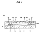
- FIG.1 is a sectional view of the conventional semiconductor device 100.
- the semiconductor device 100 includes a semiconductor chip 101, internal connection terminal 102, a resin layer 103, a wiring pattern 104, a solder resist 106 and an external connection terminal 107.
- the semiconductor chip 101 has a semiconductor substrate 109, a semiconductor integrated circuit 111, an electrode pad 112 and a protective film 113.
- the semiconductor substrate 109 is, for example, a laminated and divided Si wafer.
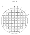
- the semiconductor integrated circuit 111 is provided on one surface of the semiconductor substrate 109 shown in Fig. 2 .
- the electrode pad 112 is provided on the semiconductor integrated circuit 111 and is electrically connected with wires provided on the semiconductor integrated circuit 111.
- the protective film 113 is provided on the semiconductor integrated circuit 111 and protects the semiconductor integrated circuit 111.
- the resin layer 103 is provided so as to cover the protective film 113 provided on the semiconductor integrated circuit 111.
- the wiring pattern 104 is formed on the resin layer 103 and has an external connection terminal provision region 104A on which the external connection terminal 107 is provided.
- the internal connection terminal 102 penetrates the resin film 103 and electrically connects the electrode pad 112 provided on the semiconductor integrated circuit 111 with the wiring pattern 104 provided on the resin layer 103.
- the solder resist 106 is provided so as to cover the wiring pattern 104 except for the external connection terminal provision region 104A.
- the external connection terminal 107 is provided on the external connection terminal provision region 104A on the wiring pattern 104.
- This semiconductor device 100 is manufactured by following steps (a) through (g).
- the semiconductor device 100 When using the semiconductor device 100 obtained by the above described method, the semiconductor device 100 is heated while using and after that, is gradually cooled. In accordance with this heating/cooling cycle, the semiconductor device 100 thermally expands or thermally contracts.
- the semiconductor chip 101 is made of silicon
- the resin layer 103 is made of resin such as polyimide resin and thermosetting epoxy resin
- the solder resist 106 is made of resin such as epoxy resin and epoxyacrylate resin
- the dimension of the semiconductor chip 101 made of silicon changes from the dimension of the resin layer 103 and the solder resist 106 which are made of resin.
- This dimensional change generates a stress which causes a peeling of the resin layer 103 from the semiconductor chip 101.
- this repetitive stress caused by using of the semiconductor device 100 invites a peeling of the resin layer 103 from the semiconductor chip 101.
- the bonding force of the resin layer 103 to the semiconductor chip 101 becomes the weakest at a corner portion and the stress due to the dimensional change becomes the strongest at the same corner portion, the peeling of the resin layer 103 starts from the corner portion of the semiconductor chip 101.
- thermosetting resin as the solder resist
- contraction is caused and the dimensional change is also generated in manufacturing the semiconductor device 100.
- the peeling of the resist film 103 can be generated even if manufacturing the semiconductor device 100.
- the present invention is achieved in view of the circumstance and an object of the present invention is to provide a semiconductor device having enhanced reliability and also to provide a manufacturing method thereof.
- a method for manufacturing a semiconductor device including:
- the method further including:
- the first insulation layer does not expose the semiconductor chips corresponding to the scribe region.
- the first insulation layer is made of a non light-sensitive insulation material.
- the second insulation layer is formed by a photolithography method including an etching processing step.
- a semiconductor device including:
- the semiconductor device further including:
- the first insulation layer is made of a non light-sensitive insulation material.
- Embodiments are also directed to apparatuses for carrying out the disclosed methods and including apparatus parts for performing described method steps. Furthermore, embodiments are also directed to methods by which the described apparatus operates or by which the described apparatus is manufactured. It may include method steps for carrying out functions of the apparatus or manufacturing parts of the apparatus. The method steps may be performed by way of hardware components, firmware, software, a computer programmed by appropriate software, by any combination thereof or in any other manner.
- Fig. 3 is a cross sectional view of a semiconductor device of a first embodiment of the invention.
- a semiconductor device 10 of the first embodiment has a semiconductor chip 11, internal connection terminals 12, an insulation layer 13 (first insulation layer), a wiring pattern 14 including a metal layer 26 and a second metal layer 27, a solder resist 16 (second insulation layer), and external connection terminals 17.
- a D part denotes a portion where a peeling off is unfavorably caused in a conventional semiconductor device. That is, a boundary between a protective layer 24 and the first insulation layer 13, which adjoins to a scribe region B explained later.
- Fig. 4 is a plan view of a semiconductor substrate on which the semiconductor devices of the first embodiment of the invention are formed.
- 31 denotes a semiconductor substrate
- C denotes a position at which the semiconductor substrate 31 is cut by a dicer (which is hereinafter referred to as a "substrate cutting position C").
- the semiconductor substrate 31 has a plurality of semiconductor device formation regions A, and a scribe region B including the substrate cutting position C, for separating a plurality of the semiconductor device formation regions A each other.
- a plurality of the semiconductor device formation regions A are the regions where the semiconductor devices 10 are formed.
- the semiconductor substrate 31 is a substrate which is laminated, and cut at the substrate cutting position C, thereby to be formed into a semiconductor substrate 21 shown in Fig. 3 .
- the semiconductor chip 11 has a semiconductor substrate 21, a semiconductor integrated circuit 22, a plurality of electrode pads 23, and a protective layer 24.
- the semiconductor substrate 21 is a substrate for forming the semiconductor integrated circuit 22.
- the semiconductor substrate 21 has been laminated.
- the thickness T 1 of the semiconductor substrate 21 can be set at, for example, 100 ⁇ m to 300 ⁇ m.
- the semiconductor substrate 21 is, for example, each individual piece obtained by cutting a laminated Si wafer.
- the semiconductor integrated circuit 22 is provided on the front surface side of the semiconductor substrate 21.
- the semiconductor integrated circuit 22 includes a diffusion layer (not shown) formed in the semiconductor substrate 21, an insulation layer (not shown) stacked on the semiconductor substrate 21, vias (not shown) provided in the stacked insulation layer, and wiring, and the like (not shown).
- a plurality of the electrode pads 23 are provided on the semiconductor integrated circuit 22.
- the electrode pads 23 are electrically connected to the wiring (not shown) provided on the semiconductor integrated circuit 22.
- the protective film 24 is provided on the semiconductor integrated circuit 22.
- the protective film 24 protects the semiconductor integrated circuit 22.
- a SiN film, a PSG (phosphor silicate glass) film, or the like can be used as the protective film 24.
- a layer including polyimide or the like is further stacked on a layer including a SiN film, a PSG film, or the like.
- Each internal connection terminal 12 is provided on each electrode pad 23.
- the internal connection terminal 12 is for electrically connecting the semiconductor integrated circuit 22 and the wiring pattern 14.
- the height H 1 of the internal connection terminal 12 can be set at, for example, 10 ⁇ m to 60 ⁇ m.
- the Au bump can be formed by, for example, a bonding process or a plating process.
- the insulation layer 13 (first insulation layer) is provided so as to cover the internal connection terminal 12 portions except for the top surfaces 12A of the internal connection terminals 12, and the semiconductor chips 11.
- the top surfaces 12A of the internal connection terminals 12 are exposed from the insulation layer 13.
- the top surface 13A of the insulation layer 13 is set generally flush with the top surfaces 12A of the internal connection terminals 12.
- a sheet-like insulation layer having adherence e.g., NCF (Non Conductive Film)
- a paste-like insulation layer e.g., NCP (Non Conductive Paste)
- the thickness T 2 of the insulation layer 13 can be set at, for example, 10 ⁇ m to 60 ⁇ m.
- the wiring pattern 14 includes the metal layer 26 and the second metal layer 27, and provided on the top surface 13A of the insulation layer 13 so as to be in contact with the top surfaces 12A of the internal connection terminals 12.
- the wiring pattern 14 is electrically connected to the semiconductor integrated circuit 22 via the internal connection terminals 12.
- the wiring pattern 14 has an external connection terminal provision region 14A in which the external connection terminals 17 are provided.
- the thickness of the wiring pattern 14 can be set at, for example, 12 ⁇ m.
- the solder resist 16 (second insulation layer) is provided so as to be opened at the external connection terminal provision region 14A and at the whole of, or a part of the scribe region B, and to cover the wiring pattern 14. Incidentally, the solder resist 16 at the portion corresponding to the substrate cutting position C is necessarily opened.
- the external connection terminals 17 are provided in the external connection terminal provision region 14A of the wiring pattern 14.
- the external connection terminals 17 are terminals to be electrically connected to the pads provided on a mounting substrate (not shown) such as a motherboard.
- solder bumps can be used as the external connection terminals 17, for example.
- the solder resist 16 is not formed on the whole of, or a part of the scribe region B of the semiconductor device 10.
- the solder resist 16 at the portion corresponding to the substrate cutting position C is necessarily opened.
- the semiconductor device 31 is cut at the substrate cutting position C, the semiconductor chips 11 and the insulation layer 13 are cut, but the solder resist 16 is not cut. Therefore, the insulation layer 13 is exposed at the outer periphery of the semiconductor device 10 (the main surface of the semiconductor chip 11 is not exposed).
- the cut plane of the insulation layer 13 and the end face of the solder resist 16 have a certain distance L 1 therebetween.
- the solder resist 16 is not formed on the whole of, or a part of the scribe region, and the solder resist 16 at the portion corresponding to the substrate cutting position C is necessarily opened. Therefore, the cut surface of the insulation layer 13 and the end face of the solder resist 16 have a certain distance L 1 therebetween, which enables the reduction of the effects of tensile stress and hardening shrinkage force exerted on the D part (releasing of the stress applied on the D part) by the solder resist 16. This can prevent the peeling off of the insulation layer from the semiconductor chips 11.
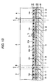
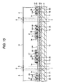
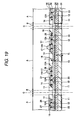
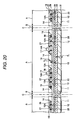
- Figs. 5 to 20 are views showing the manufacturing steps of the semiconductor device in accordance with the first embodiment of the invention.
- the same constituent parts as those of the semiconductor device 10 of the first embodiment are given the same reference numerals and signs.
- Figs. 5 to 20 the same constituent parts as those of the semiconductor device 10 of the first embodiment are given the same reference numerals and signs.
- C denotes a position at which the semiconductor substrate 31 is cut by a dicer (which is hereinafter referred to as a "substrate cutting position C") ;
- A denotes a plurality of semiconductor device formation regions (which are hereinafter referred to as “semiconductor device formation regions A”; and
- B denotes a scribe region B including the substrate cutting position C, for separating a plurality of the semiconductor device formation regions A (which is hereinafter referred to as a "scribe region B").
- the semiconductor substrate 31 having a plurality of the semiconductor device formation regions A, and a scribe region B including the substrate cutting position C, for separating a plurality of the semiconductor device formation regions A (see Fig. 4 ).
- the semiconductor substrate 31 is laminated, and cut at the substrate cutting position C, thereby to be formed into the semiconductor substrate 21 described previously (see Fig. 3 ).
- a Si wafer can be used as the semiconductor substrate 31, for example.
- the thickness T 3 of the semiconductor substrate 31 can be set at, for example, 500 ⁇ m to 775 ⁇ m.
- the semiconductor chip 11 having the semiconductor integrated circuit 22, the electrode pads 23, and the protective layer 24 is formed by a known method (semiconductor chip formation step).
- the material for the electrode pads 23, for example Al can be used.
- the internal connection terminals 12 are formed on a plurality of the electrode pads 23 provided in a plurality of the semiconductor device formation regions A, respectively (internal connection terminal formation step).
- each internal connection terminal 12 for example, there can be used an Au bump, an Au plated film, or a metal film including a Ni film formed by an electroless plating process and an Au film stacked on the Ni film.
- the Au bump can be formed by, for example, a bonding process.
- the height of a plurality of the internal connection terminals 12 formed in the step shown in Fig. 7 have deviations.
- the insulation layer 13 (first insulation layer) is formed so as to cover a plurality of the semiconductor chips 11 on the side thereof on which the internal connection terminals 12 are provided (on the front surface side of a plurality of the semiconductor chips 11) and the internal connection terminals 12 (first insulation layer formation step).
- the insulation layer 13 covers the whole surface of the semiconductor substrate including the semiconductor device formation regions A, the scribe region B and the substrate cutting position C.
- a sheet-like insulation resin having adherence property e.g., NCF (Non Conductive Film)
- a paste-like insulation resin e.g., NCP (Non Conductive Paste)
- the sheet-like insulation resin having adherence property is used, the sheet-like insulation resin is bonded on the top surface side of the structure shown in Fig. 7 to form the insulation layer 13.
- the paste-like insulation resin is used as the insulation layer 13
- the paste-like insulation resin is formed on the top surface side of the structure shown in Fig. 7 by a printing process, and then, the insulation resin is pre-baked and semi-hardened.
- the semi-hardened insulation resin has adherence property.
- the thickness T 4 of the insulation layer 13 can be set at, for example, 20 ⁇ m to 100 ⁇ m.
- a metal foil 25 is formed on the top surface 13A of the insulation layer 13. Specifically, as the metal foil 25, Cu foil is prepared and the Cu foil is bonded on the top surface 13A of the insulation layer 13.
- the thickness T 5 of the metal foil 25 can be set at, for example, 10 ⁇ m.
- the metal foil 25 is pressed from the top surface 25A side of the metal foil 25.
- the bottom surface 25B of the metal foil 25 and the top surfaces 12A of a plurality of the internal connection terminals 12 are brought in contact with each other, thereby to press bond the metal foil 25 and the internal connection terminals 12 (press bonding step).
- the insulation layer 13 is hardened.
- the thickness T 2 of the insulation layer 13 after press bonding can be set at, for example, 10 ⁇ m to 60 ⁇ m.
- the metal foil 25 is entirely removed by etching.
- the metal layer 26 is formed so as to cover the top surface of the structure shown in Fig. 11 (the top surface 13A of the insulation layer 13) by, for example, a sputtering process (metal layer formation step).
- the metal layer 26 and the internal connection terminals 12 are electrically connected.
- the metal layer 26 there can be used, for example, a Cu layer, a laminate including a Cu layer and a Cr layer, or a laminate including a Cu layer and a Ti layer.
- the metal layer 26 may be an electroless Cu-plated layer, a metal thin film layer formed by a vapor deposition process, a coating process, a chemical vapor deposition (CVD) process, or the like. Still alternatively, the foregoing metal layer formation processes may be combined.
- the thickness T 6 of the metal layer 26 can be set at, for example, 10 ⁇ m.
- the second metal layer 27 is formed so as to cover the top surface of the structure shown in Fig. 12 (the top surface 26A of the metal layer 26), for example, with the metal layer 26 as a power feed layer, by an electroplating process, or the like (metal layer formation step).
- the second metal layer 27 Cu or the like can be used as the second metal layer 27.
- the thickness T 7 of the second metal layer 27 can be set at, for example, 10 ⁇ m.
- a resist is coated on the top surface 27A of the second metal layer 27 and the resist is exposed to light, and developed, thereby to form a resist film 28 on the top surface 27A of the second metal layer 27 at the portion corresponding to the formation region of the wiring pattern 14.
- the metal layer 26 and the second metal layer 27 are etched by using the resist film 28 as a mask, thereby to remove the metal layer 26 and the second metal layer 27 at the portion on which the resist film 28 is not formed. As a result, the wiring pattern 14 is formed (wiring pattern formation step).
- the roughening processing of the wiring pattern 14 is carried out.
- the roughening processing of the wiring pattern 14 can be carried out by either process of a blackening processing or a roughening etching processing.
- the roughening processing is for improving the adhesion between the wiring pattern 14 and the solder resist 16 formed on the top surface and the side surface of the wiring pattern 14.
- a resist is coated so as to cover the tops of the wiring pattern 14 and the insulation layer 13. Then, by a photolithography process, the resist is exposed to light, and developed. The resist at the portions corresponding to the external connection terminal provision region 14A and the whole of, or a part of the scribe region B is removed by etching. As a result, the solder resist 16 (second insulation layer) having openings for exposing the external connection terminal provision region 14A and the whole of, or a part of the scribe region B is formed (second insulation layer formation step). That is, the solder resist 16 (second insulation layer) is formed on the insulation layer 13 (the first insulation layer) except for a region corresponding to the substrate cutting position C. In other words, a part of the insulation layer 13 (first insulation layer) corresponding to the substrate cutting position C of the semiconductor substrate 31 is exposed through the opening of solder resist 16 (the second insulation layer).
- the opening for exposing the whole of, or a part of the scribe region B is necessarily formed so as to expose the substrate cutting position C.
- the thickness of the solder resist 16 can be set at, for example, 25 ⁇ m.
- the width of the scribe region B can be set at, for example, 200 ⁇ m.
- the width W 1 of the opening of the solder resist 16 corresponding to the scribe region B can be set at, for example, 150 ⁇ m in view of the alignment deviation between the solder resist 16 and the structure shown in Fig. 16 , and the like.
- the semiconductor substrate 31 is polished or ground from the rear surface side of the semiconductor substrate 31, thereby to laminate the semiconductor substrate 31.
- a backside grinder can be used for lamination of the semiconductor substrate 31, for example.
- the thickness T 1 of the semiconductor substrate 31 after lamination can be set at, for example, 100 ⁇ m to 300 ⁇ m.
- the external connection terminals 17 are formed in the external connection terminal provision regions 14A of the wiring pattern 14 (external connection terminal formation step).
- the structures corresponding to the semiconductor devices 10 are formed in a plurality of the semiconductor device formation regions A.
- the semiconductor substrate 31 corresponding to the scribe region B is cut along the substrate cutting position C (cutting step) .
- cutting of the semiconductor substrate 31 is carried out by, for example, dicing.
- the solder resist 16 is not formed on the whole of, or a part of the scribe region B of the semiconductor device 10.
- the solder resist 16 at the portion corresponding to the substrate cutting position C is necessarily opened. Therefore, when the semiconductor substrate 31 is cut at the substrate cutting position C, the semiconductor chips 11 and the insulation layer 13 are cut, but the solder resist 16 is not cut. Therefore, the insulation layer 13 is exposed at the outer periphery of the semiconductor device 10 (the main surface of the semiconductor chip 11 is not exposed). A difference in level is caused at the boundary portion between the insulation film 13 and the solder resist 16.
- the solder resist 16 (second insulation layer) is not formed on the whole of, or a part of the scribe region B of the semiconductor device 10, and the solder resist 16 (second insulation layer) at the portion corresponding to the substrate cutting position C is necessarily opened.
- the cut surface of the insulation layer 13 (first insulation layer) and the end face of the solder resist 16 (second insulation layer) have a certain distance L 1 therebetween, which enables the reduction of the effects of the tensile stress and the hardening shrinkage force exerted on the D part (releasing of the stress applied on the D part) by the solder resist 16 (second insulation layer). This can prevent the peeling of the insulation layer 13 (first insulation layer) from the semiconductor chips 11, which can improve the yield of the semiconductor device 10.
- the whole semiconductor chip 11 is covered with the insulation layer 13 (first insulation layer), and the main surface of the semiconductor chip 11 is not exposed. Thus, it is possible to enhance the reliability of the semiconductor device 10.
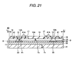
- Fig. 21 is a cross sectional view of a semiconductor device in accordance with a second embodiment of the invention.
- the same constituent parts as those of the semiconductor device 10 of the first embodiment are given the same reference numerals and signs.
- a semiconductor device 40 of the second embodiment is configured in the same manner as the semiconductor device 10, except that a wiring pattern 41 including a metal layer 26 is provided in place of the wiring pattern 14 including the metal layer 26 and the second metal layer 27 provided in the semiconductor device 10 of the first embodiment.
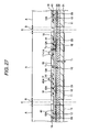
- Figs. 22 to 28 are views showing the manufacturing steps of the semiconductor device in accordance with the second embodiment of the invention.
- the same constituent parts as those of the semiconductor device 40 of the second embodiment are given the same reference numerals and signs.
- a description will be given to the manufacturing method of the semiconductor device 40 of the second embodiment.
- the metal layer 26 is etched by using the resist film 28 as a mask, thereby to remove the metal layer 26 at the portion on which the resist film 28 is not formed. As a result, the wiring pattern 41 is formed (wiring pattern formation step).
- the roughening processing of the wiring pattern 41 can be carried out by either process of a blackening processing or a roughening etching processing.
- the roughening processing is for improving the adhesion between the wiring pattern 41 and the solder resist 16 formed on the top surface and the side surface of the wiring pattern 41.
- a resist is coated so as to cover the tops of the wiring pattern 41 and the insulation layer 13. Then, by a photolithography process, the resist is exposed to light, and developed. The resist at the portions corresponding to the external connection terminal provision regions 41A and the whole of, or a part of the scribe region B is removed by etching. As a result, the solder resist 16 (second insulation layer) having openings for exposing the external connection terminal provision regions 41A and the whole of, or a part of the scribe region B is formed (second insulation layer formation step).
- the openings for exposing the whole of, or a part of the scribe region B are necessarily formed so as to expose the substrate cutting position C.
- the thickness of the solder resist 16 can be set at, for example, 25 ⁇ m.
- the width of the scribe region B can be set at, for example, 200 ⁇ m.
- the width W 1 of the opening of the solder resist 16 corresponding to the scribe region B can be set at, for example, 150 ⁇ m in view of the alignment deviation between the solder resist 16 and the structure shown in Fig. 24 , and the like.
- the semiconductor substrate 31 is polished or ground from the rear surface side of the semiconductor substrate 31, thereby to laminate the semiconductor substrate 31.
- a backside grinder can be used for lamination of the semiconductor substrate 31, for example.
- the thickness T 1 of the semiconductor substrate 31 after lamination can be set at, for example, 100 ⁇ m to 300 ⁇ m.
- the external connection terminals 17 are formed in the external connection terminal provision regions 41A of the wiring pattern 41 (external connection terminal formation step).
- the structures corresponding to the semiconductor devices 40 are formed in a plurality of the semiconductor device formation regions A.
- the semiconductor substrate 31 corresponding to the scribe region B is cut along the substrate cutting position C (cutting step) .
- cutting of the semiconductor substrate 31 is carried out by, for example, dicing.
- the solder resist 16 is not formed on the whole of, or a part of the scribe region B of the semiconductor device 40.
- the solder resist 16 at the portion corresponding to the substrate cutting position C is necessarily opened. Therefore, when the semiconductor substrate 31 is cut at the substrate cutting position C, the semiconductor chips 11 and the insulation layer 13 are cut, but the solder resist 16 is not cut. Therefore, the insulation layer 13 is exposed at the outer periphery of the semiconductor device 40 (the main surface of the semiconductor chip 11 is not exposed). Thus, the cut surface of the insulation layer 13 and the end face of the solder resist 16 have a certain distance L 1 therebetween.
- the solder resist 16 (second insulation layer) is not formed on the whole of, or a part of the scribe region B of the semiconductor device 40, and the solder resist 16 (second insulation layer) at the portion corresponding to the substrate cutting position C is necessarily opened.
- the cut surface of the insulation layer 13 (first insulation layer) and the end face of the solder resist 16 (second insulation layer) have a certain distance L 1 therebetween, which enables the reduction of the effects of the tensile stress and the hardening shrinkage force exerted on the D part (releasing of the stress applied on the D part) by the solder resist 16 (second insulation layer). This can prevent the peeling of the insulation layer 13 (the first insulation layer) from the semiconductor chips 11, which can improve the yield of the semiconductor device 40.
- the whole semiconductor chip 11 is covered with the insulation layer 13 (first insulation layer), and the main surface of the semiconductor chip 11 is not exposed, it is possible to enhance the reliability of the semiconductor device 40.
- the example in which the wiring pattern (rewiring) is formed on the first insulation layer was described.
- this invention is effective in a case where on the semiconductor chips, the first insulation layer and the second insulation layer are stacked in this order, and the second insulation layer exerts a stress on the first insulation layer, so that the semiconductor chips and the first insulation layer are peeled off from each other.
- this invention is also applicable to any semiconductor device in which rewiring is not formed so long as the semiconductor device is a semiconductor device having such a structure that the first insulation layer and the second insulation layer are stacked in this order on the semiconductor chips.
- the method for forming the wiring pattern is not limited to the methods described in the first embodiment and the second embodiment of the invention.
- the following (semi-additive) method is employed.
- a metal layer is formed on an insulation layer.
- a resist is coated on the top surface of the metal layer, and the resist is exposed to light, and developed.
- a resist film having an opening for exposing a wiring formation region is formed.
- a metal film is formed on the opening by an electroplating process, or the like, with the metal layer as a power feeding layer.
- the resist film is removed.
- the metal layer in the region in which the metal film is not formed is removed by etching.
- a wiring pattern including a metal layer and a metal film is formed.
Landscapes
- Internal Circuitry In Semiconductor Integrated Circuit Devices (AREA)
- Dicing (AREA)
- Semiconductor Integrated Circuits (AREA)
Applications Claiming Priority (1)
| Application Number | Priority Date | Filing Date | Title |
|---|---|---|---|
| JP2007300790A JP5139039B2 (ja) | 2007-11-20 | 2007-11-20 | 半導体装置及びその製造方法 |
Publications (2)
| Publication Number | Publication Date |
|---|---|
| EP2065928A2 true EP2065928A2 (de) | 2009-06-03 |
| EP2065928A3 EP2065928A3 (de) | 2011-01-26 |
Family
ID=40298658
Family Applications (1)
| Application Number | Title | Priority Date | Filing Date |
|---|---|---|---|
| EP08169571A Withdrawn EP2065928A3 (de) | 2007-11-20 | 2008-11-20 | Halbleiterbauelement und Herstellungsverfahren dafür |
Country Status (6)
| Country | Link |
|---|---|
| US (1) | US7906833B2 (de) |
| EP (1) | EP2065928A3 (de) |
| JP (1) | JP5139039B2 (de) |
| KR (1) | KR20090052282A (de) |
| CN (1) | CN101441992A (de) |
| TW (1) | TW200931595A (de) |
Families Citing this family (6)
| Publication number | Priority date | Publication date | Assignee | Title |
|---|---|---|---|---|
| JP4121542B1 (ja) * | 2007-06-18 | 2008-07-23 | 新光電気工業株式会社 | 電子装置の製造方法 |
| JP2012134270A (ja) * | 2010-12-21 | 2012-07-12 | Shinko Electric Ind Co Ltd | 半導体装置及びその製造方法 |
| US20130183823A1 (en) * | 2012-01-18 | 2013-07-18 | Chipbond Technology Corporation | Bumping process |
| JP2019054172A (ja) * | 2017-09-15 | 2019-04-04 | 東芝メモリ株式会社 | 半導体装置 |
| KR102543996B1 (ko) * | 2019-09-20 | 2023-06-16 | 주식회사 네패스 | 반도체 패키지 및 이의 제조방법 |
| CN112885793B (zh) * | 2021-03-12 | 2025-03-14 | 苏州晶方半导体科技股份有限公司 | 芯片封装结构及其制造方法 |
Family Cites Families (11)
| Publication number | Priority date | Publication date | Assignee | Title |
|---|---|---|---|---|
| JP3129161B2 (ja) | 1995-08-18 | 2001-01-29 | 松下電器産業株式会社 | チップの実装装置および実装方法 |
| US6707153B2 (en) * | 2000-03-23 | 2004-03-16 | Seiko Epson Corporation | Semiconductor chip with plural resin layers on a surface thereof and method of manufacturing same |
| JP2002057252A (ja) * | 2000-08-07 | 2002-02-22 | Hitachi Ltd | 半導体装置及びその製造方法 |
| JP5070661B2 (ja) | 2001-04-27 | 2012-11-14 | パナソニック株式会社 | 半導体装置およびその製造方法 |
| US6818475B2 (en) * | 2001-10-22 | 2004-11-16 | Wen-Kun Yang | Wafer level package and the process of the same |
| JP3614828B2 (ja) | 2002-04-05 | 2005-01-26 | 沖電気工業株式会社 | チップサイズパッケージの製造方法 |
| JP2004134709A (ja) * | 2002-10-15 | 2004-04-30 | Seiko Epson Corp | 半導体装置及びその製造方法、回路基板並びに電子機器 |
| JP2004193497A (ja) * | 2002-12-13 | 2004-07-08 | Nec Electronics Corp | チップサイズパッケージおよびその製造方法 |
| JP4322181B2 (ja) * | 2004-07-29 | 2009-08-26 | 三洋電機株式会社 | 半導体装置の製造方法 |
| JP3976043B2 (ja) * | 2004-10-25 | 2007-09-12 | セイコーエプソン株式会社 | 半導体装置及びその製造方法 |
| KR100660868B1 (ko) * | 2005-07-06 | 2006-12-26 | 삼성전자주식회사 | 칩의 배면이 몰딩된 반도체 패키지 및 그의 제조방법 |
-
2007
- 2007-11-20 JP JP2007300790A patent/JP5139039B2/ja not_active Expired - Fee Related
-
2008
- 2008-11-19 US US12/273,901 patent/US7906833B2/en active Active
- 2008-11-19 KR KR1020080114951A patent/KR20090052282A/ko not_active Withdrawn
- 2008-11-20 CN CNA2008101809569A patent/CN101441992A/zh active Pending
- 2008-11-20 EP EP08169571A patent/EP2065928A3/de not_active Withdrawn
- 2008-11-20 TW TW097144823A patent/TW200931595A/zh unknown
Also Published As
| Publication number | Publication date |
|---|---|
| US7906833B2 (en) | 2011-03-15 |
| JP5139039B2 (ja) | 2013-02-06 |
| CN101441992A (zh) | 2009-05-27 |
| KR20090052282A (ko) | 2009-05-25 |
| JP2009129982A (ja) | 2009-06-11 |
| US20090127665A1 (en) | 2009-05-21 |
| EP2065928A3 (de) | 2011-01-26 |
| TW200931595A (en) | 2009-07-16 |
Similar Documents
| Publication | Publication Date | Title |
|---|---|---|
| US8169065B2 (en) | Stackable circuit structures and methods of fabrication thereof | |
| US7968992B2 (en) | Multi-chip package structure and method of fabricating the same | |
| EP2006908B1 (de) | Elektronische Vorrichtung und dessen Herstellungsverfahren | |
| US20100078655A1 (en) | Substrate structure with die embedded inside and dual build-up layers over both side surfaces and method of the same | |
| KR20080089311A (ko) | Wlp용 다이 수용 스루홀 및 양 표면 위에 이중 사이드빌드업층들을 갖는 반도체 디바이스 패키지 및 그 방법 | |
| US7772091B2 (en) | Manufacturing method of semiconductor apparatus comprising alignment patterns in scribe regions | |
| TWI904118B (zh) | 半導體裝置以及製造半導體裝置的方法 | |
| KR102737355B1 (ko) | 반도체 디바이스 및 그의 제조 방법 | |
| US7906833B2 (en) | Semiconductor device and manufacturing method thereof | |
| WO2022052072A1 (zh) | 一种扇出型封装结构及其制备方法 | |
| JP3618330B2 (ja) | 半導体装置及びその製造方法 | |
| KR20180035113A (ko) | 전자 장치, 전자 장치의 제조 방법 및 전자 기기 | |
| EP2040294B1 (de) | Herstellungsverfahren für eine Halbleitervorrichtung | |
| US8017503B2 (en) | Manufacturing method of semiconductor package | |
| JP2004165277A (ja) | 電子部品実装構造及びその製造方法 | |
| US7964493B2 (en) | Method of manufacturing semiconductor device | |
| US7915078B2 (en) | Manufacturing method for semiconductor device embedded substrate | |
| US7763977B2 (en) | Semiconductor device and manufacturing method therefor | |
| US20100112786A1 (en) | Method of manufacturing semiconductor device | |
| US20240203803A1 (en) | Semiconductor devices and methods of manufacturing semiconductor devices | |
| WO2023079678A1 (ja) | 半導体装置およびその製造方法 | |
| US12362322B2 (en) | Method of making a fan-out semiconductor assembly with an intermediate carrier | |
| US7985619B2 (en) | Manufacturing method for semiconductor device embedded substrate | |
| KR20250160075A (ko) | 전자 장치 및 전자 장치 제조 방법 | |
| JP2000049254A (ja) | チップサイズパッケージ |
Legal Events
| Date | Code | Title | Description |
|---|---|---|---|
| PUAI | Public reference made under article 153(3) epc to a published international application that has entered the european phase |
Free format text: ORIGINAL CODE: 0009012 |
|
| AK | Designated contracting states |
Kind code of ref document: A2 Designated state(s): AT BE BG CH CY CZ DE DK EE ES FI FR GB GR HR HU IE IS IT LI LT LU LV MC MT NL NO PL PT RO SE SI SK TR |
|
| AX | Request for extension of the european patent |
Extension state: AL BA MK RS |
|
| PUAL | Search report despatched |
Free format text: ORIGINAL CODE: 0009013 |
|
| AK | Designated contracting states |
Kind code of ref document: A3 Designated state(s): AT BE BG CH CY CZ DE DK EE ES FI FR GB GR HR HU IE IS IT LI LT LU LV MC MT NL NO PL PT RO SE SI SK TR |
|
| AX | Request for extension of the european patent |
Extension state: AL BA MK RS |
|
| RIC1 | Information provided on ipc code assigned before grant |
Ipc: H01L 23/00 20060101ALN20101220BHEP Ipc: H01L 23/31 20060101ALI20101220BHEP Ipc: H01L 21/78 20060101AFI20090205BHEP |
|
| AKY | No designation fees paid | ||
| REG | Reference to a national code |
Ref country code: DE Ref legal event code: R108 |
|
| STAA | Information on the status of an ep patent application or granted ep patent |
Free format text: STATUS: THE APPLICATION IS DEEMED TO BE WITHDRAWN |
|
| REG | Reference to a national code |
Ref country code: DE Ref legal event code: R108 Effective date: 20110928 |
|
| 18D | Application deemed to be withdrawn |
Effective date: 20110607 |