EP2065965B1 - Résonateur et filtre - Google Patents
Résonateur et filtre Download PDFInfo
- Publication number
- EP2065965B1 EP2065965B1 EP08253812.5A EP08253812A EP2065965B1 EP 2065965 B1 EP2065965 B1 EP 2065965B1 EP 08253812 A EP08253812 A EP 08253812A EP 2065965 B1 EP2065965 B1 EP 2065965B1
- Authority
- EP
- European Patent Office
- Prior art keywords
- resonator
- slits
- line
- conductor line
- bent portion
- Prior art date
- Legal status (The legal status is an assumption and is not a legal conclusion. Google has not performed a legal analysis and makes no representation as to the accuracy of the status listed.)
- Ceased
Links
- 239000004020 conductor Substances 0.000 claims description 105
- 230000005540 biological transmission Effects 0.000 claims description 15
- 239000000463 material Substances 0.000 claims description 12
- 238000012986 modification Methods 0.000 description 10
- 230000004048 modification Effects 0.000 description 10
- 239000000758 substrate Substances 0.000 description 10
- 238000009826 distribution Methods 0.000 description 7
- 238000000034 method Methods 0.000 description 7
- 230000000694 effects Effects 0.000 description 4
- 230000005855 radiation Effects 0.000 description 4
- 239000006185 dispersion Substances 0.000 description 2
- 238000004519 manufacturing process Methods 0.000 description 2
- 230000002040 relaxant effect Effects 0.000 description 2
- 238000004088 simulation Methods 0.000 description 2
- 239000012141 concentrate Substances 0.000 description 1
- 230000003292 diminished effect Effects 0.000 description 1
- 230000001747 exhibiting effect Effects 0.000 description 1
- 238000009413 insulation Methods 0.000 description 1
- 238000003754 machining Methods 0.000 description 1
- 230000002265 prevention Effects 0.000 description 1
- 229910052594 sapphire Inorganic materials 0.000 description 1
- 239000010980 sapphire Substances 0.000 description 1
- 230000003245 working effect Effects 0.000 description 1
- 229910021521 yttrium barium copper oxide Inorganic materials 0.000 description 1
Images










Classifications
-
- H—ELECTRICITY
- H01—ELECTRIC ELEMENTS
- H01P—WAVEGUIDES; RESONATORS, LINES, OR OTHER DEVICES OF THE WAVEGUIDE TYPE
- H01P1/00—Auxiliary devices
- H01P1/20—Frequency-selective devices, e.g. filters
- H01P1/201—Filters for transverse electromagnetic waves
- H01P1/203—Strip line filters
- H01P1/20327—Electromagnetic interstage coupling
- H01P1/20354—Non-comb or non-interdigital filters
- H01P1/20372—Hairpin resonators
-
- H—ELECTRICITY
- H01—ELECTRIC ELEMENTS
- H01P—WAVEGUIDES; RESONATORS, LINES, OR OTHER DEVICES OF THE WAVEGUIDE TYPE
- H01P7/00—Resonators of the waveguide type
- H01P7/08—Strip line resonators
- H01P7/082—Microstripline resonators
Definitions
- An aspect of the present invention relates to a resonator and a filter used in a microwave device, such as a broadcasting device, a communications device, a measuring device.
- the structure consists of; a conductor line having a half wavelength (or multiple length thereof) at a resonance frequency; a dielectric substrate; and a ground plane.
- a current concentration on the edge poses a problem. Because, a particularly-large current density is induced at an edge of the conductor line by the high power signal, and a conductor loss arising in the edge consequently becomes a dominant cause for a loss in the resonator. Further, when a current density exceeds an allowable level for the conductor material, the conductive property of the conductor material may be destroyed. For example, when a superconducting material is used for the conductor line, an excess current density at the edge may destroy the conductive property of the conductor line.
- a method for relaxing the current concentration at the edge of the straight-type conductor line by forming a plurality of slits at uniform intervals therealong is proposed, in JP-H08-321706-A .
- a method which is an improvement upon the method and which is proposed in JP-H11-177310-A is a method for forming a single slit or a plurality of slits, along a straight-shaped conductor line, in only an edge thereof.
- the simplest shape of the conductor line is a straight shape.
- the conductor line maybe formed to have abentportion.
- a hairpin shape, a spiral shape, a meandering shape, the L shape, the M shape, and the S shape have been proposed.
- JP-H08-321706-A or JP-H11-177310-A may be effective.
- a bent shape is applied to a conductor line, a current concentration arises at an inner-side edge of the bent portion.
- Document EP 741 432 A2 discloses a bent resonator as set out in the preamble of claim 1.
- One of the objects of the present invention is to provide a resonator and a filter in which a current distribution at the bent portion of the conductor line is uniformed to have a low loss property and a high-power handling.
- a resonator including: a transmission line including a conductor line with a bent portion, wherein the conductor line has a plurality of slits formed therein, the slits being formed in an extending direction of the conductor line to pass through the bent portion, and wherein the slits are formed to have intervals that become narrower from an outer-side toward an inner-side of the bent portion.
- the slits may not be provided in both ends of the conductor line.
- the slits may be formed to have an electrical length of 45 degrees to 90 degrees at a resonance frequency of the resonator, and the slits may be formed so that a lengthwise center of the slits are positioned at the substantially same position with a lengthwise center of the bent portion.
- the conductor line may have an angular-U shape.
- the conductor line may have a circular-U shape.
- the conductor line may be formed of a superconducting material.
- the transmission line may include: a strip line; or a microstrip line.
- a filter including the above-described resonator.
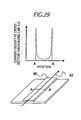
- Fig. 29 is a descriptive view of current concentration in the straight-shaped conductor line. As illustrated, a current concentrates on an edge in a straight-shaped conductor line 90 and distributes symmetrical with respect to a center axis 92 of the conductor line 90.
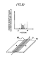
- Fig. 30 is a descriptive view of current concentration in the straight-shaped conductor line provided with slits.
- the slits are provided in the conductor line 90 to be symmetrical with respect to the center axis 92, whereby a current density distribution is uniformed.
- Fig. 31 is a descriptive view of current concentration in a conductor line having a bent portion in which a slit is formed.
- a current distribution becomes uneven from the outer-side to inner-side of the bent portion. That is, even if the slit symmetrically with respect to the center axis 92 is provided, the current concentration on inner-side edges of the bent portion of the conductor line, which is represented by the rightmost peak in a graph of Fig. 31 , can not be resolved.
- the large current density in the edges limits a loss property and a power handling.
- a resonator according to a first embodiment of the present invention is consists of a transmission line with a conductor line having a bent portion.
- a microstrip line in which a plurality of slits are formed in the conductor line along the extending direction thereof, and in which intervals of the slits become narrower toward the inner-side of the bent portion, is used as the transmission line.
- the slits which are narrower toward the inner-side of the bent portion, are provided in the transmission line, so that a current concentration on inner-side edges of the bent portion can be prevented and a high power handling and a low power loss of the resonator can be attained.
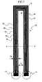
- Fig. 1 is a plan view showing a conductor line pattern of the resonator of the present embodiment.
- a microstrip line is used as the transmission line constituting the resonator.
- the drawing shows a top view of a substrate of a microstrip line, as viewed from above, wherein black-painted areas constitute the conductor line 10.
- the conductor line 10 has an angular-U hairpin shape.
- Five slits 20, 22, 24, 26, and 28 are provided in the bent portion of the hairpin resonator so as to extend from the neighborhood of one end 12 to the neighborhood of another end 14 along the direction of extension of the conductor line 10.
- the slit 20 is the outermost slit in the bent portion
- the slit 28 is the innermost slit of the bent portion.
- the intervals have a ratio of 3.4:2.8, a ratio of 2.8:2.2, and a ratio of 2.2:1.6 from the outer-side.
- a ratio of the width of the outermost line 30 to the width of the innermost line 32 is a ratio of 4:1.
- both ends 12 and 14 of the conductor line 10 are closed, namely, no slits are provided at both ends of the conductor line 10.
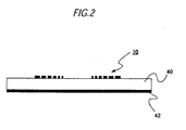
- Fig. 2 is a cross-sectional view of the resonator shown in Fig. 1 taken along line A-A' .
- the conductor line 10 shown in Fig. 1 is laid on an upper surface of a dielectric substrate 40.
- a ground plate 42 is formed of a conductive material on a lower surface of the dielectric substrate 40, thereby forming a microstrip line.
- the conductor line 10 is formed of, for instance, YBCO that is a superconducting material. For instance, sapphire is used for the dielectric substrate 40.
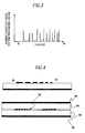
- Fig. 3 is a cross-sectional view of the resonator shown in Fig. 1 taken along line B-B' and a view showing the distribution of a current density achieved in the cross section of the resonator.
- a graph provided in an upper portion of Fig. 3 shows the distribution of a current density, wherein a vertical axis represents a current density and a horizontal axis represents a location.
- the current density on the inner-side of the bent portion (the B' side) is understood to be made uniform so as to become essentially identical with that on the outer-side of the bent portion.
- a simulation result acquired by an electromagnetic simulator show that a maximum current density of a hairpin resonator whose slits become narrower toward the inner-side of a bent portion comes to about one-third the maximum current density of a resonator having uniformly-spaced five slits.
- a resonance frequency is 800 MHz; the line width (W in Fig. 1 ) is 2 mm; a line interval (S in Fig. 1 ) is 2 mm; the slit width is 0.1 mm; and ratios of the slit intervals are the same as those achieved in Fig. 1 .
- the current concentration on a bent portion is significantly reduced. Therefore, a resonator exhibiting high power handling can be realized. Since a conductor loss in the bent portion is also diminished, a low-loss resonator can be implemented.
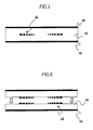
- Fig. 4 is a cross-sectional view of a resonator having a strip line structure that is a modification of the present embodiment.
- the strip line shown in Fig. 4 includes a second dielectric substrate 44 laid on the conductor line 10 and a second ground plane 46 formed on the second dielectric substrate 44.
- Fig. 5 is a cross-sectional view of a resonator having another-type strip line.
- the conductor line 10 is embedded in a dielectric 48, and the ground planes 42 and 46 are formed on the upper and lower surfaces of the dielectric 48.
- Fig. 6 is a cross-sectional view showing a method for manufacturing the another-type strip line structure.
- Two microstrip lines, each of which includes the conductor line 10, the dielectric substrate 40, and the ground plane 42 as shown in Fig. 2 are affixed together, thereby constituting a strip line.
- Such a strip line can also be used as the transmission line.
- the conductor line is shaped in the U shape.
- a radiation loss increases with an increase in frequency.
- the conductor line assume the U shape having one bent portion from a macroscopic viewpoint and two bent portions from a microscopic viewpoint.
- a bent portion is formed in a conductor line in order to mount a resonator in a limited size. Even in such a case, it is desirable to reduce the number of bent portions for minimizing a conductor loss.
- Fig. 7 is a plan view showing a conductor line pattern of a resonator that is a modification according to the first embodiment.
- the conductor line has the U shape. Specifically, as compared with the angular-U shape shown in Fig. 1 , the bent portion of the conductor line 10 has a circular-U shape. In contrast with the angular shape, the circular shape of the bent portion enables lessening of the current concentration on the bent portion.
- the effect of lessening the current concentration on the bent portion yielded by the present invention can also be yielded by varieties of resonators, so long as a conductor line is provided with a bent portion.
- angular-U and circular-U hairpin shapes are shown, various shapes having a single or a plurality of kinked or bent portions, such as a spiral shape, a meandering shape, the L shape, the M shape, the S shape, and an oval shape may be applied.
- the number of slits is also not limited to five, and an arbitrary number of slits is acceptable. However, as the number of slits increases, the number of boundary planes between a conductor section and an insulation section (an area which is not a conductor) also increases. Hence, when a design is conceived by use of, for instance, an electromagnetic simulator, computation involves consumption of much time. Therefore, the practical maximum number of slits is about 100, and, more preferably, ten slits or less are effective.
- both ends 12 and 14 of the conductor line 10 are closed. Specifically, no slits are formed ay both ends 12 and 14 of the conductor line 10 shown in Fig. 1 . If slits are formed up to the both ends, respective split conductor lines may function as a plurality of resonators, to thus cause an unwanted resonation mode. To suppress the unwanted resonationmode, the both ends are closed in the present embodiment.
- the embodiment has been described thus far by taking, as an example, the case where the conductor line is formed of a superconducting material.
- a conductor line is formed of a superconducting material
- the material of the conductor line is not limited to the superconducting material, and an arbitrary conductive material can also be applied to the conductor line.
- a resonator according to a second embodiment of the present invention is analogous to the resonator according to the first embodiment except the following features, and hence its explanations are omitted.
- the slit length ranges from 45 degrees to 90 degrees of an electrical length at a resonance frequency of the resonator. Essentially-center portions of the slits achieved in the lengthwise direction thereof are located in the center of the bent portion.
- An unwanted resonance mode can be avoided by reducing the slit length, while attaining the high power handling and the low conductor loss by relaxing a current concentration on a bent portion.
- Fig. 8 is a plan view showing a conductor line pattern of the resonator of the present embodiment.
- a microstrip line is used as in the first embodiment.
- the drawing is a view of a substrate of a microstrip line acquired when viewed from the direction of an upper surface thereof, and black-painted areas constitute the conductor line 10.
- the slits are limited solely to a neighborhood of the bent portion of the conductor line, for instance, a range of ⁇ 30 degrees (a total of 60 degrees) of an electrical length at the resonance frequency of the resonator. Further, the essentially-center portions of the slits achieved in the lengthwise direction thereof are placed in essentially the center of the bent portion.
- the center of the slits is described as the essentially-center portions is because, even when the center of the slits is not placed strictly in the center of the bent portion due to a machining error in regard to a design, or the like, the center can be deemed as being located substantially in the center and because working-effects similar to those yielded when the center of the slits are strictly located in the center of the bent portion can be yielded.
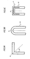
- Figs. 9A to 9C are views for describing the definition of the center of the bent portion.
- the word "center of the bent portion” means an area where an axis of symmetry A runs across the conductor line 10 when the conductor line 10 including the bent portion is essentially symmetrical as in the cases shown in Figs. 9A and 9B .
- slits of a desired electrical length cannot be designed because a plurality of slits overlap each other when the center of the bent portion determined by the above definition is used, as in the case where bent portions are continual.
- a virtual line segment L which has a desired electrical length and which runs the center and bent portion of a conductor line, is assumed as shown in Fig. 9C .
- an area where the axis of symmetry A of the line segment runs across the conductor line 10 is defined as the center of the bent portion.
- a resonator with slits induces occurrence of an unwanted resonance mode.
- the electrical length of the slit is preferably 90 degrees or less.
- the word "suppressing" means that an unwanted resonance mode is sufficiently moved away from a resonance mode used for constituting a filter to such an extent that an influence is not exerted in terms of a frequency axis.
- the resonator used for computation to be described below has the following sizes. Namely, the line width (W in Fig. 1 ) is 2 mm; a line interval (S in Fig. 1 ) is 2 mm; the slit width is 0.1 mm; and ratios of the slit intervals are the same as those shown in Fig. 1 .
- the resonator used for computation to be described below has the following sizes. Namely, the line width (W in Fig. 1 ) is 0.32 mm; a line interval (S in Fig. 1 ) is 0.32 mm; the slit width is 0.016 mm; and ratios of the slit intervals are the same as those shown in Fig. 1 .
- Fig. 10 shows an example 800-MHz-band hairpin-type resonator that has no slits, and the U shape.
- An upper figure shows a conductor line pattern of the resonator, and a lower figure shows a resonance characteristic.
- the horizontal axis represents a frequency
- the vertical axis represents a throughput (S21) acquired when the resonator is excited as a result of an input-output line being made close to the resonator.
- the drawing means that a resonance mode is present in frequencies at which peaks appear.
- a resonance peak is present in the vicinity of a frequency of 800 MHz and the vicinity of a frequency of 1500 MHz.
- a resonance peak appearing at 800 MHz is in a base resonance mode of half-wave resonance and used for a case where an 800-MHz-band filter is constituted by use of the resonator.
- a resonance peak appearing at 1500 MHz is a double wave of the frequency. The reason why the resonance peak is not accurately a double of the frequency is because an electrical length appears to differ between a case where adjacent currents are in phase with each other and a case where adjacent currents are out of phase with each other under influence of self-inductance. In the case of half-wave resonance, the adjacent currents are out of phase with each other.
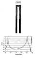
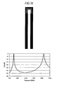
- Figs. 11 through 16 show a conductor line pattern and a resonance characteristic of an 800-MHz-band hairpin-type resonator acquired when the slit length is changed to 174 degrees, 115 degrees, 90 degrees, 55 degrees, 45 degrees, and 30 degrees of an electrical length.
- resonance modes which are not present in a slit-free resonator, are present in a range from 800 MHz to 1500 MHz.
- the resonance modes are those in which each of the slits acts as a resonator, and the slit length approximately corresponds to each resonance frequency.
- the resonance frequencies can be presumed to become higher than a frequency of 1500 MHz that is double-wave resonance (full-wave resonance).
- the slit length is reduced to electrical lengths of 90 degrees, 55 degrees, 45 degrees, and 30 degrees, unwanted resonance modes are not present in the range from 800 MHz to 1500 MHz.
- the 800-MHz-band resonator is mentioned as an example in the above. However, in order to conform whether or not the same results are yielded at another frequency band, the 5-GHz-band resonator was also subj ected to the same operations.
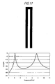
- Figs. 17 through 22 show results of the operations. A conductor line pattern of the resonator is provided in an upper portion of each of the drawings, and a resonance characteristic of the same is provided in a lower portion of each of the drawings.
- Fig. 17 shows a 5-GHz-band hairpin-type resonator that does not have any slits. Half-wave resonance appeared in the vicinity of 5 GHz, and full-wavelength resonance appeared in the vicinity of 8.8 GHz.
- Figs. 18 through 22 show results for the 5-GHz-band hairpin-type resonator acquiredwhen the slit length is changed to 175 degrees, 131 degrees, 90 degrees, 45 degrees, and 30 degrees of an electrical length.
- the slit length was changed to 175 degrees and 131 degrees, unwanted resonance modes are present in a range from 5 GHz to 8.8 GHz.
- the slit length was changed to 90 degrees, 45 degrees, and 30 degrees, an unwanted resonance mode is present in a frequency of 8.8 GHz or higher.
- a resonator with slits can be used, over a range from 800 MHz to 5 GHz, in the same manner as is a slitless resonator. From the results, similar results are readily conceived to be yielded by a resonator having a wider frequency range from, for instance, about 400 MHz that is one-half of 800 MHz to about 10 GHz that is twice as high as 5 GHz. Further, the shape of the resonator is not limited solely to a hairpin shape, but the present invention can also be applied to a resonator having the S shape, the M shape, or an oval shape. From the fact that unwanted resonance is generated by resonance corresponding to the length of slits, the essential requirement for such a case is readily conceived that the length of continual slits be set to 90 degrees or less.
- the electrical length of the slit be 45 degrees or more.
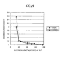
- Fig. 23 shows a relationship between a slit length (an electrical length or a degree) and the maximum current density of the resonator shown in Figs. 11 through 16 and that of the resonator shown in Figs. 18 through 22 .
- the maximum current density is a quantity standardized on the assumption that the maximum current density achieved at the longest slit length is taken as one.
- a solid line designates a result yielded by the 800-MHz-band resonator
- a dotted line designates a result yielded by the 5-GHz-band resonator. From the drawing, it is understood that, as the electrical length of the slit comes to a value of less than 45 degrees, the maximum current density abruptly increases, to thus lead to a reduction in the effect of the slits.
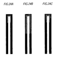
- Figs. 24A to 24C are descriptive views showing a relationship between a slit length and the maximum current density of a resonator.
- a high-current-density area in a U-shaped half-wave hairpin slitless resonator corresponds to the neighborhood of a shaded area provided on a resonator pattern shown in Fig. 24A .
- a current concentration on the shaded area can be dispersed by forming the slits, and the maximum current density can be reduced as shown in Fig. 24B .
- Fig. 24B Conversely, as shown in Fig.
- a threshold value of the slit length is conceived to be less than 45 degrees in terms of an electrical length. Since the 800-MHz-band resonator shows essentially the same tendency as that exhibited by the 5-GHz-band resonator. Hence, the same results are expected to be yielded by a resonator having a wider frequency range, for instance, from about 900 MHz (one-half 800 MHz) to about 10 GHz (twice 5 GHz).
- the resonator does not assume a hairpin shape but assumes a shape involving a large number of bent portions, such as the S shape, the M shape, and an oval shape, a location where a current is concentrated is dispersed, so that the threshold value of the slit length is conceived to become smaller than 45 degrees. Therefore, as long as the slit length is at least 45 degrees or longer, the effect for dispersing a current concentration is yielded.
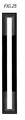
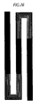
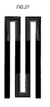
- Figs. 25 through 27 are plan views showing conductor line patterns of resonators of different shapes that are modifications of the present embodiment.
- Fig. 25 is an example in which the present embodiment is applied to an oval resonator
- Fig. 26 is an example in which the present embodiment is applied to an S-shaped resonator
- Fig. 27 is an example in which the present embodiment is applied to an M-shaped resonator.
- the present embodiment is not limited to these resonators.
- the present embodiment can also be applied to another resonator, so long as the resonator is made up of a transmission line having a conductor line pattern with bent portions.
- a filter according to a third embodiment of the present invention corresponds to a filter built from, for instance, a single or a plurality of resonators described in connection with the first and second embodiments.
- Fig. 28 is a plan view showing a conductor line pattern in the filter of the present embodiment.
- six resonators 60, 62, 64, 66, 68, and 70 are arranged in series, to thus constitute a six-stage Chebyshev filter, wherein the resonators have the same shape as that of the resonator shown in Fig. 8 .
- L-shaped conductor lines are arranged and are extended toward ends of a substrate, to thus constitute input and output feeders 72 and 74.
- the filter is built by use of low-loss, high-power-handling resonators, whereby a low-loss, high-power-handling filter can be implemented.
- the six-stage Chebyshev filter is described as an example, the present invention is not limited thereto. So long as a resonator is included, the present invention can be applied to various types of filters, such as a bandpass filter, a band-reject filter, a high-pass filter, a low-pass filter, and the like.
- a resonator and a filter in which a current distribution at the bent portion of the conductor line is uniformed to have a low loss property and a high-power handling.
Landscapes
- Physics & Mathematics (AREA)
- Electromagnetism (AREA)
- Control Of Motors That Do Not Use Commutators (AREA)
- Waveguides (AREA)
Claims (8)
- Résonateur comportant :une ligne de transmission (10) comportant une ligne conductrice avec une partie courbée,dans lequel la ligne conductrice possède une pluralité de fentes (20, 22, 24, 26, 28) formées dans celle-ci, les fentes étant formées dans une direction d'extension de la ligne conductrice pour traverser la partie courbée, et caractérisé en ce que les fentes sont formées pour présenter des intervalles entre des fentes adjacentes, notamment, la largeur des lignes prises en sandwich entre les fentes, qui se rétrécissent du côté extérieur vers le côté intérieur de la partie courbée.
- Résonateur selon la revendication 1,
dans lequel les fentes ne sont pas prévues aux deux extrémités de la ligne conductrice. - Résonateur selon la revendication 1 ou 2,
dans lequel les fentes sont formées pour présenter une longueur électrique de 45 degrés à 90 degrés à une fréquence de résonance du résonateur, et
dans lequel les fentes sont formées de sorte qu'un centre longitudinal des fentes est positionné presque à la même position avec un centre longitudinal de la partie courbée. - Résonateur selon la revendication 1, 2 ou 3,
dans lequel la ligne conductrice présente une forme en U angulaire. - Résonateur selon la revendication 1, 2 ou 3,
dans lequel la ligne conductrice possède une forme en U circulaire. - Résonateur selon l'une quelconque des revendications précédentes,
dans lequel la ligne conductrice est formée en un matériau supraconducteur. - Résonateur selon l'une quelconque des revendications précédentes,
dans lequel la ligne de transmission comporte :une ligne ruban ; ouune ligne micro ruban. - Filtre comportant le résonateur selon l'une quelconque des revendications précédentes.
Applications Claiming Priority (1)
| Application Number | Priority Date | Filing Date | Title |
|---|---|---|---|
| JP2007304571A JP4489113B2 (ja) | 2007-11-26 | 2007-11-26 | 共振器およびフィルタ |
Publications (2)
| Publication Number | Publication Date |
|---|---|
| EP2065965A1 EP2065965A1 (fr) | 2009-06-03 |
| EP2065965B1 true EP2065965B1 (fr) | 2013-06-19 |
Family
ID=40456255
Family Applications (1)
| Application Number | Title | Priority Date | Filing Date |
|---|---|---|---|
| EP08253812.5A Ceased EP2065965B1 (fr) | 2007-11-26 | 2008-11-26 | Résonateur et filtre |
Country Status (3)
| Country | Link |
|---|---|
| US (1) | US7983728B2 (fr) |
| EP (1) | EP2065965B1 (fr) |
| JP (1) | JP4489113B2 (fr) |
Families Citing this family (11)
| Publication number | Priority date | Publication date | Assignee | Title |
|---|---|---|---|---|
| JP5419088B2 (ja) * | 2010-01-07 | 2014-02-19 | アルパイン株式会社 | 基板減衰回路 |
| JP5349612B2 (ja) * | 2010-03-12 | 2013-11-20 | 株式会社東芝 | 通信装置 |
| FR2977382A1 (fr) * | 2011-06-29 | 2013-01-04 | Thomson Licensing | Filtre stop bande a rejection elevee et duplexeur utilisant de tels filtres |
| US20130328645A1 (en) * | 2012-06-08 | 2013-12-12 | International Business Machines Corporation | Plating Stub Resonance Shift with Filter Stub Design Methodology |
| JP5780524B2 (ja) * | 2012-08-07 | 2015-09-16 | 国立大学法人山梨大学 | ダブルストリップ共振器 |
| JP6265460B2 (ja) * | 2013-06-01 | 2018-01-24 | 国立大学法人山梨大学 | デュアルバンド共振器及びそれを用いたデュアルバンド帯域通過フィルタ |
| JP6265461B2 (ja) * | 2013-07-04 | 2018-01-24 | 国立大学法人山梨大学 | 共振器装荷型デュアルバンド共振器及びそれを用いたデュアルバンドフィルタ |
| CN204696222U (zh) | 2013-08-02 | 2015-10-07 | 株式会社村田制作所 | 高频信号传输线路及电子设备 |
| JP6265478B2 (ja) * | 2014-01-29 | 2018-01-24 | 国立大学法人山梨大学 | チューナブルデュアルバンド帯域通過フィルタ |
| JP6236701B2 (ja) * | 2014-12-09 | 2017-11-29 | 国立大学法人山梨大学 | 改良型チューナブルデュアルバンド帯域通過フィルタ |
| JP6913505B2 (ja) | 2017-05-01 | 2021-08-04 | 東京計器株式会社 | デュアルバンド共振器、及び、それを用いたデュアルバンド帯域通過フィルタ |
Family Cites Families (8)
| Publication number | Priority date | Publication date | Assignee | Title |
|---|---|---|---|---|
| JP3587264B2 (ja) | 1993-09-22 | 2004-11-10 | 株式会社村田製作所 | ストリップ線路とそれを用いる伝送線路,共振器およびフィルタ |
| CA2148341C (fr) | 1995-05-01 | 1997-02-04 | Shen Ye | Methode et structure utilisant des rubans separes par un espace pour lignes de transmission haute tension a supraconducteur a haute temperature |
| JP2894245B2 (ja) | 1995-05-26 | 1999-05-24 | 株式会社移動体通信先端技術研究所 | 高周波伝送線路 |
| US5909087A (en) | 1996-03-13 | 1999-06-01 | Lutron Electronics Co. Inc. | Lighting control with wireless remote control and programmability |
| US5888942A (en) | 1996-06-17 | 1999-03-30 | Superconductor Technologies, Inc. | Tunable microwave hairpin-comb superconductive filters for narrow-band applications |
| JPH11177310A (ja) * | 1997-10-09 | 1999-07-02 | Murata Mfg Co Ltd | 高周波伝送線路、誘電体共振器、フィルタ、デュプレクサおよび通信機 |
| JP3391271B2 (ja) * | 1998-09-01 | 2003-03-31 | 株式会社村田製作所 | 高周波用低損失電極 |
| JP4822970B2 (ja) | 2006-07-27 | 2011-11-24 | 富士通株式会社 | 分割型マイクロストリップライン共振器およびこれを用いたフィルタ |
-
2007
- 2007-11-26 JP JP2007304571A patent/JP4489113B2/ja active Active
-
2008
- 2008-11-25 US US12/323,255 patent/US7983728B2/en active Active
- 2008-11-26 EP EP08253812.5A patent/EP2065965B1/fr not_active Ceased
Also Published As
| Publication number | Publication date |
|---|---|
| US20090146762A1 (en) | 2009-06-11 |
| US7983728B2 (en) | 2011-07-19 |
| JP2009130699A (ja) | 2009-06-11 |
| JP4489113B2 (ja) | 2010-06-23 |
| EP2065965A1 (fr) | 2009-06-03 |
Similar Documents
| Publication | Publication Date | Title |
|---|---|---|
| EP2065965B1 (fr) | Résonateur et filtre | |
| JP4309902B2 (ja) | 共振回路、フィルタ回路及びアンテナ装置 | |
| US6686808B1 (en) | Coplanar stripline with corrugated structure | |
| KR101140143B1 (ko) | 다중 대역저지 기능을 갖는 초광대역 안테나 및 그 설계 방법 | |
| US20040233022A1 (en) | Resonator and filter comprising the same | |
| EP1128460B1 (fr) | Filtre passe-bande à double mode | |
| US10128552B2 (en) | Structure and electronic circuit | |
| WO1999056338A1 (fr) | Circuit hyperfrequence coplanaire a suppression de modes indesirables | |
| US7084813B2 (en) | Antennas with reduced space and improved performance | |
| US5922650A (en) | Method and structure for high power HTS transmission lines using strips separated by a gap | |
| EP0841712B1 (fr) | Filtre du type de ligne à constantes distribuées | |
| CN104269588B (zh) | 一种基于中心枝节加载的小型化六边形三模滤波器 | |
| US5160906A (en) | Microstripe filter having edge flared structures | |
| JP2014036258A (ja) | マルチバンド帯域通過フィルタ | |
| EP1530257A1 (fr) | Antenne planaire bi-bande | |
| US6650914B2 (en) | High frequency super conductive filter | |
| US9722307B2 (en) | Terminal antenna structure and terminal | |
| KR100521895B1 (ko) | 인덕턴스 성분의 식각된 홀을 이용한 씨피더블유 저역통과필터 | |
| US6566987B2 (en) | Dielectric filter, dielectric duplexer, and communication apparatus | |
| US10165674B1 (en) | Circuit board and electromagnetic bandgap structure thereof | |
| JP2894245B2 (ja) | 高周波伝送線路 | |
| US6496710B1 (en) | Signal filter having circularly arranged resonators | |
| JP6151071B2 (ja) | フィルタおよび共振器 | |
| US6934569B2 (en) | Elliptical resonators with radial current mode and radio frequency filter formed therefrom | |
| US20010006360A1 (en) | Microwave filter |
Legal Events
| Date | Code | Title | Description |
|---|---|---|---|
| PUAI | Public reference made under article 153(3) epc to a published international application that has entered the european phase |
Free format text: ORIGINAL CODE: 0009012 |
|
| 17P | Request for examination filed |
Effective date: 20081202 |
|
| AK | Designated contracting states |
Kind code of ref document: A1 Designated state(s): AT BE BG CH CY CZ DE DK EE ES FI FR GB GR HR HU IE IS IT LI LT LU LV MC MT NL NO PL PT RO SE SI SK TR |
|
| AX | Request for extension of the european patent |
Extension state: AL BA MK RS |
|
| AKX | Designation fees paid |
Designated state(s): DE FR GB |
|
| GRAP | Despatch of communication of intention to grant a patent |
Free format text: ORIGINAL CODE: EPIDOSNIGR1 |
|
| GRAS | Grant fee paid |
Free format text: ORIGINAL CODE: EPIDOSNIGR3 |
|
| GRAA | (expected) grant |
Free format text: ORIGINAL CODE: 0009210 |
|
| AK | Designated contracting states |
Kind code of ref document: B1 Designated state(s): DE FR GB |
|
| REG | Reference to a national code |
Ref country code: GB Ref legal event code: FG4D |
|
| REG | Reference to a national code |
Ref country code: DE Ref legal event code: R096 Ref document number: 602008025409 Country of ref document: DE Effective date: 20130814 |
|
| PLBE | No opposition filed within time limit |
Free format text: ORIGINAL CODE: 0009261 |
|
| STAA | Information on the status of an ep patent application or granted ep patent |
Free format text: STATUS: NO OPPOSITION FILED WITHIN TIME LIMIT |
|
| 26N | No opposition filed |
Effective date: 20140320 |
|
| REG | Reference to a national code |
Ref country code: DE Ref legal event code: R097 Ref document number: 602008025409 Country of ref document: DE Effective date: 20140320 |
|
| REG | Reference to a national code |
Ref country code: FR Ref legal event code: PLFP Year of fee payment: 8 |
|
| REG | Reference to a national code |
Ref country code: FR Ref legal event code: PLFP Year of fee payment: 9 |
|
| REG | Reference to a national code |
Ref country code: FR Ref legal event code: PLFP Year of fee payment: 10 |
|
| REG | Reference to a national code |
Ref country code: FR Ref legal event code: PLFP Year of fee payment: 11 |
|
| PGFP | Annual fee paid to national office [announced via postgrant information from national office to epo] |
Ref country code: FR Payment date: 20221010 Year of fee payment: 15 |
|
| PGFP | Annual fee paid to national office [announced via postgrant information from national office to epo] |
Ref country code: GB Payment date: 20221006 Year of fee payment: 15 Ref country code: DE Payment date: 20221004 Year of fee payment: 15 |
|
| REG | Reference to a national code |
Ref country code: DE Ref legal event code: R119 Ref document number: 602008025409 Country of ref document: DE |
|
| GBPC | Gb: european patent ceased through non-payment of renewal fee |
Effective date: 20231126 |
|
| PG25 | Lapsed in a contracting state [announced via postgrant information from national office to epo] |
Ref country code: DE Free format text: LAPSE BECAUSE OF NON-PAYMENT OF DUE FEES Effective date: 20240601 |
|
| PG25 | Lapsed in a contracting state [announced via postgrant information from national office to epo] |
Ref country code: GB Free format text: LAPSE BECAUSE OF NON-PAYMENT OF DUE FEES Effective date: 20231126 |
|
| PG25 | Lapsed in a contracting state [announced via postgrant information from national office to epo] |
Ref country code: FR Free format text: LAPSE BECAUSE OF NON-PAYMENT OF DUE FEES Effective date: 20231130 |
|
| PG25 | Lapsed in a contracting state [announced via postgrant information from national office to epo] |
Ref country code: GB Free format text: LAPSE BECAUSE OF NON-PAYMENT OF DUE FEES Effective date: 20231126 Ref country code: FR Free format text: LAPSE BECAUSE OF NON-PAYMENT OF DUE FEES Effective date: 20231130 Ref country code: DE Free format text: LAPSE BECAUSE OF NON-PAYMENT OF DUE FEES Effective date: 20240601 |