EP2066021A2 - Steuervorrichtung von mehrphasigem Elektromotor - Google Patents
Steuervorrichtung von mehrphasigem Elektromotor Download PDFInfo
- Publication number
- EP2066021A2 EP2066021A2 EP08169611A EP08169611A EP2066021A2 EP 2066021 A2 EP2066021 A2 EP 2066021A2 EP 08169611 A EP08169611 A EP 08169611A EP 08169611 A EP08169611 A EP 08169611A EP 2066021 A2 EP2066021 A2 EP 2066021A2
- Authority
- EP
- European Patent Office
- Prior art keywords
- phase
- pwm signal
- current
- electric motor
- duty
- Prior art date
- Legal status (The legal status is an assumption and is not a legal conclusion. Google has not performed a legal analysis and makes no representation as to the accuracy of the status listed.)
- Granted
Links
- 238000001514 detection method Methods 0.000 claims abstract description 115
- 230000007274 generation of a signal involved in cell-cell signaling Effects 0.000 claims abstract description 20
- 230000008859 change Effects 0.000 claims abstract description 10
- 239000013598 vector Substances 0.000 description 64
- 238000006243 chemical reaction Methods 0.000 description 53
- 238000000034 method Methods 0.000 description 17
- 238000005259 measurement Methods 0.000 description 11
- 230000008929 regeneration Effects 0.000 description 11
- 238000011069 regeneration method Methods 0.000 description 11
- 230000010363 phase shift Effects 0.000 description 10
- 238000010586 diagram Methods 0.000 description 7
- 230000008569 process Effects 0.000 description 6
- 230000008901 benefit Effects 0.000 description 3
- 238000012937 correction Methods 0.000 description 2
- 230000000694 effects Effects 0.000 description 2
- 230000010354 integration Effects 0.000 description 2
- 230000002265 prevention Effects 0.000 description 2
- 230000001934 delay Effects 0.000 description 1
- 230000003111 delayed effect Effects 0.000 description 1
- 230000001419 dependent effect Effects 0.000 description 1
- 230000005685 electric field effect Effects 0.000 description 1
- 230000004907 flux Effects 0.000 description 1
- 230000006698 induction Effects 0.000 description 1
- 238000012544 monitoring process Methods 0.000 description 1
- 238000012545 processing Methods 0.000 description 1
- 230000009467 reduction Effects 0.000 description 1
- 230000004044 response Effects 0.000 description 1
- 238000000926 separation method Methods 0.000 description 1
- 230000001360 synchronised effect Effects 0.000 description 1
- 238000004804 winding Methods 0.000 description 1
Images





Classifications
-
- H—ELECTRICITY
- H02—GENERATION; CONVERSION OR DISTRIBUTION OF ELECTRIC POWER
- H02P—CONTROL OR REGULATION OF ELECTRIC MOTORS, ELECTRIC GENERATORS OR DYNAMO-ELECTRIC CONVERTERS; CONTROLLING TRANSFORMERS, REACTORS OR CHOKE COILS
- H02P27/00—Arrangements or methods for the control of AC motors characterised by the kind of supply voltage
- H02P27/04—Arrangements or methods for the control of AC motors characterised by the kind of supply voltage using variable-frequency supply voltage, e.g. inverter or converter supply voltage
- H02P27/06—Arrangements or methods for the control of AC motors characterised by the kind of supply voltage using variable-frequency supply voltage, e.g. inverter or converter supply voltage using DC to AC converters or inverters
- H02P27/08—Arrangements or methods for the control of AC motors characterised by the kind of supply voltage using variable-frequency supply voltage, e.g. inverter or converter supply voltage using DC to AC converters or inverters with pulse width modulation
-
- H—ELECTRICITY
- H02—GENERATION; CONVERSION OR DISTRIBUTION OF ELECTRIC POWER
- H02P—CONTROL OR REGULATION OF ELECTRIC MOTORS, ELECTRIC GENERATORS OR DYNAMO-ELECTRIC CONVERTERS; CONTROLLING TRANSFORMERS, REACTORS OR CHOKE COILS
- H02P29/00—Arrangements for regulating or controlling electric motors, appropriate for both AC and DC motors
- H02P29/50—Reduction of harmonics
-
- H—ELECTRICITY
- H02—GENERATION; CONVERSION OR DISTRIBUTION OF ELECTRIC POWER
- H02M—APPARATUS FOR CONVERSION BETWEEN AC AND AC, BETWEEN AC AND DC, OR BETWEEN DC AND DC, AND FOR USE WITH MAINS OR SIMILAR POWER SUPPLY SYSTEMS; CONVERSION OF DC OR AC INPUT POWER INTO SURGE OUTPUT POWER; CONTROL OR REGULATION THEREOF
- H02M1/00—Details of apparatus for conversion
- H02M1/0003—Details of control, feedback or regulation circuits
- H02M1/0009—Devices or circuits for detecting current in a converter
-
- H—ELECTRICITY
- H02—GENERATION; CONVERSION OR DISTRIBUTION OF ELECTRIC POWER
- H02M—APPARATUS FOR CONVERSION BETWEEN AC AND AC, BETWEEN AC AND DC, OR BETWEEN DC AND DC, AND FOR USE WITH MAINS OR SIMILAR POWER SUPPLY SYSTEMS; CONVERSION OF DC OR AC INPUT POWER INTO SURGE OUTPUT POWER; CONTROL OR REGULATION THEREOF
- H02M7/00—Conversion of AC power input into DC power output; Conversion of DC power input into AC power output
- H02M7/42—Conversion of DC power input into AC power output without possibility of reversal
- H02M7/44—Conversion of DC power input into AC power output without possibility of reversal by static converters
- H02M7/48—Conversion of DC power input into AC power output without possibility of reversal by static converters using discharge tubes with control electrode or semiconductor devices with control electrode
- H02M7/53—Conversion of DC power input into AC power output without possibility of reversal by static converters using discharge tubes with control electrode or semiconductor devices with control electrode using devices of a triode or transistor type requiring continuous application of a control signal
- H02M7/537—Conversion of DC power input into AC power output without possibility of reversal by static converters using discharge tubes with control electrode or semiconductor devices with control electrode using devices of a triode or transistor type requiring continuous application of a control signal using semiconductor devices only, e.g. single switched pulse inverters
- H02M7/539—Conversion of DC power input into AC power output without possibility of reversal by static converters using discharge tubes with control electrode or semiconductor devices with control electrode using devices of a triode or transistor type requiring continuous application of a control signal using semiconductor devices only, e.g. single switched pulse inverters with automatic control of output wave form or frequency
- H02M7/5395—Conversion of DC power input into AC power output without possibility of reversal by static converters using discharge tubes with control electrode or semiconductor devices with control electrode using devices of a triode or transistor type requiring continuous application of a control signal using semiconductor devices only, e.g. single switched pulse inverters with automatic control of output wave form or frequency by pulse-width modulation
Definitions
- the present invention relates to a pulse width modulation (PWM) drive control of a multi-phase electric motor such as a three-phase brushless motor.
- PWM pulse width modulation
- the present invention relates to a noise prevention technique of a controller of a multi-phase electric motor arranged with a single current detector between a drive circuit for PWM driving and a direct current (DC) power supply (high voltage side or low voltage side).
- DC direct current
- a PWM signal for determining ON/OFF timing of a switching element for driving the multi-phase electric motor is generated by comparing a carrier wave of saw-tooth shape or triangular shape (saw-tooth signal, triangular signal) and a duty set value corresponding to a target current value in each phase of the multi-phase electric motor. That is, whether the PWM signal is high level or low level is determined depending on whether a value (value of PWM counter) of the saw-tooth signal or the triangular signal is greater than or equal to, or smaller than a duty set value.
- the time interval in time of switching between one phase and another phase sometimes becomes very small in the controller of the multi-phase electric motor for generating the PWM signal based on the saw-tooth signal and the triangular signal, and driving the multi-phase electric motor.
- the current is not stable due to the switching time of an electric field effect transistor of the drive circuit, the presence of dead zone (dead time), and also the response delay of an electronic processing circuit, the measurement of an accurate current value by a current detector cannot be carried out during such a period.
- an accurate current value cannot be detected unless a stable signal is continuously inputted for at least 2 ⁇ s according to the specification of the A/D converter. If the input signal is not stably inputted continuously for 2 ⁇ s, the A/D converter cannot detect an accurate current value of each phase.
- a single current sensor for detecting the current value flowing through a current path is arranged on the current path between a motor drive circuit and a ground, and a phase of a saw-tooth wave for generating the PWM signal of each phase is shifted to shift the timing of fall of the PWM signal of each phase to the low level.
- a value of a U-phase current flowing through the electric motor is then obtained based on an output signal of the current sensor during a period in which a predetermined time has elapsed from when the PWM signal of a V phase fell to the low level.
- a total current value of the U-phase current and a V-phase current flowing through the electric motor is obtained based on an output signal of the current sensor during a period in which a predetermined time has elapsed from when the PWM signal of a W phase fell to the low level.
- a drive system for a three-phase brushless AC motor described in Japanese Unexamined Patent Publication No. 2005-531270 is configured to optimize a transistor switching pattern in order to enhance the power output while enabling the measurement of the current in all phases using a single sensor. This is realized by defining a voltage demand vector x in a case where three or more states are required to satisfy a minimum state time requirement determined by the single sensor method, and calculating the three or more state vectors for generating the request vector x while still allowing the single current detection.
- a triangular signal is used for a carrier wave, terms h phase, m phase, and I phase are used in place of the terms U phase, V phase, and W phase, where the time interval between the h phase and the m phase is represented as t1 and the time interval between the m phase and the I phase is represented as t2.
- the process of Case 2 is performed when the time intervals t1, t2 are both smaller than a threshold value (mw).
- the process of Case 3 or Case 4 is performed when either one of the time intervals t1, t2 is smaller than the threshold value (mw). In the case of the process of Case 2 (see FIG.
- the Duty maximum phase is shifted to the left side, and the Duty minimum phase is shifted to the right side (see FIG. 12B ). If in the case of the process of Case 3 (see FIG. 15 ), and determined that only one phase needs to be shifted (N of step 148), the Duty maximum phase is shifted to the left side (see FIG. 14B ). If in the case of the process of Case 4 (see FIG. 17), and determined that only one phase needs to be shifted (N of step 166), the Duty minimum phase is shifted to the left side (see FIG. 16B ).
- the time interval in time of switching between one phase and another phase becomes small, the time interval in time of switching between one phase and another phase becomes large by performing a correction of shifting the phase of a predetermined phase, and an accurate current value of each phase of the multi-phase electric motor can be detected using the single current detector.
- the frequency of the ON/OFF of the switching element for driving the multi-phase electric motor is included within an audible frequency, it is heard by the user as noise and gives the user an unpleasant feeling.
- a control frequency and the corrected current ripple frequency are the same when the PWM signal is corrected.
- a control cycle time is 400 ⁇ s, and thus the control frequency and the corrected current ripple frequency become 2.5 kHz.
- the current ripple is generated in time of switching by turning ON/OFF the switching element based on the corrected PWM signal.
- the frequency of the current ripple becomes the same as the control frequency, where if the relevant frequency is included in an audible range, it is heard by the user as noise and gives the user an unpleasant feeling.
- a motor drive device of an electric power steering described in Japanese Patent No. 2540140 assumes one switching element of each pair for conduction holding and the other switching element for high-speed switching of the switching elements of two pairs, and has the frequency of a pulse width modulation signal for high-speed switching higher than an audible frequency region, and thus the linearity of the output torque of the motor with respect to a steering torque can be enhanced by effectively utilizing a current continuation effect by a flywheel diode, and the generation of vibration sound can be prevented regardless of the switching by the pulse width modulation signal.
- An inverter device described in Japanese Unexamined Patent Publication No. 63-73898 generates the PWM signal by comparing a modulation wave signal obtained by amplifying an error of a magnetic flux command signal of the frequency proportional to a frequency command from the outside and a motor voltage integration signal outputted by an integration circuit for integrating an inverter output voltage, and a triangular signal which is the carrier frequency of a non-audible frequency.
- a controller of an electric vehicle described in Japanese Unexamined Patent Publication No. 9-191508 drives a motor with the power of a battery by PWM controlling an inverter arranged between a battery and a motor with PWM control means, and normally sets the frequency of the PWM control means higher than an audible frequency to reduce the switching noise of the inverter.
- motor operation state detection means detects that the motor is in a low-speed, high-load operation state, and there is a possibility the switching element of the inverter may overheat
- frequency changing means lowers the frequency of the PWM control means to prevent damage by overheat of the switching element of the inverter.
- controller of a multi-phase electric motor capable of generating the PWM signal based on the saw-tooth signal or the triangular signal, and accurately detecting the current value of each phase for every control period using signal current detection means, and having a sufficient noise prevention effect.
- FIG. 15 shows a diagram showing the control method of Japanese Unexamined Patent Publication No. 10-155278 of the prior art, and is a timing chart in a case where two phases in one control period are not detectable.
- One control period is 400 ⁇ sec, and the configuration thereof is five periods of the PWM signal based on the saw-tooth signal of 80 ⁇ sec period.
- the switching time intervals between the V phase and the W phase, and between the U phase and the W phase thus become large, and the accurate current value of the V phase is detected in a measurement period U2, and of the U phase is detected in a measurement period U1.
- the phase of the PWM signal of the V phase of minimum phase is made long (compensation period U2) and the phase of the PWM signal of the U phase of maximum phase is made short (compensation period U1) to compensate for the amount of change of the phase in the first period.
- FIG. 16 shows a diagram showing the control method of Japanese Unexamined Patent Publication No. 10-155278 of the prior art, and is a timing chart in a case where two phases in three control periods are not detectable.
- the period of the current ripple within the first period represented in the shunt waveform in each control period is the same as the control cycle time 400 ⁇ sec of one control period, and the frequency corresponding to such a period is in the audible range. Therefore, the noise generates.
- a controller of a multi-phase electric motor includes drive means, including a pair of an upper arm switching element and a lower arm switching element, for driving the multi-phase electric motor; single current detection means for detecting a current value of the multi-phase electric motor; PWM signal generation means for generating plural PWM signals of each phase within one control period based on the current value detected by the current detection means and a carrier signal; current detectability determination means for determining whether or not the current value is detectable in the current detection means based on the PWM signal of each phase generated by the PWM signal generation means; and phase movement means for moving a phase of the PWM signal of a predetermined phase generated by the PWM signal generation means by a predetermined amount when the current detectability determination means determines that current is not detectable.
- the current value of each phase can be accurately detected for every control period using the single current detection means, and the phase movement means moves the phase of the PWM signal of the predetermined phase by a predetermined amount when the current is not detectable, and thus the generation of noise can be prevented in such a manner that the frequency of the current ripple by switching based on the PWM signal is not included in the audible range by such movement.
- the phase movement means may move the phase by a predetermined amount for all the PWM signals of the predetermined phase in one control period.
- the one control period is normally a few hundred ⁇ sec., one control period is configured by few PWM signals, and the control cycle time is a few dozen ⁇ sec, and thus the frequency of the current ripple by switching becomes a frequency higher than the audible frequency region, and thus is not included in the audible range, whereby the generation of noise can be prevented.
- the controller of the multi-phase electric motor further includes switching number determination means for determining whether or not number of the upper arm switching element to turn ON is an even number or an odd number when the current detectability determination means determines that current is not detectable, wherein the phase movement means may move the phase of the PWM signal of the predetermined phase generated by the PWM signal generation means by a predetermined amount based on the determination result of the switching number determination means.
- the generation of noise can be prevented, and furthermore, the current value of each phase can be accurately detected for every control period using the single current detection means without changing the duty of each phase even if the time interval of the switching between a predetermined phase and another phase is originally short to an extent the current value cannot be detected since the time interval of the switching between the predetermined phase in which the phase is moved and another phase becomes large, and the current value can be detected with the current value of the moved predetermined phase stabilized.
- the present invention may adopt a configuration of including drive means, including a pair of an upper arm switching element and a lower arm switching element, for driving the multi-phase electric motor; single current detection means for detecting a current value of the multi-phase electric motor; PWM signal generation means for generating plural PWM signals of each phase within one control period based on the current value detected by the current detection means and a carrier signal; and phase movement means for moving a phase of the PWM signal by a predetermined amount such that frequency in change of the PWM signal of the predetermined phase generated by the PWM signal generation means is included in a non-audible range.
- the current value of each phase can be accurately detected for every control period using the single current detection means, and the generation of noise can be prevented as the frequency of the current ripple by switching based on the PWM signal is not included in the audible range since the phase movement means moves the phase such that the frequency of change of the PWM signal of the predetermined phase is included in the non-audible range.
- the current value of each phase can be accurately detected for every control period using the single current detection means, and the generation of noise can be prevented by causing the phase movement means to move the phase of the PWM signal of the predetermined phase by a predetermined amount such that the frequency of the current ripple by switching based on the PWM signal is not included in the audible range.
- FIG. 1 shows a block diagram of a controller of a multi-phase electric motor according to an embodiment of the present invention.
- a controller 1 of a multi-phase electric motor 7 according to the embodiment of the present invention has the following configuration.
- Drive means 6 is connected between a power supply and a ground, as hereinafter described in the description of a circuit diagram of FIG. 2 , includes a pair of upper arm switching elements Q1 to Q3 and lower arm switching elements Q4 to Q6, and drives the multi-phrase electric motor 7.
- Current detection means 8 is connected between the drive means 6 and a ground, and detects a current value flowing to the multi-phase electric motor 7 at a predetermined time.
- PWM signal generation means 2 generates PWM signal of each phase based on the current value detected in the current detection means 8 and the saw-tooth signal having a predetermined frequency.
- Current detectability determination means 3 determines whether or not the current value is detectable in the current detection means 8, that is, whether or not there is a switching time interval for the accurate current value to be detected in the current detection means 8 based on the PWM signal of each phase generated in the PWM signal generation means 2.
- Switching number determination means 4 determines whether or not the number of switching elements turned ON of the three upper arm switching elements Q1 to Q3 is an even number when the current detectability determination means 3 determines that the current is not detectable.
- Phase movement means 5 advances or delays the phase of the PWM signal of the predetermined phase generated by the PWM signal generation means 2 by a predetermined amount based on the determination result of the switching number determination means 4, and outputs the PWM signal which phase is moved to the drive means 6.
- Current detection period determination means 10 determines a current detection start timing and a current detection period by the current detection means 8 based on a fall time of the PWM signal of each phase determined in the phase movement means 5.
- Each phase current calculation means 9 calculates the current value of the remaining phase that cannot be directly detected based on the current value detected in the current detection means 8 and the PWM signal generated in the PWM signal generation means 2.
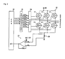
- FIG. 2 shows a circuit diagram of the controller 1 of the multi-phase electric motor according to the embodiment of the present invention.
- a CPU 22 outputs each PWM signal of the U phase upper stage, the V phase upper stage, and the W phase upper stage to a dead time generation block 23.
- the dead time generation block 23 inputs such signals, provides a slight time interval in which the signals for the upper arm switching elements Q1 to Q3 and the lower arm switching elements Q4 to Q6 of each phase are turned OFF such that the signals for the upper arm switching elements Q1 to Q3 and the lower arm switching elements Q4 to Q6 of each phase both are not turned ON for circuit protection, generates each PWM signal of the U phase upper stage, the U phase lower stage, the V phase upper stage, the V phase lower stage, the W phase upper stage, and the W phase lower stage and outputs the PWM signals to a driver IC 24.
- the function of the dead time generation block 23 may be realized by software in the CPU 22.
- the driver IC 24 inputs such signals to control an FET bridge 25.
- the FET bridge 25 is connected between a power supply VR and the ground, and includes three pairs of the upper arm switching elements Q1 to Q3 and the lower arm switching elements Q4 to Q6. An intermediate part of the three pairs of the upper arm switching elements Q1 to Q3 and the lower arm switching elements Q4 to Q6 is connected to each phase of the three-phase electric motor.
- a single shunt resistor 26 is connected between the FET bridge 25 and the ground. The voltage over both ends of the shunt resistor 26 is inputted to an A/D conversion port of the CPU 22 via a current detection circuit 27 including an operational amplifier, a resistor, and the like.
- the basic function of the present circuit is as described below.
- the phase current detection period is 250 ⁇ sec
- the detection method is two-phase detection/one-phase estimation method
- the PWM mode is a saw-tooth PWM.
- the CPU 22 configures the current detectability determination means 3, the switching number determination means 4, the phase movement means 5, each phase current calculation means 9, and the current detection period determination means 10 in FIG. 1
- the CPU 22 and the dead time generation block 23 configure the PWM signal generation means 2 in FIG. 1
- the FET bridge 25 configures the drive means 6 in FIG. 1
- the shunt resistor 26 and the current detection circuit 27 configure the current detection means 8 in FIG. 1 .
- the three-phase electric motor is used for the multi-phase electric motor 7 of FIG. 1 .
- the three-phase electric motor is a brushless motor used in an electrical power steering device of the vehicle, and the like.
- FIG. 3 shows a flowchart of the controller 1 of the multi-phase electric motor according to the embodiment of the present invention.
- the PWM signal generation means 2 determines a PWM command value of each phase of U, V, and W (S1). As the details will be hereinafter described, pattern determination is performed based on the duty of each phase of U, V, and W (S2). The separation of cases of detectability by the current detectability determination means 3 is then carried out (S3 to S5). First, whether or not two phases of the three phases are detectable is determined (S3). If two phases are not detectable (No in S3), whether or not one phase of the three phases is detectable is determined (S4).
- the switching number determination means 4 determines whether an even number vector is detectable (S5). If the even number vector is not detectable (No in S5), an odd number vector is detectable.
- the even number vector and the odd number vector will be hereinafter described. With respect to a certain phase, the current detection on such a phase is possible if there is a switching time enough for an accurate current value to be detected in the CPU 22.
- the phase movement means 5 calculates the phase that requires movement and the necessary amount of shift based on the detectability determination condition. First, if two phases are detectable (Yes in S3), the movement is not necessary, and the phase shift amount of each phase of PWM may be zero (S6). If only the even number vector is detectable (Yes in S5), the phase of the phase having a maximum duty is delayed, and the shift amount thereof is calculated (S7). If only the odd number vector is detectable (No in S5), the phase of the phase having a minimum duty is advanced, and the shift amount thereof is calculated (S8). If no phase is detectable (No in S4), the phase of the phase having a maximum duty and the phase of the phase having a minimum duty are both shifted, and the respective shift amount are calculated (S9).
- the current detection period determination means 10 determines the current detection start timing by the current detection means 8 based on the fall time of the PWM signal of each phase determined by the phase movement means 5 (S10).
- the current detection start timing will be hereinafter described in detail.
- the phase movement means 5 performs the PWM phase shift of each phase by the calculated shift amount (S11). In the case of no PWM phase shift (S6), the phase shift amount is zero.
- the current detection start timing of two locations, to be hereinafter described is reached (Yes in S12), the current detection means 8 starts the A/D conversion (S13). The switching of each phase is not carried out during the A/D conversion period, and the PWM signal of a predetermined phase falls at the time point where the time necessary for the A/D conversion has elapsed.
- Table 1 is a table showing PWM pattern determination condition, detectable vector, detected current, and A/D conversion timing.
- w_pwmU, w_pwmV, and w_pwmW respectively show the duty ratio of the command value of the U phase, the V phase, and the W phase.
- These are categorized into six patterns depending on the magnitude relation of the duty ratios of the three phases. For example, in a case of w_pwmU ⁇ w_pwmW ⁇ w_pwmV, the pattern is pattern 3 of table 1. In each pattern, the following four cases are considered. In other words,
- the vector represents the ON, OFF of the upper arm switching element in the order of U phase, V phase, and W phase in correspondence to 1 and 0, respectively.
- the odd number vector is a vector in which the number of 1 is an odd number, that is, the number of elements to turn ON of the upper arm switching elements is an odd number.
- the even number vector is a vector in which the number of 1 is an even number, that is, the number of elements to turn ON of the upper arm switching elements is an even number.
- a case of detecting the odd number vector in pattern 3 is a case of detecting the U phase of the three phases, and the detectable vector is (1, 0, 0).
- This vector represents a state in which the U phase of the upper arm switching elements Q1 to Q3 is ON in a first element (1), the V phase is OFF in a second element (0), and the W phase is OFF in a third element (0), where the number of switching element that is turned ON (1) of the three elements is only one, and thus is an odd number vector.
- the detectability determination condition in this case is (w_pwmU) - (w_pwmW) ⁇ 12% when the minimum time necessary for performing the A/D conversion within a period in which the current value is stable is 12% of the 50 ⁇ sec period, and the detectable timing (AD conversion start time in table 1) sets the timing to turn OFF the U phase upper stage as the reference. That is, in view of the time necessary for A/D conversion, the end time of the A/D conversion matches the timing to turn OFF the U phase upper stage by starting the A/D conversion at the timing of the time necessary for A/D conversion before the timing to turn OFF the U phase upper stage, and thus this is the optimum timing at which the current value stabilizes.
- a case of detecting the even number vector in pattern 3 is a case of detecting the V phase (opposite polarity), and the detectable vector is (1, 0, 1).
- This vector represents a state in which the U phase of the upper arm switching elements Q1 to Q3 is ON in a first element (1), the V phase is OFF in a second element (0), and the W phase is ON in a third element (1), where the number of switching element that is turned ON (1) of the three elements is two, and thus is an even number vector.
- the detectability determination condition in this case is (w_pwmW) - (w_pwmV) ⁇ 12%, and the detectable timing (AD conversion start time) sets the timing to turn OFF the W phase upper stage as the reference.
- the end time of the A/D conversion matches the timing to turn OFF the W phase upper stage by starting the A/D conversion at the timing of the time necessary for A/D conversion before the timing to turn OFF the W phase upper stage which is the duty intermediate phase, and thus this is the optimum timing at which the current value stabilizes. Similar concept can be applied to other patterns, and thus the description other than pattern 3 will not be given.
- the phase is shifted in the following manner for each PWM input signal of the driver IC during the control period (50 ⁇ sec ⁇ 5 periods). When two phases are detectable, the PWM phase shift is not necessary.
- Table 2 is a table showing a case where only the even number vector is detectable. If only the even number vector is detectable, the shift is performed as in table 2 to ensure a detectable time in which the current values for the two phases stabilize. That is, only the Duty maximum phase is shifted to the right side (side for delaying the phase) by the shift amount of MIN_DUTY (12%) - (maximum phase Duty% - intermediate phase Duty%). The shift is not made for the Duty intermediate phase and the Duty minimum phase.
- Table 3 is a table showing a case where only the odd number vector is detectable. If only the odd number vector is detectable, the shift is performed as in table 3 to ensure a detectable time in which the current value stabilizes for the two phases. That is, only the Duty minimum phase is shifted to the left side (side for advancing the phase) by the shift amount of MIN_DUTY (12%) - (intermediate phase Duty% - minimum phase Duty%). The shift is not made for the Duty maximum phase and the Duty intermediate phase.
- Table 4 is a table showing a case where two phases are both not detectable. If two phases are both not detectable, the shift is performed as in table 4 to ensure a detectable time in which the current value stabilizes for the two phases. That is, the Duty maximum phase is shifted to the right side (side for delaying the phase) by the shift amount of MIN_DUTY (12%) - (maximum phase Duty% - intermediate phase Duty%). Furthermore, the Duty minimum phase is shifted to the left side (side for advancing the phase) by the shift amount of MIN_DUTY (12%) - (intermediate phase Duty% - minimum phase Duty%). The shift is not made for the Duty intermediate phase.
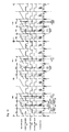
- FIG. 4 shows a timing chart showing a brief overview of the controller of the multi-phase electric motor according to the embodiment of the present invention. The details will be described in FIG. 5 and subsequent figures.
- the control period is 250 ⁇ sec, and the configuration thereof includes five periods of PWM signal based on the saw-tooth signal of 50 ⁇ sec period.
- the A/D conversion is performed aiming at the time of the timing in which the current value can be detected in the second and the third PWM period.
- the second PWM period is noted as a first detection period
- the third PWM period is noted as a second detection period.
- the detection is performed in the even number vector state (1, 1, 0) in the first detection period, and the detection is performed in the odd number vector state (1, 0, 0) in the second detection period, but either detection may be performed in either period, or both detections may be performed in the same period.
- the duties of the three phases are close to each other, where the duty is the maximum in the U phase, the intermediate in the V phase, and the minimum in the W phase.
- the U phase takes a high state
- the V phase takes a high state
- the W phase takes a low state
- the vector of the switching elements is (1, 1, 0).
- the number of switching elements to turn ON in the upper arm switching elements is an even number.
- the current value of the W phase should be detectable without shifting if the switching time interval between the V phase and the W phase is a sufficient length necessary for A/D conversion.
- the accurate current value of the W phase cannot be detected if the time interval between the V phase and the W phase is small.
- the U phase takes a high state
- the V phase takes a low state
- the W phase takes a low state
- the vector of the switching elements is (1, 0, 0).
- the number of switching elements to turn ON in the upper arm switching elements is an odd number.
- the current value of the U phase should be detectable without shifting if the switching time interval between the U phase and the V phase is a sufficient length necessary for A/D conversion.
- the accurate current value of the U phase cannot be detected if the time interval between the U phase and the V phase is small.
- the Duty maximum U phase is shifted to the right side (i.e., delay the phase) by the shift amount of MIN_DUTY (12%) - (maximum phase Duty% - intermediate phase Duty%) to ensure the phase difference 12% for detecting the accurate current value at the respective timing.
- the Duty minimum W phase is shifted to the left side (i.e., advance the phase) by the shift amount of MIN_DUTY (12%) - (intermediate phase Duty% - minimum phase Duty%).
- the broken line in the U phase and the W phase shows the PWM signal of each phase before shifting.
- the Duty intermediate V phase is not shifted. Similar shift process is performed in the five periods.
- the A/D conversion is performed at an optimum location of the detectable timing at when the current of two phases of the U phase, which is the Duty maximum phase, and the W phase, which is the Duty minimum phase, can be detected. That is, in the case of the current detection of the Duty minimum W phase, the period necessary for A/D conversion immediately before the fall of the PWM signal of the Duty intermediate V phase after the fall of the PWM signal of the W phase during the first detection period is the current detection period (shaded portion on the left side). In the case of the current detection of the Duty maximum U phase, the period necessary for A/D conversion immediately before the fall of the PWM signal of the U phase after the fall of the PWM signal of the V phase during the second detection period is the current detection period (shaded portion on the right side).
- FIG. 5 shows a timing chart in a case where the two phases are both detectable.
- the switching time interval between the V phase (duty 25%) and the W phase (50%) is sufficiently large.
- an accurate current value can be detected in such a time interval (vector in this case is (1, 0, 1)).
- the switching time interval between the U phase (75%) and the W phase (50%) is large.
- an accurate current value can also be detected in such a time interval (vector in this case is (1, 0, 0)). Therefore, shift does not need to be performed.
- the shunt resistor waveform in the figure represents the voltage waveform at both ends of the shunt resistor 26 (same below).
- the A/D conversion is performed at the optimum location of the detectable timing at when the current of two phases of the U phase, which is the Duty maximum phase, and the W phase, which is the Duty minimum phase, can be detected. That is, in the case of the current detection of the Duty minimum V phase, the A/D conversion is performed in a period necessary for A/D conversion immediately before the fall of the PWM signal of the W phase which is the Duty intermediate phase during the first detection period (shaded portion on the left side). In the case of the current detection of the Duty maximum U phase, the A/D conversion is performed in the period necessary for A/D conversion immediately before the fall of the PWM signal of the U phase during the second detection period (shaded portion on the right side).
- FIG. 6A shows a timing chart in a case where only the odd number vector is detectable.
- the switching time interval between the V phase (duty 39.6%) and the W phase (45.8%) is small. Thus, an accurate current value of the V phase cannot be detected in such a time interval.
- the switching time interval between the U phase (64.6%) and the W phase (45.8%) is large. Thus, an accurate current value of the U phase can be detected in such a time interval.
- the PWM signal of the V phase having the minimum duty of the three phases is phase shifted to the left side (to advance the phase) as shown in FIG. 6B since an accurate current value of the V phase cannot be detected in a state of even number vector, that is, in a state of (1, 0, 1) in this case.
- the switching time interval between the V phase and the W phase thereby becomes large.
- the accurate current value of the V phase then can be detected in the A/D converter since the current value stabilizes.
- the switching time interval between the U phase and the W phase is large even after the phase shift of the V phase.
- an accurate current value of the U phase can be detected in such a time interval.
- the A/D conversion is performed in a period necessary for A/D conversion immediately before the fall of the PWM signal of the W phase which is the Duty intermediate phase after the fall of the PWM signal of the V phase during the first detection period (shaded portion on the left side).
- the A/D conversion is performed in the period necessary for A/D conversion immediately before the fall of the PWM signal of the U phase after the fall of the PWM signal of the W phase during the second detection period (shaded portion on the right side).
- FIG. 7A shows a timing chart in a case where only the even number vector is detectable.
- the switching time interval between the V phase (duty 35.4%) and the W phase (54.2%) is large.
- an accurate current value of the V phase can be detected in such a time interval.
- the switching time interval between the U phase (60.4%) and the W phase (54.2%) is small.
- an accurate current value of the U phase cannot be detected in such a time interval.
- the PWM signal of the U phase having the maximum duty of the three phases is phase shifted to the right side (to delay the phase) as shown in FIG. 7B since an accurate current value of the U phase cannot be detected in a state of odd number vector, that is, in a state of (1, 0, 0) in this case.
- the switching time interval between the U phase and the W phase thereby becomes large.
- the accurate current value of the U phase then can be detected.
- the switching time interval between the V phase and the W phase is large even after the phase shift of the U phase.
- an accurate current value of the V phase can be detected in such a time interval.
- the A/D conversion is performed in a period necessary for A/D conversion immediately before the fall of the PWM signal of the W phase which is the Duty intermediate phase after the fall of the PWM signal of the V phase during the first detection period (shaded portion on the left side).
- the A/D conversion is performed in the period necessary for A/D conversion immediately before the fall of the PWM signal of the U phase after the fall of the PWM signal of the W phase during the second detection period (shaded portion on the right side).
- FIG. 8A shows a timing chart in a case where two phases are not detectable.
- the switching time interval between the V phase (duty 45%) and the W phase (50%) is small.
- an accurate current value of the V phase cannot be detected in such a time interval.
- the switching time interval between the U phase (55%) and the W phase (50%) is also small.
- an accurate current value of the U phase cannot be detected in such a time interval.
- the PWM signal of the V phase having the minimum duty is phase shifted to the left side (to advance the phase) as shown in FIG. 8B since an accurate current value of the V phase cannot be detected in the state of even number vector, that is, in a state of (1, 0, 1) in this case.
- the switching time interval between the V phase and the W phase thereby becomes large.
- the PWM signal of the U phase having the maximum duty is phase shifted to the right side (to delay the phase) as shown in FIG.
- the A/D conversion is performed in a period necessary for A/D conversion immediately before the fall of the PWM signal of the Duty intermediate W phase after the fall of the PWM signal of the V phase during the first detection period (shaded portion on the left side).
- the A/D conversion is performed in the period necessary for A/D conversion immediately before the fall of the PWM signal of the U phase after the fall of the PWM signal of the W phase during the second detection period (shaded portion on the right side).
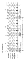
- FIG. 9 shows a timing chart in a case where two phases are not detectable in one control period.
- One control period is 250 ⁇ s, and includes five periods of the PWM signal based on the saw-tooth signal of 50 ⁇ sec period.
- the time interval between the V phase having duty minimum phase and the W phase having duty intermediate phase (vector in this case is (1, 0, 1)), and between the W phase of duty intermediate phase and the U phase having duty maximum phase (vector in this case is (1, 0, 0)) are both 5%, that is, short and thus the switching noise does not fall within the shunt waveform of the relevant period, and the A/D conversion time for accurately detecting the current value cannot be ensured.
- the PWM signal of the V phase having duty minimum phase is phase shifted to the left side (to advance phase), and the PWM signal of the U phase having the duty maximum phase is phase shifted to the right side (to delay the phase).
- the switching time intervals between the V phase and the W phase, and between the U phase and the W phase thus become large, and an accurate current value of the U phase and the V phase can be detected in the respective detection period.
- FIG. 10 shows a timing chart in a case where two phases in three control periods are not detectable.
- the shift of the PWM signal of the V phase and the U phase is performed in all five periods of each control period, and thus the period of the current ripple represented by the shunt waveform is 50 ⁇ sec, similar to the carrier period of the saw-tooth signal, and the frequency corresponding to such a period is not included in the audible range. Therefore, generation of noise can be prevented.
- a comparison regarding current ripple of the triangular signal and the saw-tooth signal is performed with respect to the carrier wave.
- the triangular signal has an advantage in that the current ripple is few compared to the saw-tooth signal. The reason is as described below.
- the PWM signal of one period is established from power running (when there is a difference in the ON/OFF state of each phase) and regeneration (when there is no difference in the ON/OFF state of each phase), but the current changes in the positive direction in power running.
- the current changes in the negative direction in regeneration.
- the slope of such change is determined by a time constant based on the inductance of the coil of the motor and the resistance of the coil of the motor.
- the current ripple generates when the state changes from power running to regeneration, or from regeneration to power running.
- the rise time of the PWM signal of each phase is the same in the saw-tooth signal.
- the state change of the power running and the regeneration in the saw-tooth signal of FIG. 11 is regeneration ⁇ power running ⁇ regeneration.
- the rise time of the PWM signal of each phase differs in the triangular signal.
- the state change of the power running and the regeneration in the triangular signal of FIG. 12 is regeneration ⁇ power running ⁇ regeneration ⁇ power running ⁇ regeneration.
- the number of changes of the current of one period is greater when using the triangular signal.
- the number of changes in one period is large. Therefore, the amount of change to positive/negative is small, and the current ripple becomes small.
- the number of changes in one period is small, and the amount of change to positive/negative is large. In other words, the current ripple is large.
- the phase shift is applied to one phase or two phases as in the present invention, a situation where the rise time of the PWM signal of each phase differs becomes greater even when the saw-tooth signal is used, and as a result, an advantage in that the current ripple becomes small is obtained.
- FIG. 13 shows a timing chart of the controller of the multi-phase electric motor when the saw-tooth signal is used.
- the time intervals between the V phase and the W phase (vector in this case is (1, 0, 1)), and between the W phase and the U phase (vector in this case is (1, 0, 0)) are 5%, that is, short, and thus the switching noise does not fall within the shunt waveform of the relevant period, and the A/D conversion time for accurately detecting the current value cannot be ensured.
- the Duty difference (12%) necessary for detection can be ensured by shifting the U phase having the maximum duty to the right side by 7% and the V phase having the minimum duty to the left side by 7%.
- FIG. 14 shows a timing chart of the controller of the multi-phase electric motor when the triangular signal is used. Similar to when the saw-tooth signal is used, a case where the U phase PWM signal is duty 55%, the V phase PWM signal is duty 45%, and the W phase PWM signal is duty 50% in the carrier period of 50 ⁇ sec is shown.
- the time intervals between the V phase and the W phase (vector in this case is (1, 0, 1)
- the W phase and the U phase vector in this case is (1, 0, 0)
- the time intervals between the V phase and the W phase are both 2.5%, that is, short since a phase difference is created on both sides.
- the carrier wave is the saw-tooth signal
- the length between the switching of the two phases is doubled compared to when the carrier wave is the triangular wave.
- an advantage is obtained in that there exist numerous three-phase PWM states in which the A/D conversion can be performed with the voltage waveform at both ends of the shunt resistor stabilized without performing the phase shift of the PWM signal.
- the A/D conversion is performed at optimum locations of the detectable timing at when the current of two phases, that is, the U phase, which is the Duty maximum phase, and the V phase, which is the Duty minimum phase, can be detected. For instance, when performing the A/D conversion in the second half of one period as in FIG. 14 , in the case of the current detection of the Duty minimum V phase, the A/D conversion is performed in the period necessary for A/D conversion immediately before the fall of the PWM signal of the Duty intermediate W phase during the first detection period (shaded portion on the left side).
- the A/D conversion is performed in the period necessary for A/D conversion immediately before the fall of the PWM signal of the U phase during the second detection period (shaded portion on the right side).
- the phase shift of each phase is performed through similar method when performing the A/D conversion in the first half of the one period, and the current can be detected in the A/D converter, and thus the description will not be given.
- the current value of each phase can be accurately detected for every control period using the single current detection means by shifting the PWM signal of each phase in the period of all five periods of each control period, and the frequency of the current ripple by switching based on the PWM signal is not included in the audible range, whereby the generation of noise can be prevented.
- the FET is used for the upper arm switching element and the lower arm switching element in the above embodiment, but other switching element such as IGBT (Insulated Gate Bipolar mode Transistor) may be used.
- the current detection means may adopt a configuration other than that shown in the embodiment, and may be arranged between the power supply and the FET bridge.
- a brushless motor is described in the above embodiment as a multi-phase electric motor by way of example, but the present invention can be applied to the general controller for controlling the electric motor including a plurality of phases such as induction motor and synchronous motor.
Landscapes
- Engineering & Computer Science (AREA)
- Power Engineering (AREA)
- Control Of Motors That Do Not Use Commutators (AREA)
- Control Of Ac Motors In General (AREA)
Applications Claiming Priority (1)
| Application Number | Priority Date | Filing Date | Title |
|---|---|---|---|
| JP2007304090A JP4884355B2 (ja) | 2007-11-26 | 2007-11-26 | 多相電動機の制御装置 |
Publications (3)
| Publication Number | Publication Date |
|---|---|
| EP2066021A2 true EP2066021A2 (de) | 2009-06-03 |
| EP2066021A3 EP2066021A3 (de) | 2014-03-26 |
| EP2066021B1 EP2066021B1 (de) | 2017-10-25 |
Family
ID=40210536
Family Applications (1)
| Application Number | Title | Priority Date | Filing Date |
|---|---|---|---|
| EP08169611.4A Ceased EP2066021B1 (de) | 2007-11-26 | 2008-11-21 | Steuervorrichtung von mehrphasigem Elektromotor |
Country Status (4)
| Country | Link |
|---|---|
| US (1) | US8203292B2 (de) |
| EP (1) | EP2066021B1 (de) |
| JP (1) | JP4884355B2 (de) |
| CN (1) | CN101499758B (de) |
Cited By (5)
| Publication number | Priority date | Publication date | Assignee | Title |
|---|---|---|---|---|
| US20110279076A1 (en) * | 2009-01-24 | 2011-11-17 | Markus Hirt | Electric motor, and device for generating a signal for controlling the same |
| JP2012065473A (ja) * | 2010-09-16 | 2012-03-29 | Ricoh Co Ltd | モータ駆動装置 |
| CN107819423A (zh) * | 2016-09-13 | 2018-03-20 | 福特全球技术公司 | 基于马达工作点的伪随机脉冲宽度调制变化 |
| EP3110001A4 (de) * | 2014-02-21 | 2018-03-28 | Mitsubishi Electric Corporation | Wechselstromdrehmaschinensteuerungsvorrichtung und steuerungsvorrichtung für eine elektrische servolenkung |
| CN110063017A (zh) * | 2016-11-25 | 2019-07-26 | 株式会社电装 | 马达控制装置以及马达驱动系统 |
Families Citing this family (29)
| Publication number | Priority date | Publication date | Assignee | Title |
|---|---|---|---|---|
| JP5252475B2 (ja) * | 2007-11-06 | 2013-07-31 | オムロンオートモーティブエレクトロニクス株式会社 | 多相電動機の制御装置 |
| JP4884356B2 (ja) * | 2007-11-26 | 2012-02-29 | オムロンオートモーティブエレクトロニクス株式会社 | 多相電動機の制御装置 |
| JP4650518B2 (ja) * | 2008-04-10 | 2011-03-16 | 株式会社デンソー | モータ制御装置 |
| JP2010221856A (ja) * | 2009-03-24 | 2010-10-07 | Hitachi Automotive Systems Ltd | 操舵制御装置 |
| TWI483552B (zh) * | 2009-07-20 | 2015-05-01 | Hon Hai Prec Ind Co Ltd | 脈衝寬度調變控制系統 |
| GB201004049D0 (en) * | 2010-03-11 | 2010-04-28 | Trw Ltd | Electric motor control |
| WO2012039094A1 (ja) * | 2010-09-24 | 2012-03-29 | 富士電機株式会社 | 電力変換装置およびその制御方法 |
| FR2969867B1 (fr) * | 2010-12-28 | 2015-03-20 | Renault Sa | Systeme de commande d'un ondulateur de tension alimentant un moteur electrique multiphase de vehicule automobile. |
| CN103534929B (zh) * | 2011-05-13 | 2017-03-29 | 株式会社日立制作所 | 同步电动机的驱动系统 |
| JP5344023B2 (ja) | 2011-11-21 | 2013-11-20 | 日本精工株式会社 | 電動パワーステアリング装置 |
| JP5557056B2 (ja) * | 2011-11-30 | 2014-07-23 | アイシン精機株式会社 | ポンプ制御ユニット |
| WO2013111968A1 (ko) * | 2012-01-25 | 2013-08-01 | Park In Gyu | 다상 전 브리지 전압원 인버터의 전류 제어 펄스 폭 변조 방법 |
| JP5641008B2 (ja) | 2012-04-04 | 2014-12-17 | 日本精工株式会社 | モータ制御装置及びそれを搭載した電動パワーステアリング装置 |
| JP5505449B2 (ja) * | 2012-04-06 | 2014-05-28 | 株式会社デンソー | 多相回転機の制御装置 |
| JP2014121896A (ja) * | 2012-12-20 | 2014-07-03 | Jtekt Corp | 電動パワーステアリング装置 |
| JP5908424B2 (ja) * | 2013-03-25 | 2016-04-26 | 日立オートモティブシステムズステアリング株式会社 | モータ制御装置およびパワーステアリング装置 |
| CN104871425B (zh) * | 2013-04-17 | 2017-07-11 | 日本精工株式会社 | 多相电动机控制装置及使用该多相电动机控制装置的电动助力转向装置 |
| JP2015050909A (ja) | 2013-09-04 | 2015-03-16 | オムロンオートモーティブエレクトロニクス株式会社 | モータ制御装置 |
| CN103929110B (zh) * | 2014-04-09 | 2017-09-15 | 东南大学 | 采用占空比直接求解脉宽调制的m相永磁电机控制方法 |
| JP6424500B2 (ja) * | 2014-07-11 | 2018-11-21 | 株式会社島津製作所 | 圧力制御装置および真空システム |
| EP3020615B1 (de) | 2014-09-17 | 2019-04-17 | NSK Ltd. | Elektrische servolenkvorrichtung |
| CN104953912B (zh) * | 2015-07-02 | 2017-06-27 | 武汉理工大学 | 基于矩阵变换器的电力推进船舶变频调速系统 |
| KR20170067934A (ko) * | 2015-12-08 | 2017-06-19 | 현대자동차주식회사 | 모터 제어 장치 |
| JP6583000B2 (ja) * | 2016-01-07 | 2019-10-02 | 株式会社デンソー | 回転電機の制御装置 |
| JP6529452B2 (ja) | 2016-03-11 | 2019-06-12 | 日立オートモティブシステムズ株式会社 | モータ駆動装置及びモータ駆動装置における相電流検出方法 |
| US10097115B2 (en) * | 2016-11-07 | 2018-10-09 | Infineon Technologies Ag | Auto-synchronization of brushless DC motors |
| CN107577217B (zh) * | 2017-08-23 | 2019-10-08 | 伊博电源(杭州)有限公司 | 一种交错并联控制逻辑电路及快速保护方法 |
| JP7407534B2 (ja) * | 2019-07-22 | 2024-01-04 | ミネベアミツミ株式会社 | モータ制御装置およびモータシステム |
| CN110798124A (zh) * | 2019-11-12 | 2020-02-14 | 广州视源电子科技股份有限公司 | Ipm过流保护方法与电路 |
Citations (8)
| Publication number | Priority date | Publication date | Assignee | Title |
|---|---|---|---|---|
| JPS6373898A (ja) | 1986-09-12 | 1988-04-04 | Matsushita Electric Ind Co Ltd | インバ−タ装置 |
| JP2540140B2 (ja) | 1987-01-13 | 1996-10-02 | オムロン株式会社 | 電動式パワ−ステアリングのモ−タ駆動装置 |
| JPH09191508A (ja) | 1995-12-29 | 1997-07-22 | Honda Motor Co Ltd | 電動車両の制御装置 |
| JPH10155278A (ja) | 1996-07-30 | 1998-06-09 | Texas Instr Inc <Ti> | インバータ制御方法および装置 |
| JP2001095279A (ja) | 1999-09-07 | 2001-04-06 | Trw Lucasvarity Electric Steering Ltd | モータ制御 |
| US6735537B2 (en) | 2002-03-15 | 2004-05-11 | Motorola, Inc. | Procedure for measuring the current in each phase of a three-phase device via single current sensor |
| JP2005531270A (ja) | 2002-06-07 | 2005-10-13 | ティーアールダブリュー・リミテッド | 空間ベクトル技法を使用する単一電流センサによるモータ駆動制御 |
| JP2007112416A (ja) | 2005-09-22 | 2007-05-10 | Jtekt Corp | 車両用操舵装置 |
Family Cites Families (18)
| Publication number | Priority date | Publication date | Assignee | Title |
|---|---|---|---|---|
| DE3486449T2 (de) * | 1983-11-28 | 1997-11-27 | Matsushita Electric Ind Co Ltd | Pulsbreitenmodulationswechselrichtervorrichtung |
| US6121736A (en) * | 1998-07-10 | 2000-09-19 | Matsushita Electric Industrial Co., Ltd. | Control apparatus for motor, and motor unit having the control apparatus |
| JP2002291284A (ja) * | 2001-03-26 | 2002-10-04 | Toshiba Kyaria Kk | 電動機の電流検出方法及び制御装置 |
| US6674258B2 (en) * | 2001-06-21 | 2004-01-06 | Matsushita Electric Industrial Co., Ltd. | Motor driver and motor drive method |
| JP2003047280A (ja) * | 2001-07-27 | 2003-02-14 | Mitsubishi Electric Corp | モータ駆動騒音低減装置およびモータ駆動騒音低減信号の作成方法 |
| JP4367130B2 (ja) * | 2001-09-29 | 2009-11-18 | ダイキン工業株式会社 | 相電流検出方法、インバータ制御方法、モータ制御方法およびこれらの装置 |
| JP3993502B2 (ja) * | 2002-10-21 | 2007-10-17 | 株式会社ルネサステクノロジ | 多相直流モータの回転駆動制御装置および起動方法 |
| JP3683259B2 (ja) * | 2003-06-03 | 2005-08-17 | 松下電器産業株式会社 | モータ駆動装置 |
| JP3951975B2 (ja) * | 2003-07-22 | 2007-08-01 | 株式会社日立製作所 | 交流電動機の制御装置,交流電動機の制御方法及びモジュール |
| JP4380247B2 (ja) * | 2003-08-25 | 2009-12-09 | アイシン・エィ・ダブリュ株式会社 | 電動駆動制御装置、電動駆動制御方法及びプログラム |
| US7049778B2 (en) * | 2004-02-09 | 2006-05-23 | Nippon Yusoki Co., Ltd. | Inverter control apparatus and inverter control method |
| JP2006025499A (ja) * | 2004-07-06 | 2006-01-26 | Favess Co Ltd | モータ制御装置 |
| WO2007049473A1 (ja) * | 2005-10-24 | 2007-05-03 | Matsushita Electric Industrial Co., Ltd. | インバータ装置 |
| US7193388B1 (en) * | 2006-02-02 | 2007-03-20 | Emerson Electric Co. | Offset PWM signals for multiphase motor |
| US7893638B2 (en) * | 2006-11-30 | 2011-02-22 | Denso Corporation | Apparatus and method for driving rotary machine |
| JP2008193825A (ja) * | 2007-02-06 | 2008-08-21 | Matsushita Electric Ind Co Ltd | Ad変換制御回路およびその関連技術 |
| JP5252475B2 (ja) * | 2007-11-06 | 2013-07-31 | オムロンオートモーティブエレクトロニクス株式会社 | 多相電動機の制御装置 |
| JP4884356B2 (ja) * | 2007-11-26 | 2012-02-29 | オムロンオートモーティブエレクトロニクス株式会社 | 多相電動機の制御装置 |
-
2007
- 2007-11-26 JP JP2007304090A patent/JP4884355B2/ja not_active Expired - Fee Related
-
2008
- 2008-11-13 CN CN200810174060XA patent/CN101499758B/zh not_active Expired - Fee Related
- 2008-11-21 EP EP08169611.4A patent/EP2066021B1/de not_active Ceased
- 2008-11-24 US US12/276,948 patent/US8203292B2/en not_active Expired - Fee Related
Patent Citations (8)
| Publication number | Priority date | Publication date | Assignee | Title |
|---|---|---|---|---|
| JPS6373898A (ja) | 1986-09-12 | 1988-04-04 | Matsushita Electric Ind Co Ltd | インバ−タ装置 |
| JP2540140B2 (ja) | 1987-01-13 | 1996-10-02 | オムロン株式会社 | 電動式パワ−ステアリングのモ−タ駆動装置 |
| JPH09191508A (ja) | 1995-12-29 | 1997-07-22 | Honda Motor Co Ltd | 電動車両の制御装置 |
| JPH10155278A (ja) | 1996-07-30 | 1998-06-09 | Texas Instr Inc <Ti> | インバータ制御方法および装置 |
| JP2001095279A (ja) | 1999-09-07 | 2001-04-06 | Trw Lucasvarity Electric Steering Ltd | モータ制御 |
| US6735537B2 (en) | 2002-03-15 | 2004-05-11 | Motorola, Inc. | Procedure for measuring the current in each phase of a three-phase device via single current sensor |
| JP2005531270A (ja) | 2002-06-07 | 2005-10-13 | ティーアールダブリュー・リミテッド | 空間ベクトル技法を使用する単一電流センサによるモータ駆動制御 |
| JP2007112416A (ja) | 2005-09-22 | 2007-05-10 | Jtekt Corp | 車両用操舵装置 |
Cited By (6)
| Publication number | Priority date | Publication date | Assignee | Title |
|---|---|---|---|---|
| US20110279076A1 (en) * | 2009-01-24 | 2011-11-17 | Markus Hirt | Electric motor, and device for generating a signal for controlling the same |
| US8686678B2 (en) * | 2009-01-24 | 2014-04-01 | Ebm-Papst St. Georgen Gmbh & Co. Kg | Electric motor, and device for generating a signal for controlling the same |
| JP2012065473A (ja) * | 2010-09-16 | 2012-03-29 | Ricoh Co Ltd | モータ駆動装置 |
| EP3110001A4 (de) * | 2014-02-21 | 2018-03-28 | Mitsubishi Electric Corporation | Wechselstromdrehmaschinensteuerungsvorrichtung und steuerungsvorrichtung für eine elektrische servolenkung |
| CN107819423A (zh) * | 2016-09-13 | 2018-03-20 | 福特全球技术公司 | 基于马达工作点的伪随机脉冲宽度调制变化 |
| CN110063017A (zh) * | 2016-11-25 | 2019-07-26 | 株式会社电装 | 马达控制装置以及马达驱动系统 |
Also Published As
| Publication number | Publication date |
|---|---|
| CN101499758B (zh) | 2012-06-27 |
| JP4884355B2 (ja) | 2012-02-29 |
| EP2066021A3 (de) | 2014-03-26 |
| EP2066021B1 (de) | 2017-10-25 |
| CN101499758A (zh) | 2009-08-05 |
| US8203292B2 (en) | 2012-06-19 |
| US20090146590A1 (en) | 2009-06-11 |
| JP2009131064A (ja) | 2009-06-11 |
Similar Documents
| Publication | Publication Date | Title |
|---|---|---|
| US8203292B2 (en) | Controller of multi-phase electric motor | |
| US8228012B2 (en) | Controller of multi-phase electric motor | |
| US7952310B2 (en) | Controller of multi-phase electric motor | |
| US5875414A (en) | Method and apparatus for protecting switching element of inverter from being overheated | |
| CN107148739B (zh) | 电力变换装置和应用该电力变换装置的车辆驱动系统 | |
| US8878477B2 (en) | Electric motor driving apparatus having failure detection circuit, and failure detection method for the electric motor driving apparatus having failure detection circuit | |
| KR101546605B1 (ko) | 모터 제어 장치 | |
| US10432124B2 (en) | Current detection apparatus and control apparatus of rotary electric machine | |
| CN103001568B (zh) | 马达控制装置 | |
| US10972026B2 (en) | Motor controlling device | |
| JP4833186B2 (ja) | 多相電動機の制御装置 | |
| JP4529113B2 (ja) | 電圧形インバータ及びその制御方法 | |
| JP2009124782A (ja) | 多相電動モータ制御装置 | |
| JP2009118681A (ja) | 多相電動機の制御装置 | |
| JP5252476B2 (ja) | 多相電動機の制御装置 | |
| WO2022130480A1 (ja) | 電力変換装置 | |
| KR100316638B1 (ko) | 데드-타임발생회로를없앤펄스폭변조인버터 | |
| JP4119996B2 (ja) | 交流電動機の駆動方法および駆動装置 |
Legal Events
| Date | Code | Title | Description |
|---|---|---|---|
| PUAI | Public reference made under article 153(3) epc to a published international application that has entered the european phase |
Free format text: ORIGINAL CODE: 0009012 |
|
| AK | Designated contracting states |
Kind code of ref document: A2 Designated state(s): AT BE BG CH CY CZ DE DK EE ES FI FR GB GR HR HU IE IS IT LI LT LU LV MC MT NL NO PL PT RO SE SI SK TR |
|
| AX | Request for extension of the european patent |
Extension state: AL BA MK RS |
|
| RAP1 | Party data changed (applicant data changed or rights of an application transferred) |
Owner name: OMRON AUTOMOTIVE ELECTRONICS CO., LTD. |
|
| PUAL | Search report despatched |
Free format text: ORIGINAL CODE: 0009013 |
|
| AK | Designated contracting states |
Kind code of ref document: A3 Designated state(s): AT BE BG CH CY CZ DE DK EE ES FI FR GB GR HR HU IE IS IT LI LT LU LV MC MT NL NO PL PT RO SE SI SK TR |
|
| AX | Request for extension of the european patent |
Extension state: AL BA MK RS |
|
| RIC1 | Information provided on ipc code assigned before grant |
Ipc: H02P 29/00 20060101AFI20140217BHEP Ipc: H02M 1/00 20070101ALI20140217BHEP Ipc: H02P 27/08 20060101ALI20140217BHEP Ipc: H02M 7/5395 20060101ALI20140217BHEP |
|
| 17P | Request for examination filed |
Effective date: 20140926 |
|
| RBV | Designated contracting states (corrected) |
Designated state(s): AT BE BG CH CY CZ DE DK EE ES FI FR GB GR HR HU IE IS IT LI LT LU LV MC MT NL NO PL PT RO SE SI SK TR |
|
| RIN1 | Information on inventor provided before grant (corrected) |
Inventor name: HAMASAKI, MASAMITSU |
|
| AKX | Designation fees paid |
Designated state(s): DE |
|
| RIC1 | Information provided on ipc code assigned before grant |
Ipc: H02M 7/5395 20060101ALI20160915BHEP Ipc: H02P 27/08 20060101ALI20160915BHEP Ipc: H02P 29/00 20160101AFI20160915BHEP Ipc: H02M 1/00 20060101ALI20160915BHEP |
|
| GRAP | Despatch of communication of intention to grant a patent |
Free format text: ORIGINAL CODE: EPIDOSNIGR1 |
|
| STAA | Information on the status of an ep patent application or granted ep patent |
Free format text: STATUS: GRANT OF PATENT IS INTENDED |
|
| INTG | Intention to grant announced |
Effective date: 20170509 |
|
| GRAS | Grant fee paid |
Free format text: ORIGINAL CODE: EPIDOSNIGR3 |
|
| GRAA | (expected) grant |
Free format text: ORIGINAL CODE: 0009210 |
|
| STAA | Information on the status of an ep patent application or granted ep patent |
Free format text: STATUS: THE PATENT HAS BEEN GRANTED |
|
| AK | Designated contracting states |
Kind code of ref document: B1 Designated state(s): DE |
|
| RIN1 | Information on inventor provided before grant (corrected) |
Inventor name: HAMASAKI, MASAMITSU |
|
| REG | Reference to a national code |
Ref country code: DE Ref legal event code: R096 Ref document number: 602008052619 Country of ref document: DE |
|
| REG | Reference to a national code |
Ref country code: DE Ref legal event code: R097 Ref document number: 602008052619 Country of ref document: DE |
|
| PLBE | No opposition filed within time limit |
Free format text: ORIGINAL CODE: 0009261 |
|
| STAA | Information on the status of an ep patent application or granted ep patent |
Free format text: STATUS: NO OPPOSITION FILED WITHIN TIME LIMIT |
|
| 26N | No opposition filed |
Effective date: 20180726 |
|
| PGFP | Annual fee paid to national office [announced via postgrant information from national office to epo] |
Ref country code: DE Payment date: 20220930 Year of fee payment: 15 |
|
| REG | Reference to a national code |
Ref country code: DE Ref legal event code: R119 Ref document number: 602008052619 Country of ref document: DE |
|
| PG25 | Lapsed in a contracting state [announced via postgrant information from national office to epo] |
Ref country code: DE Free format text: LAPSE BECAUSE OF NON-PAYMENT OF DUE FEES Effective date: 20240601 |
|
| PG25 | Lapsed in a contracting state [announced via postgrant information from national office to epo] |
Ref country code: DE Free format text: LAPSE BECAUSE OF NON-PAYMENT OF DUE FEES Effective date: 20240601 |