EP2066023A1 - Breitband-HF-Verstärker, der ein Verzerrungsreduzierungssystem umfasst und entspreches Verzerrungsreduzierungsverfahren - Google Patents
Breitband-HF-Verstärker, der ein Verzerrungsreduzierungssystem umfasst und entspreches Verzerrungsreduzierungsverfahren Download PDFInfo
- Publication number
- EP2066023A1 EP2066023A1 EP08168949A EP08168949A EP2066023A1 EP 2066023 A1 EP2066023 A1 EP 2066023A1 EP 08168949 A EP08168949 A EP 08168949A EP 08168949 A EP08168949 A EP 08168949A EP 2066023 A1 EP2066023 A1 EP 2066023A1
- Authority
- EP
- European Patent Office
- Prior art keywords
- amplifier
- signal
- pilot
- demodulator
- phase
- Prior art date
- Legal status (The legal status is an assumption and is not a legal conclusion. Google has not performed a legal analysis and makes no representation as to the accuracy of the status listed.)
- Granted
Links
- 238000000034 method Methods 0.000 title claims abstract description 15
- 230000003321 amplification Effects 0.000 claims description 15
- 238000003199 nucleic acid amplification method Methods 0.000 claims description 15
- 238000001514 detection method Methods 0.000 claims description 14
- 230000010363 phase shift Effects 0.000 claims description 14
- 238000012935 Averaging Methods 0.000 claims 1
- 101000843477 Escherichia coli (strain K12) RNA-binding protein Hfq Proteins 0.000 description 9
- 238000010586 diagram Methods 0.000 description 8
- 238000010719 annulation reaction Methods 0.000 description 6
- 239000003990 capacitor Substances 0.000 description 3
- 238000001228 spectrum Methods 0.000 description 3
- 241001644893 Entandrophragma utile Species 0.000 description 2
- 238000005516 engineering process Methods 0.000 description 2
- 238000001914 filtration Methods 0.000 description 2
- 230000003044 adaptive effect Effects 0.000 description 1
- 230000005540 biological transmission Effects 0.000 description 1
- 238000004891 communication Methods 0.000 description 1
- 230000000593 degrading effect Effects 0.000 description 1
- 239000000284 extract Substances 0.000 description 1
- 230000002452 interceptive effect Effects 0.000 description 1
Images




Classifications
-
- H—ELECTRICITY
- H03—ELECTRONIC CIRCUITRY
- H03F—AMPLIFIERS
- H03F1/00—Details of amplifiers with only discharge tubes, only semiconductor devices or only unspecified devices as amplifying elements
- H03F1/32—Modifications of amplifiers to reduce non-linear distortion
- H03F1/3223—Modifications of amplifiers to reduce non-linear distortion using feed-forward
- H03F1/3229—Modifications of amplifiers to reduce non-linear distortion using feed-forward using a loop for error extraction and another loop for error subtraction
- H03F1/3235—Modifications of amplifiers to reduce non-linear distortion using feed-forward using a loop for error extraction and another loop for error subtraction using a pilot signal
-
- H—ELECTRICITY
- H03—ELECTRONIC CIRCUITRY
- H03F—AMPLIFIERS
- H03F3/00—Amplifiers with only discharge tubes or only semiconductor devices as amplifying elements
- H03F3/189—High-frequency amplifiers, e.g. radio frequency amplifiers
- H03F3/19—High-frequency amplifiers, e.g. radio frequency amplifiers with semiconductor devices only
-
- H—ELECTRICITY
- H03—ELECTRONIC CIRCUITRY
- H03F—AMPLIFIERS
- H03F2200/00—Indexing scheme relating to amplifiers
- H03F2200/192—A hybrid coupler being used at the input of an amplifier circuit
-
- H—ELECTRICITY
- H03—ELECTRONIC CIRCUITRY
- H03F—AMPLIFIERS
- H03F2200/00—Indexing scheme relating to amplifiers
- H03F2200/204—A hybrid coupler being used at the output of an amplifier circuit
-
- H—ELECTRICITY
- H03—ELECTRONIC CIRCUITRY
- H03F—AMPLIFIERS
- H03F2200/00—Indexing scheme relating to amplifiers
- H03F2200/336—A I/Q, i.e. phase quadrature, modulator or demodulator being used in an amplifying circuit
-
- H—ELECTRICITY
- H03—ELECTRONIC CIRCUITRY
- H03F—AMPLIFIERS
- H03F2200/00—Indexing scheme relating to amplifiers
- H03F2200/451—Indexing scheme relating to amplifiers the amplifier being a radio frequency amplifier
-
- H—ELECTRICITY
- H03—ELECTRONIC CIRCUITRY
- H03F—AMPLIFIERS
- H03F2201/00—Indexing scheme relating to details of amplifiers with only discharge tubes, only semiconductor devices or only unspecified devices as amplifying elements covered by H03F1/00
- H03F2201/32—Indexing scheme relating to modifications of amplifiers to reduce non-linear distortion
- H03F2201/3212—Using a control circuit to adjust amplitude and phase of a signal in a signal path
Definitions
- the present invention relates to a broadband HF amplifier having an amplifier distortion reduction system over the entire amplification band and a distortion reduction method for such an amplifier. It is particularly applicable for broadband radio frequency power amplifiers operating in particular in the transmission bands of mobile telephone networks.
- RF power amplifiers which have to reconcile good electrical efficiency and good linearity over a wide band are generally made in class AB.
- the bandwidth of the signal is limited, for example of the order of 20 MHz for an amplifier operating in bands of the order of 1 to 10 GHz and when the non-linearity is simple, we prefer the method of pre-selection. distortion which is the least expensive.
- the principle of feedforward technology consists in extracting intermodulation products from the output signal of the power amplifier, or main amplifier and, after amplification by an error amplifier, to reinject these intermodulation products in phase opposition. with the output signal of the main amplifier.
- the feedforward amplifier 1 comprises a main amplifier 10 comprises a first signal cancellation loop 2 and an error amplifier 4 loops a loop of cancellation of the distortion on the output of the main amplifier.
- This adjustment must also be dynamic in real time to obtain good cancellation because a fine adjustment at the factory is not sufficient because of the variation of the characteristics of the amplifier in time and temperature in particular.
- the difficulty lies in the realization of an automatic control of the correction networks in amplitude and in phase and in particular in the realization of the automatic control of the correction networks of the second loop of the fact that in this last loop an important signal is superimposed on the distortion to be measured.
- the automatic control of the second loop is in particular traditionally based on the use of a pilot signal as described in particular in the document US 5,323,119 .
- the pilot signal may be a narrow band signal located outside the useful band, a narrowband signal scanned in the useful band as in the document US 5,307,022 or scanned in unoccupied parts of the useful band, two pilot signals located at each end of the useful band and slightly outside thereof and in particular, the document US 3,922,617 describes an adaptive feedforward system for an amplifier operating in class C and based on the use of two pilot signals.
- pilot signal consisting of two sidebands of a carrier located in the center of the useful band so as to frame the useful signal or use a broadband signal located in the useful band.
- the general principle is to detect the residual pilot, after cancellation in the second loop, thanks to the reference signal coming from the pilot signal generator.
- a quadrature demodulator extracts the I and Q components of the residual driver.
- the voltages corresponding to the I and Q components are applied to the amplitude and phase adjustment networks.
- the phase of the reference signal is adjusted so that the control loop is a negative feedback loop on both I and Q components.
- the difficulty is to detect the residual driver which is very small in amplitude in the presence of a broadband signal whose amplitude is typically 60 dB higher than that of the residual pilot.
- the figure 4 schematizes a device of the prior art single pilot located outside the useful band and the figure 5 a typical cancellation curve when using a driver located below the useful band.
- the correction networks 5, 6 of the distortion cancellation loop 3 are controlled by an I / Q demodulator receiving a reference reference signal ref phase-shifted by a network 10 and the residual pilot at the output of the amplifier.
- the pilot is often placed just below the useful band so that the residual pilot is weak enough not to disturb the system.
- the fact that it is outside the useful band makes it possible to increase slightly its level insofar as it can be filtered at the exit of the system.
- the demodulator can be protected by a filter that will attenuate the system signal while allowing the residual driver to pass and the demodulator dynamics can be increased.
- the example of figure 6 represents the cancellation curve A obtained in the case of a device using a spread spectrum driver 12.
- the spread spectrum technique makes it possible to keep a pilot at a global level of power sufficient to perform detection while keeping a very low pilot level at each frequency point.
- the disadvantage of this solution is that the dynamic stress on the demodulator is important and that no prior filtering can be performed.
- the detection of the modulation makes it possible to adjust the phase grating and the amplitude network of the second loop.
- the signals are two separate pilot signals and arranged at each end of the useful band, it is then possible to adjust an amplitude network and a phase grating with flat frequency responses using the first pilot and an amplitude network and a phase grating whose frequency responses have a slope using the second pilot.
- the error correction device comprises a single phase correction means and a single amplitude correction means, in a distortion cancellation loop of the amplifier.
- the error correction device comprises switching means adapted to inject alternately the two pilot signals input to the amplifier and adapted to generate a switching signal for alternately controlling a corresponding demodulation stage.
- switching means adapted to inject alternately the two pilot signals input to the amplifier and adapted to generate a switching signal for alternately controlling a corresponding demodulation stage.
- BF controlling said phase and amplitude correction networks.
- the HF detection is preferably carried out using a single HF demodulator, of the HF I / Q demodulator type according to the example, simultaneously receiving on its first input the first and second reference pilot signals. and on its second input the output signal of the amplifier through a filter adapted to pass the residual pilot signals and attenuate the frequencies in the band of the amplifier.
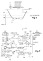
- the invention provides a broadband HF amplifier 100 having an amplifier distortion reduction system over the entire feedforward correction amplification band shown globally in FIG. figure 7 .
- the amplifier comprises an amplification module 123 disposed in a known manner in a first compensation loop 122 comprising phase correction and amplitude correction networks 120, 121 of the first loop which is not the object of the present invention. request.
- a second control loop is necessary and the present invention, which relates to this second loop uses a first pilot signal P1 and a second pilot signal P2 and a cancellation loop 103 comprising an error correction device based on the two pilot signals.
- the error correction device comprises first means 104 for adjusting a phase difference close to 0 ° (possibly modulo 360 °) between the first pilot signal and the residual signal of this first pilot signal.
- the introduced phase difference does not need, in the case of the present invention, to be of a very high precision and an error of + or - 10 ° is tolerable without degrading very significantly the cancellation of the distortion which remains even in this case lower than the value of -30dB that one seeks to obtain.
- the first phase difference adjusting means 104 comprise a first phase-shifting means arranged between a generator 101 of the first pilot signal P1 and a first input 107 of an HF demodulator 106 receiving on a second input 108 the residual signal P1r derived from of the first pilot signal at the output of the RF amplifier, the first phase-shifting means providing a first phase shift reference signal refP1 whose phase-shift compensates the phase difference from the input of the amplifier to the second input of the demodulator 106 and introducing an additional phase shift so that the 2 signals refP1 and P1r are in phase.
- the second means 105 for adjusting a phase difference for their part comprise a second phase-shifting means arranged between a generator 102 of the second pilot signal and a first input 107 of an HF demodulator 106 receiving on a second input 108 the residual signal P2r from the second pilot signal at the output of the RF amplifier, the phase shifter means 105 providing a second phase shifted reference signal refP2 whose phase shift compensates the phase shift from the input of the amplifier to the second input of the demodulator 106 and introducing a further phase shift of the order of 180 ° so that the two signals are in phase opposition.
- the cancellation loop 103 of the amplifier comprises a single phase correction means 111 and a single amplitude correction means 112. These means are according to the invention.
- the example constituted by a phase correction network and an amplitude correction network but can be equivalently grouped into a single I / Q modulation network producing a phase correction means and an amplitude correction means .
- the broadband HF amplifier of the invention advantageously comprises switching means 113, 113a adapted to alternately inject the two pilot signals at the input of the amplifier and adapted to generate a switching signal d for alternately controlling a stage of correspondence.
- demodulating BF 114 controlling said phase and amplitude correction networks 111, 112 of the cancellation loop 103.
- the HF detection is carried out using a single HF demodulator 106, which according to the example is HF I / Q demodulator type.
- the first and second reference pilot signals refP1, refP2, one of which is out of phase, are received on the first input 107 of the HF I / Q demodulator 106, input LO on the figure 8 , and the output signal of the amplifier is received on the second input of the RF I / Q demodulator, RF input on the figure 8 through a filter 115 shown in FIG. figure 7 and adapted to pass the residual pilot signals P1r, P2r and attenuate the frequencies S located in the band of the amplifier.
- This cut-off type filter 115 attenuates the amplified signals S by the amplifier in the useful band to improve the detection of the residual pilot signals P1r, P2r which are injected at a level close to the level of the distortion of the amplifier. .
- the residual drivers P1r and P2r are received alternately on the RF input of the RF mixer.
- the invention makes it possible to use only one receiver device consisting of the HF demodulator 106, the BF demodulator 114 and the phase and amplitude correction networks 111 112 while employing two pilot signals which does not make the system much more complicated than a single pilot system and much less complicated than a complete two-pilot system and for which all the detection and correction means are duplicated.
- the invention makes it possible to use two drivers located at each end of the band of the amplifier but to use only one detector and to average the detection information of the two pilots so as to regulate only a single amplitude network and a single phase network.
- the residual error on each network is reduced by a factor of 2 by distributing it between the base of the band and the top of the band.
- Adjusting the 180 ° phase difference on the refP1 and refP2 channels allows the drivers to be used in a Push-Pull configuration.
- the cancellation loop comprises a direct channel passing through the delay network 202 and a cancellation path passing through the phase correction means 111, the amplitude correction means 112 and an error amplifier 201. two paths meet at the coupler 203.
- the direct channel passes the direct signal Sd superimposed on the signal S that it is desired to amplify, and in the cancellation channel passes the error signal Se.
- the signals Sd and Se are of equal amplitude and in phase opposition so that they cancel at the coupler 203.
- the amplitude information is found on the detection output I, and the phase information is found on the detection output Q. This allows to attack indifferently amplitude modulation networks or I / Q for small variations ⁇ A and ⁇ around the perfect cancellation.
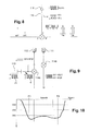
- the signals present on the mixer or HF demodulator 106 are represented more precisely in FIG. figure 12 for processing the signal refP1 and the resulting error signal P1r at a time n when the demodulator receives on its input 108 RF the signal P1r taken at the amplification output and, at the figure 13 at time n + 1 when the demodulator receives on its input 108 the signal P2r.
- the RF demodulator receives on its first input 107, input LO, the two signals refP1 and refP2 combined, comprises after its first input a 90 ° divider 124 for driving first inputs of two FET mixers or Schottky diode mixers 106a, 106b.
- the RF demodulator alternately receives on its second input 108, input R, the remaining pilots P1r, P2r.
- the first mixer 106a receiving the signals without phase shift provides on the output 116 the component of the error on the axis I direct axis of the complex plane and the second mixer 106b which receives the signals with phase shift of 90 ° provides on its output 117 the component of the error on the axis Q of the complex plane axis at 90 ° of the axis I.
- the arrows represent the directions of the components and in this case the components give positive voltages for the error components on P1, the signal P1r being in the first quadrant I / Q.
- the output voltage is then + ⁇ Va1, which is the sum of the offset and the error voltage due to the real part of P1r on the output 116, output 1, and + ⁇ Vph1, voltage which is the sum of the offset and the error voltage due to the imaginary part of P1r or the phase shift of P1r on the output 117, output Q.
- the arrows represent the directions of the components and in this case, the components give at the output negative voltages for the error components on P2.
- the output voltage is then + ⁇ Va2, which is the sum of the offset and the negative error voltage due to the real part of P2r on the output 116, output I, and + ⁇ Vph2, which is the sum the offset and the negative error voltage due to the phase shift of P2r on the output 117, output Q.
- a four-quadrant multiplier-type demodulation stage BF 114 is used, for example those known under the references MC 1496 or SA612 represented diagrammatically in FIG. figure 9 and which comprises two BF mixers 114a, 114b, one receiving on a first channel a signal coming from the output I 116 of said I / Q HF demodulator, the other receiving on a first channel a signal coming from the Q output 117 of said I / Q HF demodulator, the two BF mixers 114a, 114b receiving on their second channels the d switching signal generated by the switching means 113 of the figure 7 .
- the figure 14 represents an example of a link between an output channel of the I / Q type RF demodulator and a demodulation channel BF.
- an error signal is obtained comprising an offset component (DC offset) due to the demodulator and an alternating component around the offset voltage whose peak-to-peak value corresponds to the sum of the errors ⁇ V1, ⁇ V2 on the two drivers P1, P2.
- the device includes signal amplification means 118 and DC component canceling means 119 between the I / Q RF demodulator and the RF mixers. These means are provided to suppress the offset voltage of the HF I / Q demodulator. To do this, a first capacitor 119 is arranged in series between the output 116 and an amplification stage of the error signal 118 and a second capacitor 119 is arranged between the amplification stage 118 and the first input 128 of the mixer BF. 114a.
- the second input of the mixer 114a receives the switching signal d generated by the switching means 113 of the figure 7 possibly recentered around a zero voltage by a capacitor 129.
- the principle is that the peak-to-peak value signal ⁇ V1 + ⁇ V2 is multiplied by the switching signal to obtain a signal equal to the average of the deviations.
- the mixers BF are thus adapted to rectify the error signals from the I / Q demodulator HF to provide a voltage by means of errors on the two pilot signals P1 and P2.
- the cancellation loop will then continuously seek to minimize the sum of the residual drivers ⁇ V1 + ⁇ V2 for each of the I and Q controls, which optimizes the cancellation for the entire band from P1 to P2 and the cancellation to the
- the use of the two push-pull pilots of the invention is comparable to a pilot-pilot system or two-pilot system and two prior art detections for a greatly reduced complexity.
- the clipping signal d is a pseudo-random sequence whose probability of occurrence of the states highs and lows is identical.
- one of the first or second pilot signals P1, P2 is generated at a frequency lower than or equal to the low frequency of the amplifier band, the other of first and second pilot signals P1, P2 being generated at a frequency greater than or equal to the high frequency of said band.
- the invention is applicable to broadband amplifiers for example operating for the GSM, DCS and UMTS bands and in the bands of the future standard 4G, ie bands whose width can be up to 100 MHz.
- the distortion reduction system of the invention thus makes it possible, with the aid of two pilots, a single amplitude correction network and a single phase correction network, to reduce the maximum residual error by a factor of 2 on each network by distributing it at the top and bottom of the amplifier band.
- a phase difference close to 0 ° is adjusted between the first pilot signal and the residual signal of this first pilot signal at the output of the amplifier for providing a reference signal refP1
- a phase difference close to 180 ° is adjusted between the second pilot signal and the residual signal of this second signal.
- the two pilot signals are alternately injected at the input of the amplifier and a switching signal d is generated to alternately control a BF 114 demodulation stage controlling phase correction networks and of amplitude 111, 112 of the cancellation loop 103.
- the BF demodulation stage 114 comprising two BF mixers 114a, 114b, one receiving on a first channel a signal coming from the I 116 output I / Q HF demodulator, the other receiving on a first channel a signal from the Q output 117 of said I / Q HF demodulator, is injected on the second channel BF mixers 114a, 114b the d clipping signal to average the amplitudes error correction signals.
- the single amplitude correction network and the single phase correction network are then driven using the output signals of the RF mixers.
- the first and second reference pilot signals refP1, refP2 are injected on its first input 107 and on its second input on amplifier output signal through a filter 115 adapted to pass the residual pilot signals P1r, P2r and attenuate the S frequencies in the band of the amplifier.
- one of the first or second pilot signals P1, P2 is generated at a frequency lower than or equal to the low frequency of the amplifier band and the other of the first and second frequencies is generated.
- second pilot signals P1, P2 at a frequency greater than or equal to the high frequency of said band.
Landscapes
- Engineering & Computer Science (AREA)
- Power Engineering (AREA)
- Physics & Mathematics (AREA)
- Nonlinear Science (AREA)
- Amplifiers (AREA)
- Magnetic Resonance Imaging Apparatus (AREA)
Applications Claiming Priority (1)
| Application Number | Priority Date | Filing Date | Title |
|---|---|---|---|
| FR0759422A FR2924542B1 (fr) | 2007-11-29 | 2007-11-29 | Amplificateur hf large bande comportant un systeme de reduction de distorsion et procede de reduction de distorsion associe |
Publications (2)
| Publication Number | Publication Date |
|---|---|
| EP2066023A1 true EP2066023A1 (de) | 2009-06-03 |
| EP2066023B1 EP2066023B1 (de) | 2011-06-29 |
Family
ID=39247789
Family Applications (1)
| Application Number | Title | Priority Date | Filing Date |
|---|---|---|---|
| EP08168949A Not-in-force EP2066023B1 (de) | 2007-11-29 | 2008-11-12 | Breitband-HF-Verstärker, der ein Verzerrungsreduzierungssystem umfasst und entspreches Verzerrungsreduzierungsverfahren |
Country Status (3)
| Country | Link |
|---|---|
| EP (1) | EP2066023B1 (de) |
| AT (1) | ATE515106T1 (de) |
| FR (1) | FR2924542B1 (de) |
Citations (8)
| Publication number | Priority date | Publication date | Assignee | Title |
|---|---|---|---|---|
| US3922617A (en) | 1974-11-18 | 1975-11-25 | Cutler Hammer Inc | Adaptive feed forward system |
| US5307022A (en) | 1991-04-15 | 1994-04-26 | Motorola, Inc. | High dynamic range modulation independent feed forward amplifier network |
| US5323119A (en) | 1989-11-16 | 1994-06-21 | Motorola, Inc. | Amplifier having feed forward cancellation |
| US5493252A (en) * | 1993-11-24 | 1996-02-20 | Nec Corporation | Feedforward distortion compensation circuit |
| EP0991210A2 (de) * | 1998-09-29 | 2000-04-05 | Lucent Technologies Inc. | Doppelseitenbandpilottechnik eines Kontrollsystems für Reduktion die durch die elektrische Schaltung generierte Verzerrung |
| EP1267486A2 (de) * | 2001-06-11 | 2002-12-18 | Matsushita Electric Industrial Co., Ltd. | Regelverfahren und Regelschaltung für einen vorwärtsgekoppelten verzerrungskompensierten Verstärker |
| JP2003142948A (ja) * | 2001-11-06 | 2003-05-16 | Japan Radio Co Ltd | フィードフォワード増幅器及びその制御回路 |
| WO2005091802A2 (en) | 2004-03-11 | 2005-10-06 | Powerwave Technologies, Inc. | System and method for control of loop alignment in adaptive feed forward amplifiers |
-
2007
- 2007-11-29 FR FR0759422A patent/FR2924542B1/fr not_active Expired - Fee Related
-
2008
- 2008-11-12 EP EP08168949A patent/EP2066023B1/de not_active Not-in-force
- 2008-11-12 AT AT08168949T patent/ATE515106T1/de not_active IP Right Cessation
Patent Citations (9)
| Publication number | Priority date | Publication date | Assignee | Title |
|---|---|---|---|---|
| US3922617A (en) | 1974-11-18 | 1975-11-25 | Cutler Hammer Inc | Adaptive feed forward system |
| US5323119A (en) | 1989-11-16 | 1994-06-21 | Motorola, Inc. | Amplifier having feed forward cancellation |
| US5307022A (en) | 1991-04-15 | 1994-04-26 | Motorola, Inc. | High dynamic range modulation independent feed forward amplifier network |
| US5493252A (en) * | 1993-11-24 | 1996-02-20 | Nec Corporation | Feedforward distortion compensation circuit |
| EP0991210A2 (de) * | 1998-09-29 | 2000-04-05 | Lucent Technologies Inc. | Doppelseitenbandpilottechnik eines Kontrollsystems für Reduktion die durch die elektrische Schaltung generierte Verzerrung |
| US6157254A (en) | 1998-09-29 | 2000-12-05 | Lucent Technologies Inc. | Double side band pilot technique for a control system that reduces distortion produced by electrical circuits |
| EP1267486A2 (de) * | 2001-06-11 | 2002-12-18 | Matsushita Electric Industrial Co., Ltd. | Regelverfahren und Regelschaltung für einen vorwärtsgekoppelten verzerrungskompensierten Verstärker |
| JP2003142948A (ja) * | 2001-11-06 | 2003-05-16 | Japan Radio Co Ltd | フィードフォワード増幅器及びその制御回路 |
| WO2005091802A2 (en) | 2004-03-11 | 2005-10-06 | Powerwave Technologies, Inc. | System and method for control of loop alignment in adaptive feed forward amplifiers |
Also Published As
| Publication number | Publication date |
|---|---|
| FR2924542A1 (fr) | 2009-06-05 |
| FR2924542B1 (fr) | 2010-01-01 |
| ATE515106T1 (de) | 2011-07-15 |
| EP2066023B1 (de) | 2011-06-29 |
Similar Documents
| Publication | Publication Date | Title |
|---|---|---|
| EP0773654A1 (de) | Direktdemodulationsstufe für quadraturmodulierte Signale, und Empfänger damit | |
| FR2924540A1 (fr) | Systemes, procedes et appareils de predistorsion recursive orthogonale par trajets multiples | |
| EP3785367B1 (de) | System und verfahren zur basisbandlinearisierung für einen hochfrequenzleistungsverstärker der klasse g | |
| EP1269707B1 (de) | Vorrichtung zur erzeugung eines phasen- und amplitudenmodulierten hochfrequenzsignals | |
| FR2835120A1 (fr) | Procede et dispositif de preparation de signaux destines a etre compares pour etablir une pre-distorsion sur l'entree d'un amplificateur | |
| FR2716589A1 (fr) | Amplificateur de puissance à commande de modulation d'amplitude et commande de modulation de phase imbriquées. | |
| WO2014113246A1 (en) | Generation of an optical local-oscillator signal for a coherent-detection scheme | |
| WO2014113275A1 (en) | Optical polarization demultiplexing for a coherent-detection scheme | |
| CN103430003B (zh) | 用于估计接收到的光信号的色散的方法 | |
| CA2446541A1 (fr) | Pre-distortion adaptative d'un generateur d'un signal radiofrequence module en phase ou frequence et en amplitude | |
| WO2002101916A2 (fr) | Procede de modulation de l'amplitude d'un signal radiofrequence, et dispositif pour sa mise en oeuvre | |
| CA2027890C (fr) | Procede de correction numerique de non linearite d'une chaine d'emission, et dispositif de mise en oeuvre de ce procede | |
| FR2991527A1 (fr) | Procede de calibration de lineariseur et composant electronique linearise | |
| WO2007101885A1 (fr) | Dispositif de recepion et/ou d'emission de signaux radiofrequences a reduction du bruit | |
| EP0113611A1 (de) | Einrichtung zur automatischen Linearisierung der Frequenz-Steuersignal-Charakteristik eines in Frequenz modulierten Oszillators mit variabler Frequenz | |
| EP0775390B1 (de) | Gerät zum korrigieren der amplituden-/frequenzcharakteristik eines ein kabel durchlaufenden signals und entsprechender frequenzentzerrer | |
| FR2669165A1 (fr) | Appareil et procede permettant de faire varier un signal dans l'emetteur d'un emetteur-recepteur. | |
| EP2066023B1 (de) | Breitband-HF-Verstärker, der ein Verzerrungsreduzierungssystem umfasst und entspreches Verzerrungsreduzierungsverfahren | |
| FR2517141A1 (fr) | Procede et dispositif de commande automatique de gain pour une transmission en modulation de frequence | |
| EP0081413B1 (de) | Retransmissionseinrichtung mit gemeinsamer Bild-/Tonträgerverstärkung und automatischer Steuerung des Bild-/Tonverhältnisses | |
| EP0141715B1 (de) | Vorrichtung zur automatischen Vorkorrektur von Nichtlinearitäten in einer Leistungsverstärkerkette, sowie ihre Anwendung in einem Fernsehsender | |
| WO2011000882A1 (fr) | Generateur d'un signal radiofrequence module, procede de calibration du generateur et systeme d'imagerie par resonance magnetique | |
| CA2312834A1 (en) | Carrier reutilization for synchronous detection | |
| FR2541058A1 (fr) | Dispositif de linearisation d'amplificateur haute frequence a coefficients de non-linearite complexes | |
| EP2533428A1 (de) | Drahtloses Multistandardsender |
Legal Events
| Date | Code | Title | Description |
|---|---|---|---|
| PUAI | Public reference made under article 153(3) epc to a published international application that has entered the european phase |
Free format text: ORIGINAL CODE: 0009012 |
|
| AK | Designated contracting states |
Kind code of ref document: A1 Designated state(s): AT BE BG CH CY CZ DE DK EE ES FI FR GB GR HR HU IE IS IT LI LT LU LV MC MT NL NO PL PT RO SE SI SK TR |
|
| AX | Request for extension of the european patent |
Extension state: AL BA MK RS |
|
| 17P | Request for examination filed |
Effective date: 20091202 |
|
| AKX | Designation fees paid |
Designated state(s): AT BE BG CH CY CZ DE DK EE ES FI FR GB GR HR HU IE IS IT LI LT LU LV MC MT NL NO PL PT RO SE SI SK TR |
|
| GRAP | Despatch of communication of intention to grant a patent |
Free format text: ORIGINAL CODE: EPIDOSNIGR1 |
|
| GRAC | Information related to communication of intention to grant a patent modified |
Free format text: ORIGINAL CODE: EPIDOSCIGR1 |
|
| GRAS | Grant fee paid |
Free format text: ORIGINAL CODE: EPIDOSNIGR3 |
|
| GRAA | (expected) grant |
Free format text: ORIGINAL CODE: 0009210 |
|
| RIN1 | Information on inventor provided before grant (corrected) |
Inventor name: GUILLEMET, OLIVIER Inventor name: POWELL, .JACK |
|
| AK | Designated contracting states |
Kind code of ref document: B1 Designated state(s): AT BE BG CH CY CZ DE DK EE ES FI FR GB GR HR HU IE IS IT LI LT LU LV MC MT NL NO PL PT RO SE SI SK TR |
|
| REG | Reference to a national code |
Ref country code: GB Ref legal event code: FG4D Free format text: NOT ENGLISH |
|
| REG | Reference to a national code |
Ref country code: CH Ref legal event code: EP |
|
| REG | Reference to a national code |
Ref country code: IE Ref legal event code: FG4D Free format text: LANGUAGE OF EP DOCUMENT: FRENCH |
|
| REG | Reference to a national code |
Ref country code: DE Ref legal event code: R096 Ref document number: 602008007917 Country of ref document: DE Effective date: 20110818 |
|
| REG | Reference to a national code |
Ref country code: NL Ref legal event code: VDEP Effective date: 20110629 |
|
| REG | Reference to a national code |
Ref country code: SE Ref legal event code: TRGR |
|
| PG25 | Lapsed in a contracting state [announced via postgrant information from national office to epo] |
Ref country code: HR Free format text: LAPSE BECAUSE OF FAILURE TO SUBMIT A TRANSLATION OF THE DESCRIPTION OR TO PAY THE FEE WITHIN THE PRESCRIBED TIME-LIMIT Effective date: 20110629 Ref country code: NO Free format text: LAPSE BECAUSE OF FAILURE TO SUBMIT A TRANSLATION OF THE DESCRIPTION OR TO PAY THE FEE WITHIN THE PRESCRIBED TIME-LIMIT Effective date: 20110929 Ref country code: LT Free format text: LAPSE BECAUSE OF FAILURE TO SUBMIT A TRANSLATION OF THE DESCRIPTION OR TO PAY THE FEE WITHIN THE PRESCRIBED TIME-LIMIT Effective date: 20110629 |
|
| PG25 | Lapsed in a contracting state [announced via postgrant information from national office to epo] |
Ref country code: SI Free format text: LAPSE BECAUSE OF FAILURE TO SUBMIT A TRANSLATION OF THE DESCRIPTION OR TO PAY THE FEE WITHIN THE PRESCRIBED TIME-LIMIT Effective date: 20110629 Ref country code: FI Free format text: LAPSE BECAUSE OF FAILURE TO SUBMIT A TRANSLATION OF THE DESCRIPTION OR TO PAY THE FEE WITHIN THE PRESCRIBED TIME-LIMIT Effective date: 20110629 Ref country code: LV Free format text: LAPSE BECAUSE OF FAILURE TO SUBMIT A TRANSLATION OF THE DESCRIPTION OR TO PAY THE FEE WITHIN THE PRESCRIBED TIME-LIMIT Effective date: 20110629 Ref country code: GR Free format text: LAPSE BECAUSE OF FAILURE TO SUBMIT A TRANSLATION OF THE DESCRIPTION OR TO PAY THE FEE WITHIN THE PRESCRIBED TIME-LIMIT Effective date: 20110930 Ref country code: AT Free format text: LAPSE BECAUSE OF FAILURE TO SUBMIT A TRANSLATION OF THE DESCRIPTION OR TO PAY THE FEE WITHIN THE PRESCRIBED TIME-LIMIT Effective date: 20110629 |
|
| REG | Reference to a national code |
Ref country code: IE Ref legal event code: FD4D |
|
| PG25 | Lapsed in a contracting state [announced via postgrant information from national office to epo] |
Ref country code: CZ Free format text: LAPSE BECAUSE OF FAILURE TO SUBMIT A TRANSLATION OF THE DESCRIPTION OR TO PAY THE FEE WITHIN THE PRESCRIBED TIME-LIMIT Effective date: 20110629 Ref country code: IE Free format text: LAPSE BECAUSE OF FAILURE TO SUBMIT A TRANSLATION OF THE DESCRIPTION OR TO PAY THE FEE WITHIN THE PRESCRIBED TIME-LIMIT Effective date: 20110629 Ref country code: IS Free format text: LAPSE BECAUSE OF FAILURE TO SUBMIT A TRANSLATION OF THE DESCRIPTION OR TO PAY THE FEE WITHIN THE PRESCRIBED TIME-LIMIT Effective date: 20111029 Ref country code: EE Free format text: LAPSE BECAUSE OF FAILURE TO SUBMIT A TRANSLATION OF THE DESCRIPTION OR TO PAY THE FEE WITHIN THE PRESCRIBED TIME-LIMIT Effective date: 20110629 Ref country code: NL Free format text: LAPSE BECAUSE OF FAILURE TO SUBMIT A TRANSLATION OF THE DESCRIPTION OR TO PAY THE FEE WITHIN THE PRESCRIBED TIME-LIMIT Effective date: 20110629 Ref country code: PT Free format text: LAPSE BECAUSE OF FAILURE TO SUBMIT A TRANSLATION OF THE DESCRIPTION OR TO PAY THE FEE WITHIN THE PRESCRIBED TIME-LIMIT Effective date: 20111031 |
|
| PG25 | Lapsed in a contracting state [announced via postgrant information from national office to epo] |
Ref country code: PL Free format text: LAPSE BECAUSE OF FAILURE TO SUBMIT A TRANSLATION OF THE DESCRIPTION OR TO PAY THE FEE WITHIN THE PRESCRIBED TIME-LIMIT Effective date: 20110629 Ref country code: CY Free format text: LAPSE BECAUSE OF FAILURE TO SUBMIT A TRANSLATION OF THE DESCRIPTION OR TO PAY THE FEE WITHIN THE PRESCRIBED TIME-LIMIT Effective date: 20110629 Ref country code: RO Free format text: LAPSE BECAUSE OF FAILURE TO SUBMIT A TRANSLATION OF THE DESCRIPTION OR TO PAY THE FEE WITHIN THE PRESCRIBED TIME-LIMIT Effective date: 20110629 Ref country code: SK Free format text: LAPSE BECAUSE OF FAILURE TO SUBMIT A TRANSLATION OF THE DESCRIPTION OR TO PAY THE FEE WITHIN THE PRESCRIBED TIME-LIMIT Effective date: 20110629 |
|
| PLBE | No opposition filed within time limit |
Free format text: ORIGINAL CODE: 0009261 |
|
| STAA | Information on the status of an ep patent application or granted ep patent |
Free format text: STATUS: NO OPPOSITION FILED WITHIN TIME LIMIT |
|
| BERE | Be: lapsed |
Owner name: LPA CONCEPTS Effective date: 20111130 |
|
| PG25 | Lapsed in a contracting state [announced via postgrant information from national office to epo] |
Ref country code: IT Free format text: LAPSE BECAUSE OF FAILURE TO SUBMIT A TRANSLATION OF THE DESCRIPTION OR TO PAY THE FEE WITHIN THE PRESCRIBED TIME-LIMIT Effective date: 20110629 |
|
| 26N | No opposition filed |
Effective date: 20120330 |
|
| PG25 | Lapsed in a contracting state [announced via postgrant information from national office to epo] |
Ref country code: DK Free format text: LAPSE BECAUSE OF FAILURE TO SUBMIT A TRANSLATION OF THE DESCRIPTION OR TO PAY THE FEE WITHIN THE PRESCRIBED TIME-LIMIT Effective date: 20110629 Ref country code: MC Free format text: LAPSE BECAUSE OF NON-PAYMENT OF DUE FEES Effective date: 20111130 |
|
| REG | Reference to a national code |
Ref country code: DE Ref legal event code: R097 Ref document number: 602008007917 Country of ref document: DE Effective date: 20120330 |
|
| PG25 | Lapsed in a contracting state [announced via postgrant information from national office to epo] |
Ref country code: BE Free format text: LAPSE BECAUSE OF NON-PAYMENT OF DUE FEES Effective date: 20111130 |
|
| PG25 | Lapsed in a contracting state [announced via postgrant information from national office to epo] |
Ref country code: MT Free format text: LAPSE BECAUSE OF FAILURE TO SUBMIT A TRANSLATION OF THE DESCRIPTION OR TO PAY THE FEE WITHIN THE PRESCRIBED TIME-LIMIT Effective date: 20110629 |
|
| PG25 | Lapsed in a contracting state [announced via postgrant information from national office to epo] |
Ref country code: ES Free format text: LAPSE BECAUSE OF FAILURE TO SUBMIT A TRANSLATION OF THE DESCRIPTION OR TO PAY THE FEE WITHIN THE PRESCRIBED TIME-LIMIT Effective date: 20111010 |
|
| PG25 | Lapsed in a contracting state [announced via postgrant information from national office to epo] |
Ref country code: LU Free format text: LAPSE BECAUSE OF NON-PAYMENT OF DUE FEES Effective date: 20111112 |
|
| PG25 | Lapsed in a contracting state [announced via postgrant information from national office to epo] |
Ref country code: BG Free format text: LAPSE BECAUSE OF FAILURE TO SUBMIT A TRANSLATION OF THE DESCRIPTION OR TO PAY THE FEE WITHIN THE PRESCRIBED TIME-LIMIT Effective date: 20110929 |
|
| REG | Reference to a national code |
Ref country code: CH Ref legal event code: PL |
|
| PG25 | Lapsed in a contracting state [announced via postgrant information from national office to epo] |
Ref country code: LI Free format text: LAPSE BECAUSE OF NON-PAYMENT OF DUE FEES Effective date: 20121130 Ref country code: CH Free format text: LAPSE BECAUSE OF NON-PAYMENT OF DUE FEES Effective date: 20121130 |
|
| PG25 | Lapsed in a contracting state [announced via postgrant information from national office to epo] |
Ref country code: TR Free format text: LAPSE BECAUSE OF FAILURE TO SUBMIT A TRANSLATION OF THE DESCRIPTION OR TO PAY THE FEE WITHIN THE PRESCRIBED TIME-LIMIT Effective date: 20110629 |
|
| PG25 | Lapsed in a contracting state [announced via postgrant information from national office to epo] |
Ref country code: HU Free format text: LAPSE BECAUSE OF FAILURE TO SUBMIT A TRANSLATION OF THE DESCRIPTION OR TO PAY THE FEE WITHIN THE PRESCRIBED TIME-LIMIT Effective date: 20110629 |
|
| REG | Reference to a national code |
Ref country code: FR Ref legal event code: PLFP Year of fee payment: 8 |
|
| REG | Reference to a national code |
Ref country code: FR Ref legal event code: PLFP Year of fee payment: 9 |
|
| REG | Reference to a national code |
Ref country code: FR Ref legal event code: PLFP Year of fee payment: 10 |
|
| PGFP | Annual fee paid to national office [announced via postgrant information from national office to epo] |
Ref country code: FR Payment date: 20171130 Year of fee payment: 10 Ref country code: DE Payment date: 20171127 Year of fee payment: 10 |
|
| PGFP | Annual fee paid to national office [announced via postgrant information from national office to epo] |
Ref country code: GB Payment date: 20171127 Year of fee payment: 10 Ref country code: SE Payment date: 20171129 Year of fee payment: 10 |
|
| REG | Reference to a national code |
Ref country code: DE Ref legal event code: R119 Ref document number: 602008007917 Country of ref document: DE |
|
| REG | Reference to a national code |
Ref country code: SE Ref legal event code: EUG |
|
| GBPC | Gb: european patent ceased through non-payment of renewal fee |
Effective date: 20181112 |
|
| PG25 | Lapsed in a contracting state [announced via postgrant information from national office to epo] |
Ref country code: SE Free format text: LAPSE BECAUSE OF NON-PAYMENT OF DUE FEES Effective date: 20181113 |
|
| PG25 | Lapsed in a contracting state [announced via postgrant information from national office to epo] |
Ref country code: FR Free format text: LAPSE BECAUSE OF NON-PAYMENT OF DUE FEES Effective date: 20181130 Ref country code: DE Free format text: LAPSE BECAUSE OF NON-PAYMENT OF DUE FEES Effective date: 20190601 |
|
| PG25 | Lapsed in a contracting state [announced via postgrant information from national office to epo] |
Ref country code: GB Free format text: LAPSE BECAUSE OF NON-PAYMENT OF DUE FEES Effective date: 20181112 |