EP2067247B1 - Échange de données entre onduleurs dans un système d'onduleurs - Google Patents
Échange de données entre onduleurs dans un système d'onduleurs Download PDFInfo
- Publication number
- EP2067247B1 EP2067247B1 EP07800185.6A EP07800185A EP2067247B1 EP 2067247 B1 EP2067247 B1 EP 2067247B1 EP 07800185 A EP07800185 A EP 07800185A EP 2067247 B1 EP2067247 B1 EP 2067247B1
- Authority
- EP
- European Patent Office
- Prior art keywords
- inverter
- data
- inverters
- line
- switching device
- Prior art date
- Legal status (The legal status is an assumption and is not a legal conclusion. Google has not performed a legal analysis and makes no representation as to the accuracy of the status listed.)
- Not-in-force
Links
- 238000013497 data interchange Methods 0.000 title 1
- 230000005540 biological transmission Effects 0.000 claims description 60
- 238000000034 method Methods 0.000 claims description 25
- 238000004891 communication Methods 0.000 claims description 18
- 230000003287 optical effect Effects 0.000 claims description 6
- 230000001360 synchronised effect Effects 0.000 claims description 2
- 238000011144 upstream manufacturing Methods 0.000 claims 3
- 230000008569 process Effects 0.000 description 8
- 230000008901 benefit Effects 0.000 description 4
- 238000011156 evaluation Methods 0.000 description 3
- 230000002457 bidirectional effect Effects 0.000 description 2
- 238000010276 construction Methods 0.000 description 2
- 230000007246 mechanism Effects 0.000 description 2
- 230000000712 assembly Effects 0.000 description 1
- 238000000429 assembly Methods 0.000 description 1
- 238000006243 chemical reaction Methods 0.000 description 1
- 230000008094 contradictory effect Effects 0.000 description 1
- 230000001419 dependent effect Effects 0.000 description 1
- 238000013461 design Methods 0.000 description 1
- 230000000694 effects Effects 0.000 description 1
- 239000000835 fiber Substances 0.000 description 1
- 238000002955 isolation Methods 0.000 description 1
- 239000013307 optical fiber Substances 0.000 description 1
- 238000012545 processing Methods 0.000 description 1
- 230000004044 response Effects 0.000 description 1
- 239000013589 supplement Substances 0.000 description 1
- 230000001960 triggered effect Effects 0.000 description 1
Images


Classifications
-
- H—ELECTRICITY
- H02—GENERATION; CONVERSION OR DISTRIBUTION OF ELECTRIC POWER
- H02M—APPARATUS FOR CONVERSION BETWEEN AC AND AC, BETWEEN AC AND DC, OR BETWEEN DC AND DC, AND FOR USE WITH MAINS OR SIMILAR POWER SUPPLY SYSTEMS; CONVERSION OF DC OR AC INPUT POWER INTO SURGE OUTPUT POWER; CONTROL OR REGULATION THEREOF
- H02M7/00—Conversion of AC power input into DC power output; Conversion of DC power input into AC power output
- H02M7/42—Conversion of DC power input into AC power output without possibility of reversal
- H02M7/44—Conversion of DC power input into AC power output without possibility of reversal by static converters
- H02M7/48—Conversion of DC power input into AC power output without possibility of reversal by static converters using discharge tubes with control electrode or semiconductor devices with control electrode
- H02M7/493—Conversion of DC power input into AC power output without possibility of reversal by static converters using discharge tubes with control electrode or semiconductor devices with control electrode the static converters being arranged for operation in parallel
Definitions
- the invention relates to an inverter system having a plurality of inverters, each having at least one control device, wherein between the inverters in each case at least one line for the exchange of data is arranged.
- the invention relates to an inverter for an above-mentioned inverter system with at least one control device and connections for lines for connection to other inverters for exchanging data.
- the invention relates to a method for operating a plurality of inverters, each having a control device of an inverter system, wherein data is exchanged via at least one line between the inverters.
- the EP 1 503 262 A describes a system with several units interconnected via data lines, one unit being defined as a master and being able to send data to the slave units.
- the slave units each have a switching device which can be controlled via addresses which are sent to the slaves via the bus line.
- a clock line is used to transmit a clock signal generated in the master to the slave units.
- the object of the invention is to provide an above-mentioned inverter system or an inverter therefor and a method for operating a plurality of inverters of an inverter system, on the one hand a high transmission reliability and on the other hand, a high data transmission speed can be ensured.
- the object of the invention is achieved by an above-mentioned inverter system in which the data lines between the inverters are realized by optical fibers, further each inverter connected to the control device of the inverter and the data lines of two adjacent inverter communication device with a switching device, a transmitting device and a receiving device wherein the transmitting device via a transmission line and the receiving device via a receiving line are connected to the switching device, and the transmitting device of an inverter with the receiving device of the subsequent inverter and the receiving device of the inverter is connected to the transmitting device of the preceding inverter, wherein the switching device of each inverter for switching the data lines by an outgoing from a master inverter defined step by step Unidirectionally transferable from one inverter to the next inverter switching data packet between a ring system used during a startup of the inverter system, in which all inverters are interconnected via the data lines in a ring and evaluated the data before forwarding to the next inverter from the control device of each
- the realization of the data cables between the inverters by fiber optic cables provides an automatic galvanic isolation between the inverters without the need for additional wiring. It is advantageous here that two contrasting bus systems can be realized with one physical connection. Accordingly, the advantages of the different bus systems are specifically used. This means that the transmission reliability of the ring system can be utilized during startup and the high transmission speed of the bus system during operation.
- the logically based on the ring system bus system is understood to mean a connection system that can not be equated with a real bus system insofar as a bidirectional data exchange does not take place, but usually a unidirectional data traffic from an inverter on the other hand via the interconnected to a bus system data lines.
- the measure according to claims 2 and 3 is advantageous in that the received data also always contains the control device of each inverter, regardless of whether an evaluation or processing is required. Thus, the data may be forwarded without any time delay, whereby these are also made available to the control device at the same time.
- the measures according to claim 4 prevent received data from being sent to the transmission line of the control device or data sent by the control device to the reception line of the reception device.
- an above-mentioned inverter for an above-mentioned inverter system in which a communication device connected to the control device and the connections for the data lines implemented by optical waveguides is provided with a switching device, a transmitting device and a receiving device, wherein the transmitting device via a transmission line and the receiving device are connected to the switching device via a receiving line, and the transmitting device is connectable to the receiving device of a subsequent inverter and the receiving device to the transmitting device of a preceding inverter, wherein the switching device for switching the data lines by one of an inverter defined as a master outgoing stepwise unidirectional transferable to the next inverter switching data packet between a during S
- the ring system in which all the inverters are interconnected via the data lines in a ring and the data is evaluated by the control device of each inverter before being forwarded to the subsequent inverter, and a log system based on the ring
- the object of the invention is also achieved by an above-mentioned method for operating a plurality of inverters of an inverter system, wherein the realized by the optical waveguide data lines are connected to a respective transmitting device and a receiving device of a communication device of each inverter that the transmitting device of an inverter with the receiving device of subsequent inverter and the receiving device of the inverter is connected to the transmitting device of the preceding inverter that the transmitting device of each inverter via a transmission line and the receiving device of each inverter are connected via a receiving line with a switching device, during a startup of the inverter system, the inverter via the switching device to a physical and logical ring system are connected, in which all inverters on the dat
- the connection of the inverters is initiated by a step-by-step unidirectional signal from an inverter transferable to the subsequent inverter switching data packet to a logically based on the ring system bus system
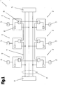
- Fig.1 is a conventional structure of an inverter system 1 with several - here six - parallel connected at the output inverter 2 shown. Since the individual components or assemblies and functions of inverters 2 are already known from the prior art, they will not be discussed in detail below.
- the inverters 2 include, for example, a DC-DC converter, a DC link, and a DC-AC converter (not shown).
- a power source 3 or a power generator is connected, which can be formed, for example, of one or more parallel and / or series-connected solar modules or a battery.
- the output of each inverter 2 is over AC power network or a multi-phase network 4, for example a 3-phase network, connected to one or more electrical loads 5.
- the load 5 is constituted by an engine, a refrigerator, a radio, and so on.
- the inverter system 1 is used as an island inverter system for supplying decoupled from the public power grid consumers 5.
- the failure probability of the inverter system 1 can be reduced due to the redundant design, as a result of which critical loads 5 can be supplied with energy fail-safe.
- an inverter 2 Des.Werneren, an inverter 2, a control device 6, which may be formed for example by a microprocessor, a microcontroller or a computer, via which a corresponding control of the individual modules, in particular the switching elements arranged therein, can be made.
- the individual control or control processes are stored by appropriate software programs and / or data or characteristics.
- the in Fig. 1 The construction shown with the inverters 2 connected in parallel preferably serves to ensure a defined distribution of the power required by the consumer (s) 5 to the individual inverters 2.
- the inverters 2 are of identical construction, so that a symmetrical or even load distribution between the inverters 2 can take place.
- inverters 2 of different types for example different power classes or rated power, in parallel operation, in which case a corresponding proportionate load distribution, which depends in particular on the rated power, on the inverters 2.
- the inverter system 1 is controlled such that the second Inverter 2 also twice the power to the consumer or 5 delivers.
- the inverters 2 are connected to one another via at least one data line 7, for example an optical waveguide, for signal or data exchange.
- the inverters 2 have communication devices 8, which accordingly Fig. 2 a transmitting device 9 and a receiving device 10, which are connected via a transmission line 11 and a receiving line 12 to the control device 6.
- the inverters 2 are synchronized via this data line 7 during operation in such a way that the sinusoidal alternating voltages at the outputs of the inverters 2 are in common phase, that is, have the same zero crossings. Accordingly, a correspondingly fast communication via the data line 7 is required for this purpose.
- the data lines 7 are also used for safely starting up the inverter system 1, for which purpose completely contradictory requirements are required for the type of data transmission as for synchronization. Accordingly, a high transmission reliability for detecting all inverters 2 in the inverter system 1 must be ensured.
- a switching device 13 is integrated in the communication device 8 of the inverter 2.
- This switching device 13 and the corresponding method for switching between a ring system and a bus system will be subsequently in synopsis of Fig. 1 .
- Fig. 2 and Fig. 3 described in more detail.
- the switching device 13 is thus integrated into the communication device 8 such that the transmission line 11 and the receiving line 12 can be interrupted or switched correspondingly to the control device 6.
- the switching device 13 is preferably formed by a CMOS logic device, a relay, an Erasable Programmable Logic Device (EPLD), simple analog switches, or the like.
- EPLD Erasable Programmable Logic Device
- the data line 7 between the inverters 2 is physically realized as a ring system or a ring topology. That is, each inverter 2 is connected to two adjacent inverters 2. In this case, the data or the data packets are transferred stepwise from one inverter 2 to the next, wherein each inverter 2 has to evaluate the data before it can forward it.
- the switching device 13 is connected such that the transmission line 11 of the transmitting device 9 is connected to a transmission line 14 of the control device 6, and the receiving line 12 of the receiving device 10 is connected to the receiving line 15 of the control device 6.
- a switch 17 which is actuated by the control device 6 via a control line 16 and which connects the transmission line 11 to the transmission line 14 is closed.
- a further switch 18, which connects the receiving line 12 to the transmission line 11, driven, which acts inversely to the switch 17, that is opened in this case.
- the inverter 2 uses the ring system for communication.
- the switch 17 and the switch 18 is formed only by a switch, for example, the switch 17.
- the switch 17 serves as a switch, which simply connects the transmission line 11 with either the transmission line 14 or the receiving line 12. Since the ring system ensures a high transmission reliability of the data, it is thus ensured that all inverters 2 are detected when the inverter system 1 is started up.
- an inverter 2 defined as the master for example, during the first startup of the inverter system 1, is the first to send a reset data packet.
- This causes all inverters 2 to be switched to the ring topology required for booting if they are not already in the ring topology.
- the master in the inverter system 1 can also be determined automatically. For example, that inverter 2 can be designated as master, which first sends a data packet.
- the master After sending the reset data packet, the master sends another data packet, for example a so-called bus init packet.
- the bus-init packet is routed via the receiving device 10, receiving line 12, switching device 13 and the receiving line 15 to the control device 6 of the inverter 2 and evaluated.
- the control device 6 Before the bus init packet is now sent via the transmission line 14, the switching device 13, the transmission line 11 and the transmitting device 9 via the data line 7 to the next inverter 2, the control device 6 is a so-called.
- Inverter ID or a Initialization package attached to the bus init packet of the master.
- the next inverter 2 receives the Bus Init packet supplemented with an inverter ID and also supplements it with its inverter ID.
- the master receives the bus init packet it has sent out, corresponding to the attached inverter IDs. Due to the number of inverter IDs attached, the master knows how many inverters 2 are in the inverter system 1. Likewise, with the receipt of the bus init packet, it is ensured that all inverters 2 are also ready for operation and the master is informed about the configuration of the individual inverters 2. Such information is preferably included in the inverter ID, which is formed for example by the serial number, the serial number in combination with the software number, etc. of the inverter 2. The inverter ID also ensures that each inverter 2 in the inverter system 1 is clearly addressable, and this can be done without predefined addressing. For example, an inverter 2 can also be clearly addressed via the physical position in the inverter system 1.
- the communication takes place during operation of the inverter system 1 via the bus topology, whereby a much faster transmission speed, in particular for the synchronization is given.
- the data transmission in the bus topology preferably takes place serially and asynchronously. This means that the bits that make up a data packet are transmitted one after the other, with a start bit before the eight data bits, for example, and a stop bit after the data bits. Since the data transmission in the control device 6 is usually parallel, a serial-to-parallel conversion is required. This takes place, for example, via a UART (Universal Asynchronous Receiver Transmitter), to which the transmission line 14 and the reception line 15 are therefore connected.
- UART Universal Asynchronous Receiver Transmitter
- each inverter 2 is assigned a time window in which it is allowed to send data packets to the data line 7 or to the bus. Between the time windows there is preferably a period of time in which no inverter 2 transmits.
- only one inverter 2 in the inverter system 1 always transmits, with its transmitted data being received substantially immediately by the remaining inverters 2, before it is even allowed to the next inverter 2 in its time window to send its data onto the bus. This prevents data collisions and guarantees secure and fast communication.
- the inverter system 1 Due to the switching process, the inverter system 1 is now located in the bus topology, which is logically based on the ring system. Therefore, even in the bus system, the data transmission is unidirectional and not bidirectional, as is common in bus systems of the prior art.
- the combination of the transmission reliability for detecting the inverter 2 in the system with the high data transmission speed during operation has a much greater importance.
- the delay times for the data transmission from one inverter 2 to the adjacent inverter 2, the data being transmitted via all further inverters 2, are negligible. Thus, it can be readily spoken of a data transmission without time delay.
- all inverters 2 in the system 1 automatically receive the data packet, since the data packet is received by the receiving device 10, is transmitted via the receiving line 12, the switch 18 and the transmission line 11 to the transmitting device 9 and is forwarded accordingly to the next inverter 2. That is, there is no evaluation of the data by the control device 6 before a forwarding of the data is performed. According to the structure of the switching device 13, however, the received data packet is also routed via the receiving line 15 to the control device 6. As a result, they can evaluate the data packet, so to speak without time pressure, and process it if necessary, if it is intended for this inverter 2.
- an inverter 2 or its control device 6 In order for an inverter 2 or its control device 6 to be able to respond to a data packet intended for it, the latter must wait for the time slot assigned to it. For transmission in the time window, it is now necessary to separate the receiving line 12 by opening the switch 18 from the transmission line 11. At the same time, the switch 17 is closed with this process via the control line 16, and thus the transmission line 14 is connected to the transmission line 11. Thus, the controller 6 can send its response to the bus. Immediately after the transmission, the switches 17, 18 are switched over the control line 16 again and the receiving line 12 is again connected to the transmission line 11.
- the control device 6 sends a reset data packet to the bus. As a result, all the inverters 2 in the system 1 switch to the ring system, so that the system 1 can be restarted.
- an automatic closing mechanism with an independent power supply is integrated in the inverter 2. This means that, for example, in the event of a power failure at an inverter 2, the communication in the system 1 is not interrupted. As a result, the switching device 13 is permanently switched to the bus system, so that the data line 7 remains.
- the automatic locking mechanism can be triggered by a retriggerable Monoflop be realized.
- inverter 2 is connected to which phase in a multi-phase network, for example the 3-phase network 4.
- this is done such that an inverter 2 applies a voltage to the phase.
- This is carried out correspondingly for each phase, whereby preferably that inverter 2 is allowed to apply the voltage to the phase which carries this out first. Accordingly, the information between the inverters 2 can then be exchanged, which inverter 2 is connected to which phase of the 3-phase network 4.
- the inverters 2 know how many more inverters 2 are also connected to the same phase, which is important for a defined division of the load or the consumer 5 and for the synchronization of the inverter 2.
- a completely automatic configuration of the inverter system 1 enables a completely automatic configuration of the inverter system 1.
Landscapes
- Engineering & Computer Science (AREA)
- Power Engineering (AREA)
- Small-Scale Networks (AREA)
Claims (13)
- Système d'onduleurs (1) comprenant plusieurs onduleurs (2), qui comprennent chacun au moins un dispositif de commande (6), au moins une ligne (7) étant agencée à chaque fois entre les onduleurs (2) pour l'échange de données, caractérisé en ce que les lignes de données (7) entre les onduleurs (2) sont réalisées par des conducteurs de lumière, en ce que chaque onduleur (2) comprend un dispositif de communication (8) raccordé avec le dispositif de commande (6) de l'onduleur (2) et les lignes de données (7) de deux onduleurs voisins (2), comprenant un dispositif de commutation (13), un dispositif d'envoi (9) et un dispositif de réception (10), le dispositif d'envoi (9) étant raccordé par une ligne d'envoi (11) et le dispositif de réception (10) par une ligne de réception (12) avec le dispositif de commutation (13), et le dispositif d'envoi (9) d'un onduleur (2) étant raccordé avec le dispositif de réception (10) de l'onduleur (2) suivant et le dispositif de réception (10) de l'onduleur (2) avec le dispositif d'envoi (9) de l'onduleur (2) précédent, le dispositif de commutation (13) de chaque onduleur (2) étant configuré pour la commutation des lignes de données (7) par un paquet de données de commutation provenant d'un onduleur (2) défini comme maître, transférable graduellement et unidirectionnellement d'un onduleur (2) vers l'onduleur (2) suivant, entre un système de circuit utilisé pendant le processus de démarrage du système d'onduleurs (1), selon lequel tous les onduleurs (2) sont raccordés ensemble par les lignes de données (7) en un circuit et les données sont évaluées par le dispositif de commande (6) de chaque onduleur (2) avant le transfert vers l'onduleur (2) suivant, et un système de bus fondé de manière logique sur le système de circuit après la fin du processus de démarrage pendant une exploitation en cours du système d'onduleurs (1), selon lequel tous les onduleurs (2) sont reliés par un bus commun formé par les lignes de données (7) et les données sont envoyées essentiellement simultanément et directement à tous les onduleurs (2), puis les données sont évaluées par les dispositifs de commande (6) de tous les onduleurs (2), une fenêtre de temps pour l'envoi de données dans la ligne de données (7) pouvant être attribuée au paquet de données de commutation de chaque onduleur, et la ligne de réception (12) étant séparée de la ligne d'envoi (11) pour l'envoi dans la fenêtre de temps.
- Système d'onduleurs (1) selon la revendication 1, caractérisé en ce que le dispositif de commutation (13) de chaque onduleur (2) est raccordé avec ledit au moins un dispositif de commande (6) par au moins une ligne d'envoi (14) et une ligne de réception (15).
- Système d'onduleurs (1) selon la revendication 2, caractérisé en ce que la ligne de réception (15) du dispositif de commande (6) est raccordée en permanence par le biais du dispositif de commutation (13) avec la ligne de réception (12) du dispositif de réception (10), et la ligne d'envoi (11) peut être raccordée par le biais du dispositif de commutation (13) au choix avec la ligne d'envoi (14) du dispositif de commande (6) ou la ligne de réception (12) du dispositif de réception (10).
- Système d'onduleurs (1) selon l'une quelconque des revendications 1 à 3, caractérisé en ce que le dispositif de commutation (13) de chaque onduleur (2) contient au moins un commutateur (17) qui est raccordé par une ligne de commande (16) avec le dispositif de commande (6) de l'onduleur (2).
- Onduleur (2) pour un système d'onduleurs (1) selon l'une quelconque des revendications 1 à 4, qui comprend au moins un dispositif de commande (6) et des raccords pour des lignes (7) pour le raccordement avec d'autres onduleurs (2) pour l'échange de données, caractérisé en ce qu'un dispositif de communication (8) raccordé avec le dispositif de commande (6) et les raccords pour les lignes de données (7) réalisées par des conducteurs de lumière est muni d'un dispositif de commutation (13), d'un dispositif d'envoi (9) et d'un dispositif de réception (10), le dispositif d'envoi (9) étant raccordé par une ligne d'envoi (11) et le dispositif de réception (10) par une ligne de réception (12) avec le dispositif de commutation (13), et le dispositif d'envoi (9) pouvant être raccordé avec le dispositif de réception (10) d'un onduleur suivant (2) et le dispositif de réception (10) avec le dispositif d'envoi (9) d'un onduleur précédent (2), le dispositif de commutation (13) étant configuré pour la commutation des lignes de données (7) par un paquet de données de commutation provenant d'un onduleur (2) défini comme maître, transférable graduellement et unidirectionnellement vers l'onduleur (2) suivant, entre un système de circuit utilisé pendant le processus de démarrage du système d'onduleurs (1), selon lequel tous les onduleurs (2) sont raccordés ensemble par les lignes de données (7) en un circuit et les données sont évaluées par le dispositif de commande (6) de chaque onduleur (2) avant le transfert vers l'onduleur (2) suivant, et un système de bus fondé de manière logique sur le système de circuit après la fin du processus de démarrage pendant une exploitation en cours du système d'onduleurs (1), selon lequel tous les onduleurs (2) sont reliés par un bus commun formé par les lignes de données (7) et les données sont envoyées essentiellement simultanément et directement à tous les onduleurs (2), puis les données sont évaluées par les dispositifs de commande (6) de tous les onduleurs (2), une fenêtre de temps pour l'envoi de données dans la ligne de données (7) pouvant être attribuée au paquet de données de commutation de l'onduleur (2) , et la ligne de réception (12) étant séparée de la ligne d'envoi (11) pour l'envoi dans la fenêtre de temps.
- Onduleur (2) selon la revendication 5, caractérisé en ce que le dispositif de commutation (13) est raccordé avec ledit au moins un dispositif de commande (6) par au moins une ligne d'envoi (14) et une ligne de réception (15).
- Onduleur (2) selon la revendication 6, caractérisé en ce que la ligne de réception (15) du dispositif de commande (6) est raccordée en permanence par le biais du dispositif de commutation (13) avec la ligne de réception (12) du dispositif de réception (10), et la ligne d'envoi (11) peut être raccordée par le biais du dispositif de commutation (13) au choix avec la ligne d'envoi (14) du dispositif de commande (6) ou la ligne de réception (12) du dispositif de réception (10).
- Onduleur (2) selon l'une quelconque des revendications 5 à 7, caractérisé en ce que le dispositif de commutation (13) contient au moins un commutateur (17) qui est raccordé par une ligne de commande (16) avec le dispositif de commande (6).
- Procédé d'exploitation de plusieurs onduleurs (2) comprenant à chaque fois un dispositif de commande (6) d'un système d'onduleurs (1), des données étant échangées entre les onduleurs (2) par au moins une ligne (7), caractérisé en ce que les lignes de données (7) réalisées par des conducteurs de lumière sont raccordées avec à chaque fois un dispositif d'envoi (9) et à chaque fois un dispositif de réception (10) d'un dispositif de communication (8) de chaque onduleur (2), en ce que le dispositif d'envoi (9) d'un onduleur (2) est raccordé avec le dispositif de réception (10) de l'onduleur suivant (2) et le dispositif de réception (10) de l'onduleur (2) avec le dispositif d'envoi (9) de l'onduleur précédent (2), en ce que le dispositif d'envoi (9) de chaque onduleur (2) est raccordé par une ligne d'envoi (11) et le dispositif de réception (10) de chaque onduleur (2) par une ligne de réception (12) avec un dispositif de commutation (13), pendant un processus de démarrage du système d'onduleurs (1), les onduleurs (2) sont reliés par le dispositif de commutation (13) en un système de circuit physique et logique, selon lequel tous les onduleurs (2) sont raccordés ensemble par les lignes de données (7) en un circuit et les données sont évaluées par le dispositif de commande (6) de chaque onduleur (2) avant le transfert vers l'onduleur (2) suivant, et en ce qu'après le processus de démarrage, pendant une exploitation en cours, le raccordement des onduleurs (2) est commuté par un paquet de données de commutation provenant d'un onduleur (2) défini comme maître, transférable graduellement et unidirectionnellement d'un onduleur (2) vers l'onduleur (2) suivant par un système de bus fondé de manière logique sur le système de circuit, selon lequel tous les onduleurs (2) sont reliés par un bus commun formé par les lignes de données (7) et les données sont envoyées essentiellement simultanément et directement à tous les onduleurs (2), puis les données sont évaluées par les dispositifs de commande (6) de tous les onduleurs (2), une fenêtre de temps pour l'envoi de données dans la ligne de données (7) pouvant être attribuée au paquet de données de commutation de chaque onduleur, et la ligne de réception (12) étant séparée de la ligne d'envoi (11) pour l'envoi dans la fenêtre de temps.
- Procédé selon la revendication 9, caractérisé en ce que, pendant le processus de démarrage, un onduleur (2) est défini comme maître, et une initialisation de l'onduleur (2) le système d'onduleurs (1) est réalisée à partir de l'onduleur (2) défini comme maître.
- Procédé selon la revendication 10, caractérisé en ce qu'un paquet de données est envoyé à partir de l'onduleur (2) défini comme maître vers l'onduleur (2) raccordé à celui-ci, et le paquet de données est complété par un paquet d'initialisation avant d'être transféré vers l'onduleur (2) suivant.
- Procédé selon la revendication 10 ou 11, caractérisé en ce que le paquet de données est transféré d'un onduleur (2) vers l'onduleur (2) suivant dans le système de circuit jusqu'à ce que le paquet de données soit de nouveau reçu par l'onduleur (2) défini comme maître.
- Procédé selon l'une quelconque des revendications 10 à 12, caractérisé en ce que, pendant le processus de démarrage, on vérifie quel onduleur (2) est raccordé à quelle phase d'un réseau polyphasé (4), et en ce que les onduleurs (2) sont synchronisés selon cette vérification.
Applications Claiming Priority (2)
| Application Number | Priority Date | Filing Date | Title |
|---|---|---|---|
| AT0161606A AT504120B1 (de) | 2006-09-28 | 2006-09-28 | Wechselrichtersystem, wechselrichter und verfahren zum betreiben von wechselrichtern eines wechselrichtersystems |
| PCT/AT2007/000441 WO2008036990A1 (fr) | 2006-09-28 | 2007-09-17 | Échange de données entre onduleurs dans un système d'onduleurs |
Publications (2)
| Publication Number | Publication Date |
|---|---|
| EP2067247A1 EP2067247A1 (fr) | 2009-06-10 |
| EP2067247B1 true EP2067247B1 (fr) | 2016-04-13 |
Family
ID=38896944
Family Applications (1)
| Application Number | Title | Priority Date | Filing Date |
|---|---|---|---|
| EP07800185.6A Not-in-force EP2067247B1 (fr) | 2006-09-28 | 2007-09-17 | Échange de données entre onduleurs dans un système d'onduleurs |
Country Status (6)
| Country | Link |
|---|---|
| US (1) | US8456877B2 (fr) |
| EP (1) | EP2067247B1 (fr) |
| CN (1) | CN101523714B (fr) |
| AT (1) | AT504120B1 (fr) |
| AU (1) | AU2007302609B2 (fr) |
| WO (1) | WO2008036990A1 (fr) |
Cited By (1)
| Publication number | Priority date | Publication date | Assignee | Title |
|---|---|---|---|---|
| DE102021203615A1 (de) | 2021-04-13 | 2022-10-13 | Fronius International Gmbh | Bidirektionaler Wechselrichter |
Families Citing this family (15)
| Publication number | Priority date | Publication date | Assignee | Title |
|---|---|---|---|---|
| TW201010239A (en) * | 2008-04-22 | 2010-03-01 | Array Converter Inc | High voltage array converter |
| JP5160371B2 (ja) | 2008-10-17 | 2013-03-13 | 本田技研工業株式会社 | 交流電力供給装置及びその制御方法 |
| AT508104B1 (de) * | 2009-02-12 | 2015-05-15 | Fronius Int Gmbh | Photovoltaikanlage mit mehreren wechselrichtern, wechselrichter, usb-massenspeichergerät und verfahren zum durchführen von software-updates an wechselrichtern |
| US8482156B2 (en) * | 2009-09-09 | 2013-07-09 | Array Power, Inc. | Three phase power generation from a plurality of direct current sources |
| US20110138377A1 (en) * | 2010-05-04 | 2011-06-09 | Phat Energy Corporation | Renewable Energy Monitoring System & Method |
| US9160408B2 (en) | 2010-10-11 | 2015-10-13 | Sunpower Corporation | System and method for establishing communication with an array of inverters |
| KR101779614B1 (ko) * | 2011-06-08 | 2017-09-18 | 엘에스산전 주식회사 | 인버터 통신 시스템 |
| WO2013067429A1 (fr) | 2011-11-03 | 2013-05-10 | Arraypower, Inc. | Conversion de courant continu en courant alternatif utilisant une modulation de phase intermédiaire |
| DE102012211605A1 (de) * | 2012-07-04 | 2014-01-09 | Siemens Aktiengesellschaft | Photovoltaikanlage |
| WO2016165718A1 (fr) * | 2015-04-16 | 2016-10-20 | Vestas Wind Systems A/S | Contrôle d'un système de convertisseur d'une éolienne sur un bus de communication |
| DE102015210918A1 (de) * | 2015-06-15 | 2016-12-15 | TRUMPF Hüttinger GmbH + Co. KG | Inverter zum Laden und/oder Entladen von Batterien |
| CN108476153B (zh) * | 2016-01-15 | 2021-02-19 | 东芝三菱电机产业系统株式会社 | 控制系统 |
| US11108243B1 (en) * | 2020-05-06 | 2021-08-31 | Hong Liu Co., Ltd. | Switching AC/DC power supply system with 10MHz time base |
| US12194858B2 (en) | 2021-10-20 | 2025-01-14 | Toyota Motor Engineering & Manufacturing North America, Inc. | Systems and methods for providing power to an electric motor from an inverter |
| US12081140B2 (en) * | 2022-04-06 | 2024-09-03 | Ge Energy Power Conversion Technology Limited | Switching synchronization for modular multilevel converters |
Family Cites Families (16)
| Publication number | Priority date | Publication date | Assignee | Title |
|---|---|---|---|---|
| DE2904786C2 (de) * | 1979-02-08 | 1981-02-19 | Siemens Ag, 1000 Berlin Und 8000 Muenchen | Verfahren zur Regelung von Wechselrichtern im Parallelbetrieb und Schaltungsanordnungen zur Durchführung des Verfahrens |
| US5191520A (en) * | 1989-02-06 | 1993-03-02 | Boral Johns Perry Industries Pty. Ltd. | Power supply system |
| JP2679411B2 (ja) * | 1990-12-19 | 1997-11-19 | 三菱電機株式会社 | 交流出力変換器の並列運転制御装置 |
| TW245848B (fr) * | 1991-09-18 | 1995-04-21 | Toshiba Kk | |
| DE10153846B4 (de) * | 2001-11-02 | 2004-11-25 | Daimlerchrysler Ag | Zünd- oder Einspritzmodul und zugehörendes Initialisierungsverfahren |
| BR0300173A (pt) * | 2003-01-31 | 2004-10-26 | Engetron Engenharia Eletronica | Sistema de suprimento de energia com operação em paralelo de inversores monofásicos ou polifásicos |
| DE10336301A1 (de) * | 2003-07-31 | 2005-03-10 | Ego Elektro Geraetebau Gmbh | Verfahren zur dynamischen Vergabe von Adressen sowie zugehörige Verwendung für Heizeinrichtungen |
| US20050073783A1 (en) * | 2003-10-02 | 2005-04-07 | Phoenixtec Power Co., Ltd. | Parallel redundant power system and the control method for the same |
| DE102004015227A1 (de) * | 2004-03-24 | 2005-10-27 | Siemens Ag | Elektrisches Feldgerät |
| DE102004025923A1 (de) * | 2004-05-27 | 2005-12-22 | Siemens Ag | Photovoltaikanlage zur Einspeisung in ein elektrisches Netz sowie zentrales Steuer- und Überwachungsgerät für eine Photovoltaikanlage |
| DE102004030228B4 (de) * | 2004-06-23 | 2008-06-19 | Siemens Ag | Schaltung von Pulswechselrichtern bei Bahnfahrzeugen |
| US7502240B2 (en) * | 2004-07-27 | 2009-03-10 | Silicon Laboratories Inc. | Distributed power supply system with separate SYNC control for controlling remote digital DC/DC converters |
| AT501542B1 (de) * | 2004-12-16 | 2009-03-15 | Fronius Int Gmbh | Verfahren zur erkennung der last eines inselwechselrichters und inselwechselrichter |
| AT501422B1 (de) | 2005-02-10 | 2009-05-15 | Fronius Int Gmbh | Wechselrichtersystem zum einspeisen in ein 3-phasennetz sowie wechselrichteranlage für ein 3-phasennetz |
| US7593243B2 (en) * | 2006-10-09 | 2009-09-22 | Honeywell International Inc. | Intelligent method for DC bus voltage ripple compensation for power conversion units |
| AT508104B1 (de) * | 2009-02-12 | 2015-05-15 | Fronius Int Gmbh | Photovoltaikanlage mit mehreren wechselrichtern, wechselrichter, usb-massenspeichergerät und verfahren zum durchführen von software-updates an wechselrichtern |
-
2006
- 2006-09-28 AT AT0161606A patent/AT504120B1/de not_active IP Right Cessation
-
2007
- 2007-09-17 AU AU2007302609A patent/AU2007302609B2/en not_active Ceased
- 2007-09-17 WO PCT/AT2007/000441 patent/WO2008036990A1/fr not_active Ceased
- 2007-09-17 US US12/311,370 patent/US8456877B2/en not_active Expired - Fee Related
- 2007-09-17 EP EP07800185.6A patent/EP2067247B1/fr not_active Not-in-force
- 2007-09-17 CN CN2007800363145A patent/CN101523714B/zh not_active Expired - Fee Related
Cited By (1)
| Publication number | Priority date | Publication date | Assignee | Title |
|---|---|---|---|---|
| DE102021203615A1 (de) | 2021-04-13 | 2022-10-13 | Fronius International Gmbh | Bidirektionaler Wechselrichter |
Also Published As
| Publication number | Publication date |
|---|---|
| CN101523714B (zh) | 2012-12-05 |
| US8456877B2 (en) | 2013-06-04 |
| US20090290393A1 (en) | 2009-11-26 |
| AT504120A4 (de) | 2008-03-15 |
| AU2007302609A1 (en) | 2008-04-03 |
| CN101523714A (zh) | 2009-09-02 |
| WO2008036990A1 (fr) | 2008-04-03 |
| AU2007302609B2 (en) | 2011-11-03 |
| AT504120B1 (de) | 2008-03-15 |
| EP2067247A1 (fr) | 2009-06-10 |
Similar Documents
| Publication | Publication Date | Title |
|---|---|---|
| WO2008036990A1 (fr) | Échange de données entre onduleurs dans un système d'onduleurs | |
| EP2720098B1 (fr) | Système de sécurité pour une installation comprenant un chemin de signal de test avec un chemin de retour | |
| EP1064759B1 (fr) | Procede de mise en service d'un systeme bus et systeme bus en question | |
| DE19718284C2 (de) | Verfahren und Vorrichtung zum Überwachen einer Anlage mit mehreren Funktionseinheiten | |
| DE2626838C3 (de) | Prüf-Schaltungsanordnung für eine duplizierte Fernmeldeinstallation | |
| DE102020129135B3 (de) | Verfahren und System zum Verwenden eines Hochgeschwindigkeitsbusses in einer Wechselstrombatterie | |
| DE2362344B2 (de) | Datenuebertragungsanlage | |
| DE3236812A1 (de) | Fernwirksystem | |
| EP0092719B1 (fr) | Disposition pour le couplage d'unités de traitement numérique | |
| DE102016000126B4 (de) | Serielles Bussystem mit Koppelmodulen | |
| EP2557657A2 (fr) | Système d'éclairage d'urgence et procédé pour son alimentation | |
| EP0192120B1 (fr) | Système et dispositif de transmission de données pour commande à distance | |
| DE102008017533C5 (de) | Sicherheitsbeleuchtungsanlage mit einem Splitter | |
| EP2704332B1 (fr) | Installation d'éclairage de secours/de sécurité et son procédé de commande | |
| WO2009156122A1 (fr) | Système de surveillance | |
| DE19916894A1 (de) | Bussystem | |
| DE102013109090B9 (de) | Energieverteilungseinheit, Computeranordnung und Verfahren zum Erfassen von Anschlussinformationen | |
| DE102008037610A1 (de) | Vorrichtung und Verfahren zur wahlweisen Umschaltung zweier Master für zugeordnete Slaves | |
| EP2255498B1 (fr) | Autorisation de fonctionnement d'unités d'automatisation reliées à une installation et installation correspondante | |
| EP0680232A2 (fr) | Procédé pour la configuration d'un réseau informatique | |
| DE3211020C1 (de) | Übertragungs-Einrichtung zur Datenübermittlung zwischen einer Steuerzentrale und mehreren Regel- oder Steuergeräten eines Gebäudes | |
| EP1734455B1 (fr) | Adressage d'une unité esclave dans un système maître-esclave | |
| EP1196829B1 (fr) | Module de commande d'un mecanisme d'entrainement | |
| EP3861636A1 (fr) | Procédé de commande de semi-conducteurs | |
| DE102011083473A1 (de) | Kommunikationsschnittstelle zur Systemüberwachung der Energieversorgung in Elektro- und Hybridfahrzeugen |
Legal Events
| Date | Code | Title | Description |
|---|---|---|---|
| PUAI | Public reference made under article 153(3) epc to a published international application that has entered the european phase |
Free format text: ORIGINAL CODE: 0009012 |
|
| 17P | Request for examination filed |
Effective date: 20090415 |
|
| AK | Designated contracting states |
Kind code of ref document: A1 Designated state(s): AT BE BG CH CY CZ DE DK EE ES FI FR GB GR HU IE IS IT LI LT LU LV MC MT NL PL PT RO SE SI SK TR |
|
| RIN1 | Information on inventor provided before grant (corrected) |
Inventor name: ANGERER, CHRISTIAN Inventor name: HEIGL, HANNES Inventor name: KREUZER, HARALD |
|
| 17Q | First examination report despatched |
Effective date: 20091221 |
|
| DAX | Request for extension of the european patent (deleted) | ||
| GRAP | Despatch of communication of intention to grant a patent |
Free format text: ORIGINAL CODE: EPIDOSNIGR1 |
|
| INTG | Intention to grant announced |
Effective date: 20151112 |
|
| GRAS | Grant fee paid |
Free format text: ORIGINAL CODE: EPIDOSNIGR3 |
|
| GRAA | (expected) grant |
Free format text: ORIGINAL CODE: 0009210 |
|
| RAP1 | Party data changed (applicant data changed or rights of an application transferred) |
Owner name: FRONIUS INTERNATIONAL GMBH |
|
| AK | Designated contracting states |
Kind code of ref document: B1 Designated state(s): AT BE BG CH CY CZ DE DK EE ES FI FR GB GR HU IE IS IT LI LT LU LV MC MT NL PL PT RO SE SI SK TR |
|
| REG | Reference to a national code |
Ref country code: GB Ref legal event code: FG4D Free format text: NOT ENGLISH |
|
| REG | Reference to a national code |
Ref country code: AT Ref legal event code: REF Ref document number: 791069 Country of ref document: AT Kind code of ref document: T Effective date: 20160415 Ref country code: CH Ref legal event code: EP |
|
| REG | Reference to a national code |
Ref country code: IE Ref legal event code: FG4D Free format text: LANGUAGE OF EP DOCUMENT: GERMAN |
|
| REG | Reference to a national code |
Ref country code: DE Ref legal event code: R096 Ref document number: 502007014717 Country of ref document: DE |
|
| REG | Reference to a national code |
Ref country code: LT Ref legal event code: MG4D |
|
| REG | Reference to a national code |
Ref country code: NL Ref legal event code: MP Effective date: 20160413 |
|
| REG | Reference to a national code |
Ref country code: FR Ref legal event code: PLFP Year of fee payment: 10 |
|
| PG25 | Lapsed in a contracting state [announced via postgrant information from national office to epo] |
Ref country code: NL Free format text: LAPSE BECAUSE OF FAILURE TO SUBMIT A TRANSLATION OF THE DESCRIPTION OR TO PAY THE FEE WITHIN THE PRESCRIBED TIME-LIMIT Effective date: 20160413 Ref country code: FI Free format text: LAPSE BECAUSE OF FAILURE TO SUBMIT A TRANSLATION OF THE DESCRIPTION OR TO PAY THE FEE WITHIN THE PRESCRIBED TIME-LIMIT Effective date: 20160413 Ref country code: PL Free format text: LAPSE BECAUSE OF FAILURE TO SUBMIT A TRANSLATION OF THE DESCRIPTION OR TO PAY THE FEE WITHIN THE PRESCRIBED TIME-LIMIT Effective date: 20160413 Ref country code: LT Free format text: LAPSE BECAUSE OF FAILURE TO SUBMIT A TRANSLATION OF THE DESCRIPTION OR TO PAY THE FEE WITHIN THE PRESCRIBED TIME-LIMIT Effective date: 20160413 |
|
| PG25 | Lapsed in a contracting state [announced via postgrant information from national office to epo] |
Ref country code: ES Free format text: LAPSE BECAUSE OF FAILURE TO SUBMIT A TRANSLATION OF THE DESCRIPTION OR TO PAY THE FEE WITHIN THE PRESCRIBED TIME-LIMIT Effective date: 20160413 Ref country code: LV Free format text: LAPSE BECAUSE OF FAILURE TO SUBMIT A TRANSLATION OF THE DESCRIPTION OR TO PAY THE FEE WITHIN THE PRESCRIBED TIME-LIMIT Effective date: 20160413 Ref country code: GR Free format text: LAPSE BECAUSE OF FAILURE TO SUBMIT A TRANSLATION OF THE DESCRIPTION OR TO PAY THE FEE WITHIN THE PRESCRIBED TIME-LIMIT Effective date: 20160714 Ref country code: PT Free format text: LAPSE BECAUSE OF FAILURE TO SUBMIT A TRANSLATION OF THE DESCRIPTION OR TO PAY THE FEE WITHIN THE PRESCRIBED TIME-LIMIT Effective date: 20160816 Ref country code: SE Free format text: LAPSE BECAUSE OF FAILURE TO SUBMIT A TRANSLATION OF THE DESCRIPTION OR TO PAY THE FEE WITHIN THE PRESCRIBED TIME-LIMIT Effective date: 20160413 |
|
| REG | Reference to a national code |
Ref country code: DE Ref legal event code: R097 Ref document number: 502007014717 Country of ref document: DE |
|
| PG25 | Lapsed in a contracting state [announced via postgrant information from national office to epo] |
Ref country code: DK Free format text: LAPSE BECAUSE OF FAILURE TO SUBMIT A TRANSLATION OF THE DESCRIPTION OR TO PAY THE FEE WITHIN THE PRESCRIBED TIME-LIMIT Effective date: 20160413 Ref country code: RO Free format text: LAPSE BECAUSE OF FAILURE TO SUBMIT A TRANSLATION OF THE DESCRIPTION OR TO PAY THE FEE WITHIN THE PRESCRIBED TIME-LIMIT Effective date: 20160413 Ref country code: EE Free format text: LAPSE BECAUSE OF FAILURE TO SUBMIT A TRANSLATION OF THE DESCRIPTION OR TO PAY THE FEE WITHIN THE PRESCRIBED TIME-LIMIT Effective date: 20160413 Ref country code: SK Free format text: LAPSE BECAUSE OF FAILURE TO SUBMIT A TRANSLATION OF THE DESCRIPTION OR TO PAY THE FEE WITHIN THE PRESCRIBED TIME-LIMIT Effective date: 20160413 Ref country code: CZ Free format text: LAPSE BECAUSE OF FAILURE TO SUBMIT A TRANSLATION OF THE DESCRIPTION OR TO PAY THE FEE WITHIN THE PRESCRIBED TIME-LIMIT Effective date: 20160413 |
|
| PLBE | No opposition filed within time limit |
Free format text: ORIGINAL CODE: 0009261 |
|
| STAA | Information on the status of an ep patent application or granted ep patent |
Free format text: STATUS: NO OPPOSITION FILED WITHIN TIME LIMIT |
|
| PG25 | Lapsed in a contracting state [announced via postgrant information from national office to epo] |
Ref country code: BE Free format text: LAPSE BECAUSE OF NON-PAYMENT OF DUE FEES Effective date: 20160930 |
|
| 26N | No opposition filed |
Effective date: 20170116 |
|
| PG25 | Lapsed in a contracting state [announced via postgrant information from national office to epo] |
Ref country code: MC Free format text: LAPSE BECAUSE OF FAILURE TO SUBMIT A TRANSLATION OF THE DESCRIPTION OR TO PAY THE FEE WITHIN THE PRESCRIBED TIME-LIMIT Effective date: 20160413 |
|
| REG | Reference to a national code |
Ref country code: CH Ref legal event code: PL |
|
| PG25 | Lapsed in a contracting state [announced via postgrant information from national office to epo] |
Ref country code: SI Free format text: LAPSE BECAUSE OF FAILURE TO SUBMIT A TRANSLATION OF THE DESCRIPTION OR TO PAY THE FEE WITHIN THE PRESCRIBED TIME-LIMIT Effective date: 20160413 |
|
| REG | Reference to a national code |
Ref country code: IE Ref legal event code: MM4A |
|
| PG25 | Lapsed in a contracting state [announced via postgrant information from national office to epo] |
Ref country code: IE Free format text: LAPSE BECAUSE OF NON-PAYMENT OF DUE FEES Effective date: 20160917 Ref country code: CH Free format text: LAPSE BECAUSE OF NON-PAYMENT OF DUE FEES Effective date: 20160930 Ref country code: LI Free format text: LAPSE BECAUSE OF NON-PAYMENT OF DUE FEES Effective date: 20160930 |
|
| PG25 | Lapsed in a contracting state [announced via postgrant information from national office to epo] |
Ref country code: LU Free format text: LAPSE BECAUSE OF NON-PAYMENT OF DUE FEES Effective date: 20160917 |
|
| REG | Reference to a national code |
Ref country code: FR Ref legal event code: PLFP Year of fee payment: 11 |
|
| REG | Reference to a national code |
Ref country code: AT Ref legal event code: MM01 Ref document number: 791069 Country of ref document: AT Kind code of ref document: T Effective date: 20160917 |
|
| REG | Reference to a national code |
Ref country code: BE Ref legal event code: MM Effective date: 20160930 |
|
| PG25 | Lapsed in a contracting state [announced via postgrant information from national office to epo] |
Ref country code: AT Free format text: LAPSE BECAUSE OF NON-PAYMENT OF DUE FEES Effective date: 20160917 |
|
| PG25 | Lapsed in a contracting state [announced via postgrant information from national office to epo] |
Ref country code: HU Free format text: LAPSE BECAUSE OF FAILURE TO SUBMIT A TRANSLATION OF THE DESCRIPTION OR TO PAY THE FEE WITHIN THE PRESCRIBED TIME-LIMIT; INVALID AB INITIO Effective date: 20070917 Ref country code: CY Free format text: LAPSE BECAUSE OF FAILURE TO SUBMIT A TRANSLATION OF THE DESCRIPTION OR TO PAY THE FEE WITHIN THE PRESCRIBED TIME-LIMIT Effective date: 20160413 |
|
| PG25 | Lapsed in a contracting state [announced via postgrant information from national office to epo] |
Ref country code: TR Free format text: LAPSE BECAUSE OF FAILURE TO SUBMIT A TRANSLATION OF THE DESCRIPTION OR TO PAY THE FEE WITHIN THE PRESCRIBED TIME-LIMIT Effective date: 20160413 Ref country code: IS Free format text: LAPSE BECAUSE OF FAILURE TO SUBMIT A TRANSLATION OF THE DESCRIPTION OR TO PAY THE FEE WITHIN THE PRESCRIBED TIME-LIMIT Effective date: 20160413 Ref country code: MT Free format text: LAPSE BECAUSE OF FAILURE TO SUBMIT A TRANSLATION OF THE DESCRIPTION OR TO PAY THE FEE WITHIN THE PRESCRIBED TIME-LIMIT Effective date: 20160413 |
|
| PG25 | Lapsed in a contracting state [announced via postgrant information from national office to epo] |
Ref country code: BG Free format text: LAPSE BECAUSE OF FAILURE TO SUBMIT A TRANSLATION OF THE DESCRIPTION OR TO PAY THE FEE WITHIN THE PRESCRIBED TIME-LIMIT Effective date: 20160413 |
|
| REG | Reference to a national code |
Ref country code: FR Ref legal event code: PLFP Year of fee payment: 12 |
|
| PGFP | Annual fee paid to national office [announced via postgrant information from national office to epo] |
Ref country code: GB Payment date: 20200925 Year of fee payment: 14 Ref country code: FR Payment date: 20200925 Year of fee payment: 14 |
|
| PGFP | Annual fee paid to national office [announced via postgrant information from national office to epo] |
Ref country code: IT Payment date: 20200923 Year of fee payment: 14 Ref country code: DE Payment date: 20201127 Year of fee payment: 14 |
|
| REG | Reference to a national code |
Ref country code: DE Ref legal event code: R119 Ref document number: 502007014717 Country of ref document: DE |
|
| GBPC | Gb: european patent ceased through non-payment of renewal fee |
Effective date: 20210917 |
|
| PG25 | Lapsed in a contracting state [announced via postgrant information from national office to epo] |
Ref country code: GB Free format text: LAPSE BECAUSE OF NON-PAYMENT OF DUE FEES Effective date: 20210917 Ref country code: FR Free format text: LAPSE BECAUSE OF NON-PAYMENT OF DUE FEES Effective date: 20210930 Ref country code: DE Free format text: LAPSE BECAUSE OF NON-PAYMENT OF DUE FEES Effective date: 20220401 |
|
| PG25 | Lapsed in a contracting state [announced via postgrant information from national office to epo] |
Ref country code: IT Free format text: LAPSE BECAUSE OF NON-PAYMENT OF DUE FEES Effective date: 20210917 |