EP2068341A2 - Feuille de protection électromagnétique et appareil d'affichage plasma l'utilisant - Google Patents
Feuille de protection électromagnétique et appareil d'affichage plasma l'utilisant Download PDFInfo
- Publication number
- EP2068341A2 EP2068341A2 EP08165309A EP08165309A EP2068341A2 EP 2068341 A2 EP2068341 A2 EP 2068341A2 EP 08165309 A EP08165309 A EP 08165309A EP 08165309 A EP08165309 A EP 08165309A EP 2068341 A2 EP2068341 A2 EP 2068341A2
- Authority
- EP
- European Patent Office
- Prior art keywords
- patterns
- electromagnetic shielding
- sheet
- base sheet
- panel
- Prior art date
- Legal status (The legal status is an assumption and is not a legal conclusion. Google has not performed a legal analysis and makes no representation as to the accuracy of the status listed.)
- Withdrawn
Links
Images




Classifications
-
- H—ELECTRICITY
- H01—ELECTRIC ELEMENTS
- H01J—ELECTRIC DISCHARGE TUBES OR DISCHARGE LAMPS
- H01J11/00—Gas-filled discharge tubes with alternating current induction of the discharge, e.g. alternating current plasma display panels [AC-PDP]; Gas-filled discharge tubes without any main electrode inside the vessel; Gas-filled discharge tubes with at least one main electrode outside the vessel
- H01J11/20—Constructional details
- H01J11/34—Vessels, containers or parts thereof, e.g. substrates
- H01J11/44—Optical arrangements or shielding arrangements, e.g. filters, black matrices, light reflecting means or electromagnetic shielding means
-
- H—ELECTRICITY
- H01—ELECTRIC ELEMENTS
- H01J—ELECTRIC DISCHARGE TUBES OR DISCHARGE LAMPS
- H01J11/00—Gas-filled discharge tubes with alternating current induction of the discharge, e.g. alternating current plasma display panels [AC-PDP]; Gas-filled discharge tubes without any main electrode inside the vessel; Gas-filled discharge tubes with at least one main electrode outside the vessel
- H01J11/10—AC-PDPs with at least one main electrode being out of contact with the plasma
- H01J11/12—AC-PDPs with at least one main electrode being out of contact with the plasma with main electrodes provided on both sides of the discharge space
-
- H—ELECTRICITY
- H05—ELECTRIC TECHNIQUES NOT OTHERWISE PROVIDED FOR
- H05K—PRINTED CIRCUITS; CASINGS OR CONSTRUCTIONAL DETAILS OF ELECTRIC APPARATUS; MANUFACTURE OF ASSEMBLAGES OF ELECTRICAL COMPONENTS
- H05K9/00—Screening of apparatus or components against electric or magnetic fields
- H05K9/0073—Shielding materials
- H05K9/0094—Shielding materials being light-transmitting, e.g. transparent, translucent
-
- H—ELECTRICITY
- H05—ELECTRIC TECHNIQUES NOT OTHERWISE PROVIDED FOR
- H05K—PRINTED CIRCUITS; CASINGS OR CONSTRUCTIONAL DETAILS OF ELECTRIC APPARATUS; MANUFACTURE OF ASSEMBLAGES OF ELECTRICAL COMPONENTS
- H05K9/00—Screening of apparatus or components against electric or magnetic fields
- H05K9/0073—Shielding materials
- H05K9/0094—Shielding materials being light-transmitting, e.g. transparent, translucent
- H05K9/0096—Shielding materials being light-transmitting, e.g. transparent, translucent for television displays, e.g. plasma display panel
-
- H—ELECTRICITY
- H01—ELECTRIC ELEMENTS
- H01J—ELECTRIC DISCHARGE TUBES OR DISCHARGE LAMPS
- H01J2211/00—Plasma display panels with alternate current induction of the discharge, e.g. AC-PDPs
- H01J2211/20—Constructional details
- H01J2211/34—Vessels, containers or parts thereof, e.g. substrates
- H01J2211/44—Optical arrangements or shielding arrangements, e.g. filters or lenses
- H01J2211/444—Means for improving contrast or colour purity, e.g. black matrix or light shielding means
-
- H—ELECTRICITY
- H01—ELECTRIC ELEMENTS
- H01J—ELECTRIC DISCHARGE TUBES OR DISCHARGE LAMPS
- H01J2211/00—Plasma display panels with alternate current induction of the discharge, e.g. AC-PDPs
- H01J2211/20—Constructional details
- H01J2211/34—Vessels, containers or parts thereof, e.g. substrates
- H01J2211/44—Optical arrangements or shielding arrangements, e.g. filters or lenses
- H01J2211/446—Electromagnetic shielding means; Antistatic means
-
- H—ELECTRICITY
- H01—ELECTRIC ELEMENTS
- H01J—ELECTRIC DISCHARGE TUBES OR DISCHARGE LAMPS
- H01J2329/00—Electron emission display panels, e.g. field emission display panels
- H01J2329/86—Vessels
- H01J2329/868—Passive shielding means of vessels
- H01J2329/869—Electromagnetic shielding
-
- H—ELECTRICITY
- H10—SEMICONDUCTOR DEVICES; ELECTRIC SOLID-STATE DEVICES NOT OTHERWISE PROVIDED FOR
- H10K—ORGANIC ELECTRIC SOLID-STATE DEVICES
- H10K50/00—Organic light-emitting devices
- H10K50/80—Constructional details
- H10K50/86—Arrangements for improving contrast, e.g. preventing reflection of ambient light
- H10K50/865—Arrangements for improving contrast, e.g. preventing reflection of ambient light comprising light absorbing layers, e.g. light-blocking layers
-
- H—ELECTRICITY
- H10—SEMICONDUCTOR DEVICES; ELECTRIC SOLID-STATE DEVICES NOT OTHERWISE PROVIDED FOR
- H10K—ORGANIC ELECTRIC SOLID-STATE DEVICES
- H10K59/00—Integrated devices, or assemblies of multiple devices, comprising at least one organic light-emitting element covered by group H10K50/00
- H10K59/80—Constructional details
- H10K59/8791—Arrangements for improving contrast, e.g. preventing reflection of ambient light
- H10K59/8792—Arrangements for improving contrast, e.g. preventing reflection of ambient light comprising light absorbing layers, e.g. black layers
Definitions
- the present invention relates to an electromagnetic shielding sheet and a plasma display apparatus using the electromagnetic shielding sheet, and more particularly, to a plasma display apparatus in which a filter including an electromagnetic shielding sheet is disposed on a front side of a plasma display panel.
- a plasma display panel is an apparatus that displays images including characters or and graphics by applying a predetermined voltage to electrodes installed in a discharge space to cause discharge, and allowing plasma generated in a gas discharge to excite phosphors, and has the advantages such as large-scale, lightweight and surface-thinning, vertically and laterally wide view angle, full color and high brightness.
- An aspect of the present invention is to provide an electromagnetic shielding sheet, which can improve the ambient contrast ratio of a display panel by shielding electromagnetic interference and effectively shielding external light incident onto the panel, and a plasma display apparatus using the same.
- an electromagnetic shielding sheet which includes: a base sheet; a first sheet including first and second patterns formed in directions crossing each other on a first surface of the base sheet; and a second sheet including a third pattern formed on a second surface of the base sheet, wherein the first and second patterns include a conductive material, the third pattern includes a light absorbing material, and at least one of the first and second patterns is grounded.
- a plasma display apparatus which includes: a plasma display panel including an upper substrate and a lower substrate attached to each other, the an upper substrate having a plurality of first and second electrodes formed thereon, a lower substrate having a plurality of third electrodes formed thereon; ; and an electromagnetic shielding sheet disposed on a front side of the panel, wherein the electromagnetic shielding sheet includes: a base sheet; a first sheet including first and second patterns formed in directions crossing each other on a first surface of the base sheet; and a second sheet including a third pattern formed on a second surface of the base sheet, wherein the first and second patterns include a conductive material, the third pattern includes a light absorbing material, and at least one of the first and second patterns is grounded.
- a filter of display wherein a plurality of sheets including an electromagnetic shielding sheet are laminated on a first base sheet, and the electromagnetic shielding sheet includes: a base sheet; a first sheet including first and second patterns formed in directions crossing each other on a first surface of the base sheet; and a second sheet including a third pattern formed on a second surface of the base sheet, wherein the first and second patterns include a conductive material, the third pattern includes a light absorbing material, and at least one of the first and second patterns is grounded.
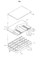
- FIG. 1 is a perspective view illustrating an embodiment of the structure of a plasma display panel according to the present invention.
- the plasma display panel includes a scan electrode 11 and a sustain electrode 12 (that is, a sustain electrode pair), which are formed over an upper substrate 10, and address electrodes 22 formed over a lower substrate 20.
- the sustain electrode pair 11 and 12 includes transparent electrodes 11 a and 12a generally formed of indium-tin-oxide (ITO), and bus electrodes 11 b and 12b.
- the bus electrodes 11 b and 12b may be formed of metal, such as silver (Ag) or chrome (Cr), a stack type of Cr/copper (Cu)/Cr or Cr/aluminum (Al)/Cr.
- the bus electrodes 11 b and 12b are formed on the transparent electrodes 11 a and 12a, and function to decrease a voltage drop caused by the transparent electrodes 11 a and 12a with a high resistance.
- the sustain electrode pair 11 and 12 may have a stack structure of the transparent electrodes 11 a and 12a and the bus electrodes 11 b and 12b, but also include only the bus electrodes 11 b and 12b without the transparent electrodes 11 a and 12a.
- This structure is advantageous in that it can save the manufacturing cost of the plasma display panel because the transparent electrodes 11 a and 12a are not used.
- the bus electrodes 11 b and 12b used in the structure may also be formed using a variety of materials, such as a photosensitive material, other than the above-listed materials.
- Black matrices 15 are arranged between the transparent electrodes 11 a and 12a and the bus electrodes 11 b and 12b of the scan electrode 11 and the sustain electrode 12.
- the black matrix 15 has a light-shielding function of absorbing external light generated outside the upper substrate 10 and decreasing reflection of the light and a function of improving the purity and contrast of the upper substrate 10.
- the black matrices 15 in accordance with an embodiment of the present invention are formed over the upper substrate 10.
- Each black matrix 15 may include a first black matrix 15 formed at a location where it overlaps a barrier rib 21, and second black matrices 11c and 12c formed between the transparent electrodes 11a and 12a and the bus electrodes 11 b and 12b.
- the first black matrix 15, and the second black matrices 11c and 12c which are also referred to as black layers or black electrode layers, may be formed at the same time and, therefore, may be connected to each other physically.
- the first black matrix 15, and the second black matrices 11c and 12c may not be formed at the same time and, therefore, may not be connected to each other physically.
- first black matrix 15 and the second black matrices 11c and 12c are physically connected to each other, the first black matrix 15 and the second black matrices 11c and 12c are formed using the same material. However, in the event that the first black matrix 15 and the second black matrices 11c and 12c are physically separated from each other, they may be formed using different materials.
- the bus electrodes 11 b and 12b or the barrier ribs 21 may have a dark color to perform a light-shielding function of absorbing external light generated outside the upper substrate 10 and decreasing reflection of the light and a function of improving the purity and contrast of the upper substrate 10, like the black matrix.
- a specific member, e.g., an upper dielectric layer 13 formed on the upper substrate 10 and a specific member, e.g., the rib 21 formed on the lower substrate 20 are in a complementary-color relation to each other, so that an overlapped portion of the complementary colors is seen close to black when being seen from a front side of the panel, thereby performing the same function as the black matrix.
- An upper dielectric layer 13 and a protection layer 14 are laminated over the upper substrate 10 on which the scan electrodes 11 and the sustain electrodes 12 are formed in parallel. Charged particles generated by discharge are accumulated on the upper dielectric layer 13.
- the upper dielectric layer 13 and the protection layer 14 may function to protect the sustain electrode pair 11 and 12.
- the protection layer 14 functions to protect the upper dielectric layer 13 from sputtering of charged particles generated at the time of gas discharge and also increase emission efficiency of secondary electrons.
- the address electrodes 22 cross the scan electrodes 11 and the sustain electrodes 12.
- a lower dielectric layer 24 and the barrier ribs 21 are formed over a lower substrate 20 over which the address electrodes 22 are formed.
- Phosphor layers 23 are formed on the surfaces of the lower dielectric layer 24 and the barrier ribs 21.
- Each barrier rib 21 has a longitudinal barrier rib 21 a and a traverse barrier rib 21 b formed in a closed type.
- the barrier rib 21 functions to partition discharge cells physically and prevent ultraviolet rays, which are generated by discharge, and a visible ray from leaking to neighboring discharge cells.
- a filter 100 may be formed on the front side of the plasma display panel according to the present invention.
- the filter 100 may include an external light blocking sheet, an anti-reflection (AR) sheet, a near infrared (NIR) shielding sheet, an electromagnetic interference (EMI) shielding sheet, a diffusion sheet, an optical sheet, and the like.
- AR anti-reflection
- NIR near infrared
- EMI electromagnetic interference
- the gap between the filter 100 and the panel is about 10 ⁇ m to about 30 ⁇ m, light incident from the outside of the panel can be effectively shielded, and light generated from the panel can be effectively emitted to the outside of the panel.
- the gap between the filter 100 and the panel may be about 30 ⁇ m to about 120 ⁇ m.
- An adhesive layer having a function of absorbing impact may be formed between the filter 100 and the panel to prevent impact applied from the outside of the panel.
- the embodiment of the present invention may also be applied to not only the structure of the barrier ribs 21 shown in FIG. 1 , but also various forms of structures of the barrier ribs 21.
- the present embodiment may be applied to a differential type barrier rib structure in which the longitudinal barrier rib 21 a and the traverse barrier rib 21 b have different heights, a channel type barrier rib structure in which a channel, which can be used as an exhaust passage, is formed in at least one of the longitudinal barrier rib 21 a and the traverse barrier rib 21 b, a hollow type barrier rib structure in which a hollow is formed in at least one of the longitudinal barrier rib 21 a and the traverse barrier rib 21 b, and so on.
- the traverse barrier rib 21 b may have a higher height than the longitudinal barrier rib 21a.
- a channel or hollow may be formed in the traverse barrier rib 21 b.
- the red (R), green (G), and blue (B) discharge cells are arranged on the same line.
- the discharge cells may be arranged in different forms.
- the R, G, and B discharge cells may also have a delta type arrangement of a triangle.
- the discharge cells may be arranged in various forms, such as square, pentagon and hexagon.
- the phosphor layer 23 is excited with ultraviolet rays generated during the discharge of a gas, thus generating a visible ray of one of R, G, and B.
- Discharge spaces between the upper/lower substrates 10 and 20 and the barrier ribs 21 are injected with an inert mixed gas for discharge, such as He+Xe, Ne+Xe or He+Ne+Xe.
- FIG. 2 is a sectional view illustrating an embodiment of the schematic sectional structure of an electromagnetic shielding sheet according to the present invention.
- the electromagnetic shielding sheet 110 includes a base sheet 120, a first layer 130 formed on a first surface of the base sheet 120, and a second layer 140 formed on a second surface of the base sheet 120.
- the base sheet 120 may be made of a transparent plastic material, e.g., a resin-based material formed using an ultraviolet (UV) curing method so that light can sufficiently pass therethrough.
- a solid glass material may be used for the base sheet 120.
- the base sheet 120 may include a polyester-based resin such as polyethylene terephthalate and polyethylene naphthalate, a polyamid-based resin such as nylon 6 or nylon 610, a polyolefin-based resin such as polypropylene or polyethylene, a vinyl-based resin such as polyvinyl chloride, an acrylic-based resin such as polyethyl methacrylate or polymethyl methacrylate, an engineering resin such as polyarylate, polysulfone, polyphenylene ether or polyaramide, a styrene-based resin such as polycarbonate or polystyrene, a cellulose-based resin such as triacetylcellulose (TRC), and the like.
- a polyester-based resin such as polyethylene terephthalate and polyethylene naphthalate
- a polyamid-based resin such as nylon 6 or nylon 610
- a polyolefin-based resin such as polypropylene or polyethylene
- a vinyl-based resin such as poly
- the thickness of the base sheet 120 may be about 50 ⁇ m to 200 ⁇ m to improve the luminance of a display image by maintaining the transmittance of the base sheet 120 as 80% or more and prevent the damage of the electromagnetic shielding sheet due to external pressure.
- Electromagnetic waves radiated from the panel to the front have a bad influence on a user's body, and electromagnetic waves radiated from the panel to the rear have an influence on a panel driving circuit, which may cause malfunction.
- the first layer 130 may be an electromagnetic shielding layer that functions to shield electromagnetic waves described above, and the second layer 140 may be an external light blocking layer that functions to absorb external light incident from the outside of the panel.
- the first layer 130 may include a plurality of patterns 150 containing a conductive material. At least some of the plurality of patterns 150 are electrically connected to a ground voltage source and allow electromagnetic waves to be discharged to a ground, so that the electromagnetic waves can be shielded.
- the patterns 150 formed on the first layer 130 are electrically connected to a back cover of the plasma display apparatus, grounded to the ground voltage source, and allows electromagnetic waves to be discharged to the ground, so that the electromagnetic waves can be shielded.
- the plurality of patterns 150 formed on the first layer 130 may include at least one of Cu, Ag, Al, Ni, Pt and carbon nano tube (CNT). Further, the plurality of patterns 150 may be formed in a mesh form.
- the second layer 140 may include a plurality of patterns 160 that absorb external light.
- the patterns 160 formed on the second layer 140 are formed of a material having a darker color than the base sheet 120, e.g. a black material.
- the plurality of patterns 160 include a light absorbing material, e.g., a carbon-based material or are coated with a black dye to maximize the effect of absorbing external light.
- the plurality of patterns 160 formed on the second layer 140 may include light absorbing particles, and the light absorbing particles may be resin particles colored with a certain color.
- the light absorbing particles may be colored with black so as to maximize the light absorption effect.
- the size of the light absorbing particle may be more than 1 ⁇ m so as to facilitate the preparation of the light absorbing particles and injection into the patterns 160 and to maximize the effect of absorbing external light.
- the pattern 160 may include more than 10 wt% light absorbing particles. That is, the light absorbing particles having a weight of more than 10% relative to the total weight of the patterns 160 may be included in the patterns 160.
- an external light source is generally positioned at an upside of the panel, external light may be diagonally incident into the panel from the upside of the panel.
- external light (indicated by solid lines) diagonally incident into the panel is absorbed into a plurality of patterns 240 formed on a second surface of a base sheet 220, and may also be absorbed into a plurality of patterns 230 formed on a first surface of the base sheet 220.
- Panel light (indicated by dotted lines) emitted from a panel 200 for display is radiated to the outside of the panel through portions at which the plurality of patterns 230 and 240 are not formed.
- the patterns 230 may be darkened.
- the pattern 230 may be a metal, a surface of which is darkened.
- an electromagnetic shielding sheet 210 can perform the function of shielding electromagnetic waves and blocking external light. Further, the transmittance of the panel (indicated by the dotted lines) is improved, so that an ambient contrast ratio can be enhanced without lowering the luminance of a display image.
- the distance d between the electromagnetic shielding sheet 210 and the panel 200 may be about 0.02mm to about 5cm so as to improve the transmittance of panel light and prevent the blurring phenomenon of a display image while maximizing the external light blocking effect.
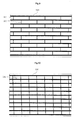
- FIGS. 4 and 5 are views illustrating embodiments of the structure of an electromagnetic shielding layer formed on the first surface of the base sheet 220.
- the electromagnetic shielding layer formed on the first surface of the base sheet 220 may include a plurality of patterns 231 and 232 formed in directions crossing each other.
- the electromagnetic shielding layer may include a plurality of horizontal patterns 231 formed in parallel with a long side of the base sheet 220, and a plurality of vertical patterns 232 formed in parallel with a short side of the base sheet 220.
- the vertical patterns 232 are electrically connected to a ground voltage source and allow electromagnetic waves to be discharged to a ground, so that the electromagnetic waves can be shielded.
- the horizontal patterns 231 function to absorb external light diagonally incident from the upside of the panel.
- FIG. 5 is an enlarged view of a portion indicated by a dotted line in the electromagnetic shielding layer shown in FIG. 4 .
- the width w2 of the vertical pattern 232 for shielding electromagnetic waves may be smaller than the width w1 of the horizontal pattern 231 for blocking external light so as to prevent the luminance of a display image from being lowered due to reduction of the aperture ratio of the electromagnetic shielding sheet and to minimize reduction of the left/right viewing angle of the panel.
- the width w1 of the horizontal pattern 231 and the width w2 of the vertical pattern 232 may be about 100 ⁇ m or less so as to prevent quality of a display image from being degraded due to the exposure of the patterns 231 and 232 formed in the electromagnetic shielding sheet to a user's eyesight.
- the width w1 of the horizontal pattern 231 and the width w2 of the vertical pattern 232 may be about 5 ⁇ m or more.
- a moire phenomenon may occur due to the overlapping of the plurality of patterns 231 and 232 formed in the electromagnetic shielding sheet and a black matrix, a black layer, bus electrodes, barrier ribs and the like, which are formed with a predetermined pattern in the panel.
- the moire phenomenon refers to a low-frequency pattern generated while patterns of similar lattice shapes are overlapped with each other.
- the low-frequency pattern includes a wave pattern seen when mosquito nets overlap each other, and the like.
- the width w1 of the horizontal pattern 231 may be about 30 ⁇ m or less.
- the pitch p2 between adjacent vertical patterns 232 may be greater than the pitch p1 between adjacent horizontal patterns 231.
- a light source (not shown) emitting external light that has an influence on degradation of the ambient contrast ratio by being incident onto the panel is positioned at the upside of the panel and incident onto the panel at an incident angle of about 30 to about 60 degrees.
- the pitch p1 between adjacent horizontal patterns 231 may be about 30 ⁇ m to about 1000 ⁇ m so as to effectively absorb external light incident at an incident angle of about 30 to about 60 degrees as described above and to minimize reduction of the luminance of a display image by securing the transmittance of the electromagnetic shielding sheet.
- the pitch p2 between adjacent horizontal patterns 232 In the event that the pitch p2 between adjacent horizontal patterns 232 is too small, the transmittance of the electromagnetic shielding sheet may be decreased. In the event that the pitch p2 between adjacent horizontal patterns 232 is too large, electromagnetic shielding performance may be lowered. Therefore, the pitch p2 between adjacent horizontal patterns 232 may be in a range of about 30 ⁇ m to about 2000 ⁇ m.
- the electromagnetic shielding layer including the plurality of patterns 231 and 232 shown in FIGS. 4 and 5 may have an aperture ratio of about 50% to about 95%.
- FIGS. 6 and 7 are views illustrating embodiments of the structure of the external light blocking layer formed on the second surface of the base sheet 220.
- the external light blocking layer formed on the second surface of the base sheet 220 may include a plurality of external light absorbing patterns 241 formed in parallel.
- the plurality of external light absorbing patterns 241 may be formed in a direction parallel with the long side of the base sheet 220.
- the external light absorbing patterns 241 absorb external light diagonally incident from the upside of the panel.
- FIG. 7 is an enlarged view of a portion indicated by a dotted line in the external light blocking layer shown in FIG. 6 .
- the width w3 of the external light absorbing pattern 241 may be about 100 ⁇ m or less so as to prevent the external light absorbing patterns 241 formed in the electromagnetic shielding sheet from being exposed to a user's eyesight. However, the width w3 of the external light absorbing pattern 241 may be about 5 ⁇ m or more so as to prevent the function of blocking external light from being lowered.
- the width w3 of the external light absorbing pattern 241 may be about 5 ⁇ m to about 30 ⁇ m.
- the pitch p3 between adjacent external light absorbing patterns 241 may be about 30 ⁇ m to about 1000 ⁇ m so as to enhance external light absorbing efficiency and to minimize reduction of the luminance of a display image by securing the transmittance of the electromagnetic shielding sheet.
- the width w3 of the external light absorbing pattern 241 may be equal to the width w1 of the horizontal pattern 231 and greater than the width w2 of the vertical pattern 232 of the electromagnetic shielding layer.
- the pitch p3 between the external light absorbing patterns 241 may be equal to the pitch p1 between the horizontal patterns 231 and smaller than the pitch p2 between the vertical patterns 232 of the electromagnetic shielding layer.
- the external light blocking layer including the plurality of patterns 241 shown in FIGS. 6 and 7 may have an aperture ratio of about 50% to about 95%.
- the horizontal patterns 231 included in the electromagnetic shielding layer of the electromagnetic shielding sheet and the external light absorbing patterns 241 included in the external light blocking layer of the electromagnetic shielding sheet may have patterns overlapping each other, a moire phenomenon may occur due to the overlapping of the two patterns 231 and 241.
- the external light absorbing patterns included in the external light blocking layer may be diagonally formed with respect to the horizontal patterns 231 included in the electromagnetic shielding layer.
- the aperture ratio of the electromagnetic shielding sheet decreases, and therefore, the luminance of a display image may be lowered.
- the angle ⁇ 1 made between the horizontal pattern 231 and the external light absorbing pattern 241 may be 1.1 to 25 degrees.
- FIGS. 9 and 10 are views illustrating embodiments of the entire form of a plurality of patterns formed in the electromagnetic shielding sheet according to the present invention.
- the positions of vertical patterns 310 and 320 formed in the electromagnetic shielding layer may not be formed to correspond to each other but formed to cross each other.
- the moire phenomenon that occurs due to the overlapping of certain patterns between the vertical patterns and the electrodes formed in the panel may be reduced through the electromagnetic shielding sheet having the entire form shown in FIG. 9 .
- horizontal patterns 330 and vertical patterns 340 formed in the electromagnetic shielding layer are not perpendicular to each other, but the vertical patterns 340 may be diagonally formed.
- the moire phenomenon that occurs due to the overlapping of certain patterns between the vertical patterns and the electrodes or ribs formed in the panel may be reduced through the electromagnetic shielding sheet having the entire form shown in FIG. 10 .
- the angle ⁇ 2 made between the horizontal pattern 330 and the vertical pattern 340 may be 65 to 89 degrees.
- the external light blocking layer of the electromagnetic shielding sheet shown in FIGS. 6 and 7 includes the external light absorbing patterns 241 formed in a direction parallel with the long side of the base sheet
- the external light blocking layer of the electromagnetic shielding sheet according to embodiments of the present invention may include external light absorbing patterns formed in a direction parallel with the short side of the base sheet as shown in FIGS. 4 and 9 or 10 .
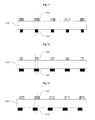
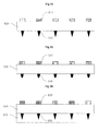
- FIGS. 11 to 17 are sectional views illustrating embodiments of the sectional structure of the electromagnetic shielding sheet according to the present invention.
- horizontal patterns 410 formed on a first surface of a base sheet 400 and external light absorbing patterns 420 formed on a second surface of the base sheet 400 may be formed at positions overlapping each other so that the luminance of a display image is improved by enhancing the aperture ratio of the electromagnetic shielding sheet.
- the horizontal patterns 410 formed on the first surface of the base sheet 400 and the external light absorbing patterns 420 formed on a second surface of the base sheet 400 may partially overlap each other.
- the sectional shape of the external light absorbing pattern formed on the external light blocking layer of the electromagnetic shielding sheet according to the present invention may be various shapes as well as a square shape as described above.
- an external light absorbing pattern 520 formed on the external light blocking layer of the electromagnetic shielding sheet may have a sectional shape of a triangle, e.g., an isosceles triangle.
- an edge portion of the external light absorbing pattern 520 may have a curved sectional shape.
- sectional shape of the external light absorbing pattern formed on the external light blocking layer of the electromagnetic shielding sheet has been described above, the sectional shape of a pattern formed on the electromagnetic shielding layer of the electromagnetic shielding sheet according to the present invention may be various shapes as well as a square shape.
- FIGS. 16 and 17 are views illustrating other embodiments of the sectional structure of the electromagnetic shielding sheet according to the present invention.
- the electromagnetic shielding sheet according to the present invention may include two or more base sheets.
- a first base sheet 600 is laminated on a second base sheet 610.
- a first layer including a plurality of patterns 620 may be formed on the first base sheet 600, and a second layer including a plurality of patterns 630 may be formed between the first and second base sheets 600 and 610.
- the plurality of patterns 630 formed between the first and second base sheets 600 and 610 may be external light absorbing patterns for absorbing external light, and the sectional shape of the plurality of patterns 630 may be various shapes including a square and the like, as well as the a triangle shown in FIG. 16 .
- an electromagnetic shielding sheet may have a structure in which a first base sheet 700 is interposed between a second base sheet 710 and a third base sheet 720.
- a plurality of patterns 730 for shielding electromagnetic waves are formed between the first and second sheets 700 and 710, and a plurality of patterns 740 for absorbing external light are formed between the first and third sheets 700 and 720.
- the plurality of external light absorbing patterns 630 may be formed by forming a plurality of grooves in the second base sheet 610 and then filling a material including a light absorbing material in the plurality of grooves.
- FIG. 18 is a view illustrating an embodiment of the structure of the electromagnetic shielding sheet disposed on the front side of the plasma display panel.
- a moire phenomenon may occur due to the overlapping of the plurality of patterns 810 and 820 formed at predetermined pitches in the electromagnetic shielding sheet and a black matrix, a black layer, bus electrodes, barrier ribs and the like, which are formed with a predetermined pattern in a panel 800.
- the electromagnetic shielding sheet may be diagonally arranged with respect to the panel as shown in FIG. 18 .
- the left/right viewing angle may be extremely decreased, and the ambient contrast ratio of a display image may be lowered.
- the angle ⁇ 3 made between the horizontal pattern 810 and the long side of the panel 800 may be about 0 to about 50 degrees so as to sufficiently secure the left/right viewing angle of the panel, to improve the ambient contrast ratio of a display image, and to reduce the moire phenomenon.
- FIGS. 19 to 23 are sectional views illustrating embodiments of a method of forming the electromagnetic shielding sheet according to the present invention.
- a plurality of electromagnetic shielding patterns 920 for shielding electromagnetic waves are formed on a first base sheet 910, and a plurality of external light blocking patterns 930 for blocking external light are formed on a second base sheet 900.
- the first and second base sheets 910 and 900 may be made of a transparent plastic material through which light can sufficiently pass, e.g., a resin-based material formed using a UV curing method.
- a solid glass material may be used for the first and second base sheets 910 and 900.
- the positions of the electromagnetic shielding patterns 920 and the external light blocking patterns 930 may be changed with each other.
- the external light blocking patterns 930 may be positioned between the first and second base sheets 910 and 900.
- a first base sheet 950 having electromagnetic shielding patterns 960 may have a broader area than a second base sheet 940 having external light blocking patterns 970 to ground electromagnetic shielding patterns positioned at edges of the panel in the electromagnetic shielding patterns 960.
- a filter for display may have a structure in which a plurality of functional layers 1040, 1050 and 1060 are sequentially laminated on a first base 1000.
- the plurality of functional layers 1040, 1050 and 1060 may be an anti-reflection (AR) layer, a near infrared (NIR) shielding layer, an optical layer, respectively.
- AR anti-reflection
- NIR near infrared
- the AR layer prevents light incident from the outside of the panel from being reflected to reduce a dazzling phenomenon, and the NIR shielding layer shields near-infrared light radiated from the panel so that signals transmitted through infrared light used for a remote controller or the like can be normally transmitted.
- the optical layer includes a predetermined dye or pigment, and functions to improve the color temperature and luminance of light radiated from the panel.
- Adhesive layers 1070 are formed between the functional layers 1040 and 1050, between the functional layers 1050 and 1060, and between the first base sheet 1000 and the functional layer 1040 to allow the respective functional layers to be strongly adhered to one another.
- base sheets (not shown) made of a transparent material may be formed between the respective functional layers.
- the laminating order of the plurality of functional layers 1040, 1050, and 1060 may be varied by those skilled in the art. Alternatively, at least any one of the respective functional sheets may be omitted.
- a solid glass material may be used for the first base sheet 1000.
- electromagnetic shielding patterns 1020 may be directly formed on the other surface of the first base sheet 1000 having the plurality of functional layers 1040, 1050 and 1060 formed on one surface of the first base sheet 1000.
- the electromagnetic shielding pattern 1020 may be directly formed on the first base sheet 1000 made of a glass material using an off-set method, a printing method, a plating method or the like.
- external light blocking patterns 1030 may be formed on a second base sheet 1010, and the second base sheet 1010 may be made of a transparent plastic material, e.g., a resin-based material formed using an ultraviolet (UV) curing method so that light can sufficiently pass therethrough.
- a transparent plastic material e.g., a resin-based material formed using an ultraviolet (UV) curing method so that light can sufficiently pass therethrough.
- UV ultraviolet
- the positions of the electromagnetic shielding patterns 1020 and the external light blocking patterns 1030 may be changed with each other.
- the external light blocking patterns 1030 may be directly formed on the first base sheet 1000.
- FIG. 22 is a sectional view illustrating another embodiment of the structure of a plasma display apparatus having an electromagnetic shielding sheet formed on the front side of a plasma display panel according to the present invention. Description of the plasma display panel having the same structure of the plasma display panel described with reference to FIG. 1 will be omitted herein.
- electromagnetic shielding patterns 1120 may be directly formed on an upper substrate 10 having scan and sustain electrodes 11 and 12.
- the electromagnetic shielding pattern 1020 may be directly formed on the upper substrate 10 made of a glass material using an off-set method, a printing method, a plating method or the like.
- a base sheet 1100 is formed on the electromagnetic shielding patterns 1020, and external light blocking patterns 1110 are formed on the base sheet 1100.
- the base sheet 1100 may be made of a transparent plastic material, e.g., a resin-based material formed using an ultraviolet (UV) curing method so that light can sufficiently pass therethrough.
- UV ultraviolet
- a base sheet 1130 of the filter is formed on the external light blocking patterns 1110, and a plurality of functional layers 1140 are laminated on the base sheet 1130 of the filter as described with reference to FIG. 21 .
- the base sheet 1130 of the filter may be made of a transparent plastic material, e.g., a resin-based material formed using an ultraviolet (UV) curing method so that light can sufficiently pass therethrough.
- a solid glass material may be used for the base sheet 1130 of the filter.
- the electromagnetic shielding sheet according to the present invention may be used for various display panels such as a liquid crystal display (LCD), an organic light emitting diode (OLED), a field effect display (FED), a surface-conduction electron-emitter display (SED) and the like.
- LCD liquid crystal display
- OLED organic light emitting diode
- FED field effect display
- SED surface-conduction electron-emitter display
- conductive patterns for shielding electromagnetic waves and blocking external light are formed on a first surface of a base sheet, and patterns for blocking external light are formed on a second surface of the base sheet, so that the functions of shielding electromagnetic waves and blocking external light can be simultaneously performed using one sheet, and therefore, the ambient contrast ratio of a display image can be enhanced without increasing manufacturing costs.
- patterns for shielding electromagnetic waves are directly formed a glass member of a filter or an upper substrate of the panel, so that processes of forming an electromagnetic shielding sheet can be easily performed.
Landscapes
- Engineering & Computer Science (AREA)
- Physics & Mathematics (AREA)
- Plasma & Fusion (AREA)
- Microelectronics & Electronic Packaging (AREA)
- Electromagnetism (AREA)
- Devices For Indicating Variable Information By Combining Individual Elements (AREA)
- Shielding Devices Or Components To Electric Or Magnetic Fields (AREA)
Applications Claiming Priority (2)
| Application Number | Priority Date | Filing Date | Title |
|---|---|---|---|
| KR20070125642 | 2007-12-05 | ||
| KR1020080039431A KR101041937B1 (ko) | 2007-12-05 | 2008-04-28 | 전자파 차폐 시트 및 그를 이용한 플라즈마 디스플레이장치 |
Publications (2)
| Publication Number | Publication Date |
|---|---|
| EP2068341A2 true EP2068341A2 (fr) | 2009-06-10 |
| EP2068341A3 EP2068341A3 (fr) | 2010-06-02 |
Family
ID=39879979
Family Applications (1)
| Application Number | Title | Priority Date | Filing Date |
|---|---|---|---|
| EP08165309A Withdrawn EP2068341A3 (fr) | 2007-12-05 | 2008-09-26 | Feuille de protection électromagnétique et appareil d'affichage plasma l'utilisant |
Country Status (3)
| Country | Link |
|---|---|
| US (1) | US8035039B2 (fr) |
| EP (1) | EP2068341A3 (fr) |
| JP (1) | JP2009139919A (fr) |
Cited By (1)
| Publication number | Priority date | Publication date | Assignee | Title |
|---|---|---|---|---|
| EP2157597A1 (fr) * | 2008-08-19 | 2010-02-24 | Samsung SDI Co., Ltd. | Filtre pour panneau d'affichage à plasma et appareil d'affichage à plasma doté du filtre |
Families Citing this family (13)
| Publication number | Priority date | Publication date | Assignee | Title |
|---|---|---|---|---|
| JP2010165032A (ja) * | 2009-01-13 | 2010-07-29 | Hitachi Displays Ltd | タッチパネルディスプレイ装置 |
| TW201137489A (en) * | 2010-04-28 | 2011-11-01 | Hon Hai Prec Ind Co Ltd | Light blocking member, method for making same and lens module having same |
| US9302452B2 (en) | 2012-03-02 | 2016-04-05 | Ppg Industries Ohio, Inc. | Transparent laminates comprising inkjet printed conductive lines and methods of forming the same |
| US9986669B2 (en) * | 2015-11-25 | 2018-05-29 | Ppg Industries Ohio, Inc. | Transparency including conductive mesh including a closed shape having at least one curved side |
| US11745702B2 (en) | 2018-12-11 | 2023-09-05 | Ppg Industries Ohio, Inc. | Coating including electrically conductive lines directly on electrically conductive layer |
| EP3756076B1 (fr) | 2019-05-10 | 2024-11-27 | Google LLC | Assemblage de capteur préfabriqué pour des objets interactifs |
| USD945293S1 (en) | 2019-08-26 | 2022-03-08 | Google Llc | Sensor assembly |
| US10963106B2 (en) | 2019-08-26 | 2021-03-30 | Google Llc | Pre-fabricated sensor system including removable electronics device |
| USD945295S1 (en) | 2019-08-26 | 2022-03-08 | Google Llc | Sensor system |
| USD945294S1 (en) | 2019-08-26 | 2022-03-08 | Google Llc | Sensor assembly receptacle |
| USD938414S1 (en) | 2019-08-26 | 2021-12-14 | Google Llc | Removable electronics device |
| USD945296S1 (en) | 2019-08-26 | 2022-03-08 | Google Llc | Sensor system receptacle |
| US10908732B1 (en) | 2019-08-26 | 2021-02-02 | Google Llc | Removable electronics device for pre-fabricated sensor assemblies |
Family Cites Families (15)
| Publication number | Priority date | Publication date | Assignee | Title |
|---|---|---|---|---|
| US6262364B1 (en) * | 1997-06-24 | 2001-07-17 | Bridgestone Corporation | Electromagnetic-wave shielding and light transmitting plate |
| KR100322087B1 (ko) * | 1999-04-30 | 2002-02-04 | 김순택 | 외광반사가 저감된 플라즈마 디스플레이 및 그 제조방법 |
| KR100926712B1 (ko) * | 2003-05-28 | 2009-11-17 | 엘지전자 주식회사 | 전면 필터와 그의 제조 방법 |
| KR20060126433A (ko) * | 2003-09-01 | 2006-12-07 | 다이니폰 인사츠 가부시키가이샤 | 플라즈마 디스플레이용 전자파 차폐 필름 |
| KR100565494B1 (ko) | 2003-09-17 | 2006-03-30 | 엘지전자 주식회사 | 플라즈마 디스플레이 패널의 구조 |
| KR20050110773A (ko) | 2004-05-19 | 2005-11-24 | 삼성코닝 주식회사 | Pdp 필터, 이를 포함한 pdp 장치 및 pdp 필터의제조방법 |
| KR100780283B1 (ko) | 2004-09-01 | 2007-11-28 | 삼성코닝 주식회사 | 전자파 차폐 필름 및 이의 제조방법 |
| KR100769900B1 (ko) * | 2005-07-21 | 2007-10-24 | 엘지전자 주식회사 | 필름형 전면필터 및 이를 이용한 플라즈마 디스플레이 패널모듈 |
| US7755263B2 (en) * | 2005-05-04 | 2010-07-13 | Samsung Corning Precision Glass Co., Ltd. | External light-shielding layer, filter for display device including the external light-shielding layer and display device including the filter |
| KR20070037329A (ko) | 2006-09-22 | 2007-04-04 | 엘지전자 주식회사 | 플라즈마 디스플레이 장치 |
| EP1770750A3 (fr) * | 2005-09-30 | 2009-03-11 | Lg Electronics Inc. | Ecran plasma |
| KR100852858B1 (ko) * | 2006-02-07 | 2008-08-18 | 주식회사 엘지화학 | 전자파차폐필름 및 이를 포함하는 광학필터 |
| KR100746255B1 (ko) * | 2006-03-13 | 2007-08-03 | 엘지전자 주식회사 | 온 사이트형 pdp 전면 필터의 제조 방법 및 이에 의해제조된 전면 필터를 포함하는 플라즈마 디스플레이 패널 |
| KR100761298B1 (ko) * | 2006-09-08 | 2007-09-27 | 엘지전자 주식회사 | 플라즈마 디스플레이 장치 |
| US8125147B2 (en) * | 2006-07-19 | 2012-02-28 | Lg Electronics Inc. | Plasma display device with light-absorbing filter |
-
2008
- 2008-07-09 JP JP2008178754A patent/JP2009139919A/ja not_active Withdrawn
- 2008-09-26 EP EP08165309A patent/EP2068341A3/fr not_active Withdrawn
- 2008-09-29 US US12/240,831 patent/US8035039B2/en not_active Expired - Fee Related
Cited By (1)
| Publication number | Priority date | Publication date | Assignee | Title |
|---|---|---|---|---|
| EP2157597A1 (fr) * | 2008-08-19 | 2010-02-24 | Samsung SDI Co., Ltd. | Filtre pour panneau d'affichage à plasma et appareil d'affichage à plasma doté du filtre |
Also Published As
| Publication number | Publication date |
|---|---|
| US8035039B2 (en) | 2011-10-11 |
| EP2068341A3 (fr) | 2010-06-02 |
| JP2009139919A (ja) | 2009-06-25 |
| US20090145654A1 (en) | 2009-06-11 |
Similar Documents
| Publication | Publication Date | Title |
|---|---|---|
| US8035039B2 (en) | Electromagnetic shielding sheet, plasma display apparatus using the same, and related technology | |
| US7764016B2 (en) | Plasma display device | |
| KR20080041540A (ko) | 필터 및 그를 이용한 플라즈마 디스플레이 장치 | |
| US8013807B2 (en) | Plasma display device | |
| KR20090016971A (ko) | 플라즈마 디스플레이 장치 | |
| KR100829502B1 (ko) | 필터 및 그를 이용한 플라즈마 디스플레이 장치 | |
| US7710036B2 (en) | Filter and plasma display device | |
| KR101082560B1 (ko) | 디스플레이 필터, 이를 구비한 디스플레이 장치 및 이의 제조방법 | |
| EP1990825A2 (fr) | Feuille de protection externe contre la lumière et dispositif de panneau d'affichage plasma l'utilisant | |
| US8125147B2 (en) | Plasma display device with light-absorbing filter | |
| KR101041937B1 (ko) | 전자파 차폐 시트 및 그를 이용한 플라즈마 디스플레이장치 | |
| KR100912940B1 (ko) | 외광 차단 시트의 제조 방법, 그를 이용한 외광 차단 시트및 디스플레이 장치 | |
| US20110198980A1 (en) | Plasma display apparatus | |
| EP1788611A2 (fr) | Filtre pour appareil d'affichage et appareil d'affichage à plasma avec un tel | |
| KR100809037B1 (ko) | 외광 차단 시트 및 그를 이용한 플라즈마 디스플레이 장치 | |
| US8334653B2 (en) | Filter, plasma display device thereof, and related technologies | |
| KR100783645B1 (ko) | 플라즈마 디스플레이 장치 | |
| KR100848287B1 (ko) | 외광 차단 시트 및 그를 이용한 플라즈마 디스플레이 장치 | |
| KR100883584B1 (ko) | 필터 및 그를 이용한 플라즈마 디스플레이 장치 | |
| KR20080104587A (ko) | 필터 및 그를 이용한 플라즈마 디스플레이 장치 | |
| WO2008010622A1 (fr) | Dispositif d'écran plasma | |
| KR100809622B1 (ko) | 필터 및 그를 이용한 플라즈마 디스플레이 장치 | |
| KR100849425B1 (ko) | 필터 및 그를 이용한 플라즈마 디스플레이 장치 | |
| KR100838599B1 (ko) | 플라즈마 디스플레이 장치 | |
| KR100809039B1 (ko) | 필터 및 그를 이용한 플라즈마 디스플레이 장치 |
Legal Events
| Date | Code | Title | Description |
|---|---|---|---|
| PUAI | Public reference made under article 153(3) epc to a published international application that has entered the european phase |
Free format text: ORIGINAL CODE: 0009012 |
|
| AK | Designated contracting states |
Kind code of ref document: A2 Designated state(s): AT BE BG CH CY CZ DE DK EE ES FI FR GB GR HR HU IE IS IT LI LT LU LV MC MT NL NO PL PT RO SE SI SK TR |
|
| AX | Request for extension of the european patent |
Extension state: AL BA MK RS |
|
| PUAL | Search report despatched |
Free format text: ORIGINAL CODE: 0009013 |
|
| RIC1 | Information provided on ipc code assigned before grant |
Ipc: H05K 9/00 20060101ALI20100421BHEP Ipc: H01J 17/49 20060101ALI20100421BHEP Ipc: H01J 17/16 20060101AFI20081104BHEP |
|
| AK | Designated contracting states |
Kind code of ref document: A3 Designated state(s): AT BE BG CH CY CZ DE DK EE ES FI FR GB GR HR HU IE IS IT LI LT LU LV MC MT NL NO PL PT RO SE SI SK TR |
|
| AX | Request for extension of the european patent |
Extension state: AL BA MK RS |
|
| STAA | Information on the status of an ep patent application or granted ep patent |
Free format text: STATUS: THE APPLICATION IS DEEMED TO BE WITHDRAWN |
|
| 18D | Application deemed to be withdrawn |
Effective date: 20101203 |