EP2068363A2 - MISFET mit Graben-Gate - Google Patents
MISFET mit Graben-Gate Download PDFInfo
- Publication number
- EP2068363A2 EP2068363A2 EP08170802A EP08170802A EP2068363A2 EP 2068363 A2 EP2068363 A2 EP 2068363A2 EP 08170802 A EP08170802 A EP 08170802A EP 08170802 A EP08170802 A EP 08170802A EP 2068363 A2 EP2068363 A2 EP 2068363A2
- Authority
- EP
- European Patent Office
- Prior art keywords
- trench
- layer
- semiconductor
- well
- type
- Prior art date
- Legal status (The legal status is an assumption and is not a legal conclusion. Google has not performed a legal analysis and makes no representation as to the accuracy of the status listed.)
- Ceased
Links
- 239000004065 semiconductor Substances 0.000 claims abstract description 72
- 229910010271 silicon carbide Inorganic materials 0.000 claims abstract description 39
- HBMJWWWQQXIZIP-UHFFFAOYSA-N silicon carbide Chemical compound [Si+]#[C-] HBMJWWWQQXIZIP-UHFFFAOYSA-N 0.000 claims abstract description 36
- 230000007480 spreading Effects 0.000 claims abstract description 9
- 238000003892 spreading Methods 0.000 claims abstract description 9
- 239000013078 crystal Substances 0.000 claims description 13
- 239000000758 substrate Substances 0.000 claims description 9
- 230000005669 field effect Effects 0.000 claims description 5
- 230000000903 blocking effect Effects 0.000 abstract description 15
- 230000000694 effects Effects 0.000 abstract description 7
- 108091006146 Channels Proteins 0.000 description 71
- 238000000034 method Methods 0.000 description 20
- 230000005684 electric field Effects 0.000 description 13
- 238000009826 distribution Methods 0.000 description 10
- 230000002441 reversible effect Effects 0.000 description 8
- 238000013461 design Methods 0.000 description 7
- 238000005530 etching Methods 0.000 description 7
- 241001354791 Baliga Species 0.000 description 5
- VYPSYNLAJGMNEJ-UHFFFAOYSA-N Silicium dioxide Chemical compound O=[Si]=O VYPSYNLAJGMNEJ-UHFFFAOYSA-N 0.000 description 4
- 230000006872 improvement Effects 0.000 description 4
- 230000008569 process Effects 0.000 description 4
- XUIMIQQOPSSXEZ-UHFFFAOYSA-N Silicon Chemical group [Si] XUIMIQQOPSSXEZ-UHFFFAOYSA-N 0.000 description 3
- 238000013459 approach Methods 0.000 description 3
- 238000005468 ion implantation Methods 0.000 description 3
- 238000004519 manufacturing process Methods 0.000 description 3
- 229910044991 metal oxide Inorganic materials 0.000 description 3
- 150000004706 metal oxides Chemical class 0.000 description 3
- OKTJSMMVPCPJKN-UHFFFAOYSA-N Carbon Chemical compound [C] OKTJSMMVPCPJKN-UHFFFAOYSA-N 0.000 description 2
- 230000008901 benefit Effects 0.000 description 2
- 229910052799 carbon Inorganic materials 0.000 description 2
- 238000005516 engineering process Methods 0.000 description 2
- 238000009413 insulation Methods 0.000 description 2
- 239000000463 material Substances 0.000 description 2
- 238000001020 plasma etching Methods 0.000 description 2
- 230000002829 reductive effect Effects 0.000 description 2
- 238000011160 research Methods 0.000 description 2
- 230000004044 response Effects 0.000 description 2
- 229910052710 silicon Inorganic materials 0.000 description 2
- 239000010703 silicon Substances 0.000 description 2
- 235000012239 silicon dioxide Nutrition 0.000 description 2
- 239000000377 silicon dioxide Substances 0.000 description 2
- 239000013598 vector Substances 0.000 description 2
- 101100207343 Antirrhinum majus 1e20 gene Proteins 0.000 description 1
- 108090000699 N-Type Calcium Channels Proteins 0.000 description 1
- 102000004129 N-Type Calcium Channels Human genes 0.000 description 1
- 108010075750 P-Type Calcium Channels Proteins 0.000 description 1
- 125000004432 carbon atom Chemical group C* 0.000 description 1
- 230000015556 catabolic process Effects 0.000 description 1
- 230000003247 decreasing effect Effects 0.000 description 1
- 238000011161 development Methods 0.000 description 1
- 239000002019 doping agent Substances 0.000 description 1
- 239000007943 implant Substances 0.000 description 1
- 230000002401 inhibitory effect Effects 0.000 description 1
- 238000012986 modification Methods 0.000 description 1
- 230000004048 modification Effects 0.000 description 1
- 150000004767 nitrides Chemical class 0.000 description 1
- 238000004886 process control Methods 0.000 description 1
- 230000002459 sustained effect Effects 0.000 description 1
Images


Classifications
-
- H—ELECTRICITY
- H10—SEMICONDUCTOR DEVICES; ELECTRIC SOLID-STATE DEVICES NOT OTHERWISE PROVIDED FOR
- H10D—INORGANIC ELECTRIC SEMICONDUCTOR DEVICES
- H10D30/00—Field-effect transistors [FET]
- H10D30/60—Insulated-gate field-effect transistors [IGFET]
- H10D30/64—Double-diffused metal-oxide semiconductor [DMOS] FETs
- H10D30/66—Vertical DMOS [VDMOS] FETs
- H10D30/668—Vertical DMOS [VDMOS] FETs having trench gate electrodes, e.g. UMOS transistors
-
- H—ELECTRICITY
- H10—SEMICONDUCTOR DEVICES; ELECTRIC SOLID-STATE DEVICES NOT OTHERWISE PROVIDED FOR
- H10D—INORGANIC ELECTRIC SEMICONDUCTOR DEVICES
- H10D18/00—Thyristors
- H10D18/40—Thyristors with turn-on by field effect
-
- H—ELECTRICITY
- H10—SEMICONDUCTOR DEVICES; ELECTRIC SOLID-STATE DEVICES NOT OTHERWISE PROVIDED FOR
- H10D—INORGANIC ELECTRIC SEMICONDUCTOR DEVICES
- H10D30/00—Field-effect transistors [FET]
- H10D30/60—Insulated-gate field-effect transistors [IGFET]
- H10D30/63—Vertical IGFETs
- H10D30/635—Vertical IGFETs having no inversion channels, e.g. vertical accumulation channel FETs [ACCUFET] or normally-on vertical IGFETs
-
- H—ELECTRICITY
- H10—SEMICONDUCTOR DEVICES; ELECTRIC SOLID-STATE DEVICES NOT OTHERWISE PROVIDED FOR
- H10D—INORGANIC ELECTRIC SEMICONDUCTOR DEVICES
- H10D62/00—Semiconductor bodies, or regions thereof, of devices having potential barriers
- H10D62/10—Shapes, relative sizes or dispositions of the regions of the semiconductor bodies; Shapes of the semiconductor bodies
- H10D62/102—Constructional design considerations for preventing surface leakage or controlling electric field concentration
- H10D62/103—Constructional design considerations for preventing surface leakage or controlling electric field concentration for increasing or controlling the breakdown voltage of reverse-biased devices
- H10D62/105—Constructional design considerations for preventing surface leakage or controlling electric field concentration for increasing or controlling the breakdown voltage of reverse-biased devices by having particular doping profiles, shapes or arrangements of PN junctions; by having supplementary regions, e.g. junction termination extension [JTE]
-
- H—ELECTRICITY
- H10—SEMICONDUCTOR DEVICES; ELECTRIC SOLID-STATE DEVICES NOT OTHERWISE PROVIDED FOR
- H10D—INORGANIC ELECTRIC SEMICONDUCTOR DEVICES
- H10D62/00—Semiconductor bodies, or regions thereof, of devices having potential barriers
- H10D62/10—Shapes, relative sizes or dispositions of the regions of the semiconductor bodies; Shapes of the semiconductor bodies
- H10D62/13—Semiconductor regions connected to electrodes carrying current to be rectified, amplified or switched, e.g. source or drain regions
- H10D62/149—Source or drain regions of field-effect devices
- H10D62/151—Source or drain regions of field-effect devices of IGFETs
- H10D62/156—Drain regions of DMOS transistors
- H10D62/157—Impurity concentrations or distributions
-
- H—ELECTRICITY
- H10—SEMICONDUCTOR DEVICES; ELECTRIC SOLID-STATE DEVICES NOT OTHERWISE PROVIDED FOR
- H10D—INORGANIC ELECTRIC SEMICONDUCTOR DEVICES
- H10D62/00—Semiconductor bodies, or regions thereof, of devices having potential barriers
- H10D62/10—Shapes, relative sizes or dispositions of the regions of the semiconductor bodies; Shapes of the semiconductor bodies
- H10D62/17—Semiconductor regions connected to electrodes not carrying current to be rectified, amplified or switched, e.g. channel regions
- H10D62/393—Body regions of DMOS transistors or IGBTs
-
- H—ELECTRICITY
- H10—SEMICONDUCTOR DEVICES; ELECTRIC SOLID-STATE DEVICES NOT OTHERWISE PROVIDED FOR
- H10D—INORGANIC ELECTRIC SEMICONDUCTOR DEVICES
- H10D62/00—Semiconductor bodies, or regions thereof, of devices having potential barriers
- H10D62/40—Crystalline structures
- H10D62/405—Orientations of crystalline planes
-
- H—ELECTRICITY
- H10—SEMICONDUCTOR DEVICES; ELECTRIC SOLID-STATE DEVICES NOT OTHERWISE PROVIDED FOR
- H10D—INORGANIC ELECTRIC SEMICONDUCTOR DEVICES
- H10D62/00—Semiconductor bodies, or regions thereof, of devices having potential barriers
- H10D62/80—Semiconductor bodies, or regions thereof, of devices having potential barriers characterised by the materials
- H10D62/83—Semiconductor bodies, or regions thereof, of devices having potential barriers characterised by the materials being Group IV materials, e.g. B-doped Si or undoped Ge
- H10D62/832—Semiconductor bodies, or regions thereof, of devices having potential barriers characterised by the materials being Group IV materials, e.g. B-doped Si or undoped Ge being Group IV materials comprising two or more elements, e.g. SiGe
- H10D62/8325—Silicon carbide
Definitions
- the invention relates to transistor structures, particularly useful in MOSFETs, in which the conductive channel is formed on the A-face of the semiconductor body.
- the problems addressed by this invention include (i) reducing channel resistance in the on-state for optimal current output and (ii) minimizing field crowding effects to maximize the reverse voltage blocking capabilities within the device.
- transistor designs have been optimized to achieve a controlled current flow in the on-state while simultaneously having the ability to block certain voltages in the off-state.
- semiconductor materials including silicon carbide and the Group III nitrides, has led to extraordinary advancements in transistor design that allow greater control over transistor performance in both the on-state (e.g., higher current output) and the off-state (higher voltage blocking with less leakage current).
- Silicon carbide has been of particular interest due to its electrical characteristics in a variety of crystal structures
- Silicon carbide's crystal structure is often described by the elemental configuration of the layer being used.
- a cross section of a silicon carbide substrate shows either a layer of carbon atoms directly on top of a layer of silicon atoms, or vice versa.
- the silicon layer is often polished and used for forming devices thereon, and it is known as the silicon face. If the carbon layer is exposed, it is known as the carbon face. See Zetterling, Carl-Mikael, Process Technology for Silicon Carbide Devices, Institute of Electrical Engineers (2002), Page 3 .
- the axes of alignment for the silicon carbide crystal also play important roles in choosing the orientation for forming a semiconductor device.
- Traditionally for hexagonal crystal structures, four principal axes are commonly used: a1, a2, a3, and c. All of the a-vectors are in the same plane (“the a-plane), and the c-vector is in the c-plane that is perpendicular to the a-plane
- Yano et al. formed two types of MOSFETs with currents perpendicular to one another on the same substrate. Drain current for the MOSFET formed on the (1120) face improved substantially, showing a significant increase in channel mobility by using the a-face (1120) of the silicon carbide. Yano's design, however, is not preferable in vertical power devices because the Yano devices have a lower critical field and conduct under reversed bias at lower gate voltages than desired. The sole technique of developing the MOSFET on the a-face, without additional parameters being adjusted as well, has not proven to be the best answer in the context of optimizing performance in power MOSFETs
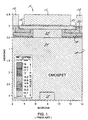
- FIGS 1 and 4 show a prior art DMOSFET (5) and a prior art UMOSFET (28) respectively.
- a traditional DMOSFET (5) includes source, gate, and drain contacts (10, 11, 12) positioned on a semiconductor body (18) with the gate contact (11) atop an oxide layer (15) insulating the gate region.
- the DMOSFET (5) includes a p+ type well (19) implanted into the semiconductor to a depth of about 0.5 microns and doped to about 1 e20 cm -3 .
- An n+ source region (20) doped to about 1e20 cm -3 is adjacent the p+ well (19) and positioned between the p+ well (19) and the buried channel (21).
- the buried channel (21) extends across portions of the source (20), the p+ well (19) and the semiconductor body (18) between active regions, i.e., the JFET region (23).
- the buried channel (21), the JFET region (23), and the supporting drift region (24) of the DMOSFET (5) are doped to about 1e16cm -3 .
- the fabrication process controls the channel surface by using ion implantation instead of doping during layer growth. Ion implantation is difficult to achieve accurately in DMOSFETs, and the resulting devices are limited in channel mobility.
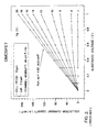
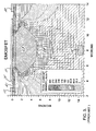
- the channel resistance of the DMOSFET (5) of Figure 1 is set forth in the forward voltage v. current curves of Figure 2 .
- the DMOSFET (5) of Figure 1 achieves channel mobility of 40cm 2 /Vs and a specific on resistance of about 4.62 m ⁇ cm 2 .
- Figure 3 shows the forward current distribution of the prior art DMOSFET (5) of Figure 1 . These values are in line with known DMOSFETs that achieve a typical channel mobility of between about 25 to 50 cm 2 /Vs.
- the current distribution in the drift region (24) of the device is far less than the optimal current in the upper portion (23) closer to the gate.
- Figure 3 shows that the current is not spreading as desired for maximum flow through the device to the drain (12).
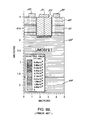
- UMOSFET (28) of Figure 4 suffers similar current restrictions.
- UMOSFET (28) includes the standard source (30), gate (31), and drain (32) with the gate (31) atop an oxide layer (33) lining a trench (36).
- the buried channel (38) of the UMOSFET (28) extends across the source (30) and down into the trench (36) such that the buried channel (38) is between the epitaxial layers of the p-n junction (40, 41) and the oxide layer (33).
- the problem with the prior art UMOSFET is that the corner of the trench (42) exhibits a noted crowding of the electric field at the corner of the trench, inhibiting current flow through the drift region (43) and the substrate (44) down to the drain (32). The field crowding also results in a lower sustained gate voltage during reverse bias operation
- the UMOSFET of Figure 4 also requires a trench that is greater than 2 microns for proper gate placement and operation.
- reactive ion etching is often the method of choice for forming a trench in a UMOSFET, the trench wall is so severely damaged in the fabrication process that the conductive channel is constricted. Uniform results are difficult to achieve when subjecting silicon carbide to reactive ion etching, and the resulting devices are not reliable. The damage caused by the etching also deteriorates the oxide quality formed thereon for insulation purposes.
- U.S. Patent No. 5,976,936 shows another example of a prior silicon carbide MOSFET developed with the goal of increasing current in the channel while controlling the threshold voltage and blocking characteristics for the device.
- the Miyajima '936 patent utilizes a vertical layer of silicon carbide along the gate trench wall for the channel layer.
- the vertical channel layer is quite thin-about 1000 to 5000 angstroms.
- the Miyajima '936 design however, still suffers the problem of current crowding at the edges of the trench.
- Miyajima furthermore, makes no reference to using the a-face of the silicon carbide crystal to enhance channel mobility.
- the invention is a new transistor structure (50) that optimizes current along the A-face of a silicon carbide body (65) while minimizing the JFET effect in the drift region (55) during forward conduction in the on state.
- the invention further shows high voltage blocking ability due to the addition of a highly doped well region (77) that protects the gate corner region (80) in trench-gated device.
- transistors For transistor devices utilizing an etched trench (56) in a semiconductor body for the gate contact (61), conduction along the trench sidewall can be enhanced by providing a conductive path (72) across the A-face of the semiconductor, preferably silicon carbide.
- transistors advantageously use the A-face conduction along a trench sidewall in addition to a buried channel layer (72) extending across portions of the semiconductor mesas (65) defining the trench (56).
- a doped well (77) extends from at least one of the mesas to a depth within the current spreading layer, or drift region (55) that is greater than the depth of the trench (56).
- the current spreading drift layer (55) extends between the semiconductor mesas (65) beneath the bottom of the trench (56) to reduce junction resistance in the on-state.
- semiconductor mesas (65) define a trench (56) there between, and each mesa (65) defines the width of a p-n junction in a respective mesa.
- a buried channel layer (72) is adjacent the top surface of the device, forming an AMOSFET (50) that utilizes conduction along the A-face of silicon carbide.
- the buried channel layer (72) extends down and across the trench wall.
- a deep well region (77), doped, for example, to P+ conductivity, extends from the top of the AMOSFET (50) down to a depth that is greater than the trench (56).
- the deep P+ well (77) protects the trench corner (80) during reverse bias operation, and allows the device to achieve higher blocking voltages.
- a doped buffer layer (73) extends across the body of the device from each vertical trench wall toward the deep well region.
- the invention utilizes the A-face of silicon carbide to control conduction via a gate contact (61).
- the A-face of the silicon carbide enhances channel conductivity by increasing transconductance across the semiconductor.
- a deep well region (77) proximate a buffer region (73) of opposite conductivity type protects the trench corner (80) during reverse bias operation, thereby allowing the device to withstand higher gate blocking voltages.
- the method of forming an AMOSFET according to the invention herein includes implanting a doped well region (77) of a first conductivity type in a semiconductor body (65) and then growing a first epitaxial layer (68) of the first conductivity type on the semiconductor body such that the first epitaxial layer (68) covers at least a portion of the doped well region (77).
- the invention includes forming a pn junction by growing a second epitaxial layer (69) of a second conductivity type on the first epitaxial layer (68) and then etching the epitaxial layers and said semiconductor body to form a pair of mesas.
- the mesas define a trench (56) there between, wherein the trench has a depth into the semiconductor body that is less than the depth of said doped well region (77).
- the channel layer may be formed of silicon carbide and the a-face of the silicon carbide provides the conductive path from source to drain. Also, an N+ type buffer layer may be grown on the semiconductor body prior to the etching step and then etching all of the epitaxial layers and a portion of the underlying semiconductor body.
- the method instead of growing the epitaxial layers (68, 69) individually, the method encompasses the converting of an upper region of said first epitaxial layer to a second conductivity type including by ion implantation.
- the MOSFET of this invention includes a conductive channel on the A-face of a silicon carbide crystal epitaxial layer for increased channel mobility (e.g., up to 200 cm 2 /Vs for the AMOSFET vs. 100 cm 2 /Vs or less for prior art DMOSFETs).
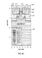
- Figure 5 sets forth the structure of the new AMOSFET (50).
- the drift region (55), or current spreading layer supports epitaxial layers forming the active region of the AMOSFET (50) with current flowing from a source region (60) through the drift region (55), to the drain (62).
- the AMOSFET (50) is a transistor having an insulated gate (61), or control contact, within a trench (56) in a semiconductor crystal structure (58).
- the trench (56) defines a pair of semiconductor mesas (65) that each encompass a p+ type layer (68) and an n+ type layer (69) forming a pn junction therein.
- the p+ type layer (68) is an epitaxial layer positioned under a buried channel (72) and between the trench (56) and a p+ doped well (77).
- the n+ type layer (69) is the source region for conduction purposes.
- the n+ layer (69) is located adjacent the top of p+ layer (68) and beneath the buried channel (72).
- the drift region (55) supports the above-noted active regions of the AMOSFET.
- the drift region (55) is an N+ epitaxial layer on a substrate and extends between the bottom of the trench and a surface of the AMOSFET opposite the gate contact.
- the AMOSFET may include more advanced doping techniques such as utilizing a doping concentration in the drift region (55) that increases from a bottom MOSFET surface proximate the drain (62) toward an upper MOSFET surface proximate the source region (69).
- the most highly doped region of the drift layer is adjacent said P+ well (77)
- the drain contact (62) is affixed to the bottom of the device, allowing conduction from source to drain across the drift region (55). This conduction is controlled by a voltage on the gate (61) in the trench (56). A positive voltage on the gate, above a certain specified threshold, allows controlled conduction from source to drain so long as the channel region (72) is of the proper resistance and channel length.
- An AMOSFET according to this invention includes functional transistor features including source, gate, and drain contacts (60, 61, 62) with the gate contact (61) formed atop an insulating oxide layer (64) within the trench (56).
- the source contact (60) is located on a first surface of the AMOSFET (50) and extends across upper portions of the p+ doped well (77) and the n+ source region (69).
- a buffer layer (73) extends from the p+ well region (77) toward the bottom of the trench (56) with the oxide layer (64) and gate contact (61) inside the trench (56). With the buffer layer (73) properly positioned adjacent the trench corner (80), the p-n junctions between the p+ epitaxial layer (68), the n type buffer layer (73) and the p+ type doped well (77) are sufficiently doped to merge, thereby protecting the trench corner in the off, or non-conductive state. This allows the AMOSFET (50) to withstand higher voltages on the gate (61) without leakage currents toward the drain (62) or even full device breakdown.
- the N+ type buffer layer (73) extends to a depth that is approximately equal to the depth of the buried channel layer (72).
- the doping in each layer is sufficient to provide optimal current in the on-state controlled by a gate (61) having a wide range of voltage levels thereon.
- a gate (61) having a wide range of voltage levels thereon.
- the p+ epitaxial layer (68) is doped to about 5e17cm -3
- the n+ source region is doped to about 1 e20cm -3 .
- the AMOSFET (50) of this invention has a channel layer (72) that is particularly suited for providing high current throughput from source (60) to drain (62), depending on the gate (61) voltage.
- the buried channel layer (72) extends across portions of the top surface of the semiconductor mesas (65) and at least partially covers the outer walls of the trench (56), including the bottom wall, such that the buried channel layer (72) provides a conductive path across the A-face, the 1120 face, of the semiconductor crystal structure forming epitaxial p-n junction layers (68, 69).
- the drift, or current spreading layer (55) extends between the semiconductor mesas (65) beneath the bottom of the trench (56) to reduce the junction field effect resistance in the device.
- the drift layer (55) extends across the width of the semiconductor mesas (65) and the gate trench (61).
- the drift layer (55) may rest on a semiconductor substrate to which the drain contact (62) is attached.
- At least one doped well (77) extends within at least one of the mesas (65) to a depth within the drift region (55) that is greater than the depth of the trench (56).
- the doping levels of the device in Figure 5 are illustrated by the shading in the drawing. While the AMOSFET of this invention is not limited to any particular doping level for any one region, the doping ranges do affect performance, particularly current flow from source to drain.
- the doped well (77) is a p+ type well with a doping level of about 1 e19cm -3 .
- the n+ source region (69) is doped to about 1e20cm -3
- the p+ epitaxial layer (68) is doped to about 5e17cm -3 .
- the buried channel layer (72) has a doping level of about 2e16cm -3 ; the n+ buffer layer is at about 1e16cm -3 , and the drift layer is doped to about 5e15cm -3 .
- the n+ source region (69) and the p+ epitaxial layer are at approximately the same fixed potential.
- the AMOSFET defines a trench between semiconductor mesas such that the trench exposes the A-face (1120) of the semiconductor body.
- Each mesa includes a pn junction for controlling current flow from the source to the drain.
- the mesas (65) have a first semiconductor epitaxial layer (68) of a first conductivity type (e.g., P+) extending across the mesa and abutting the trench (56).
- the mesa (65) includes a second semiconductor epitaxial layer (69) of a second conductivity type (e.g. N+) on the first semiconductor epilayer (68).
- the N+ layer (69) is the source region.
- the buried channel (72) extends from the top of one mesa (65), from an area under at least a portion of the source contact (60), down the trench wall along the A-face of the semiconductor, across the trench bottom, up the opposite wall of the trench, and across the surface of the second mesa (65).
- the buried channel layer (72) extends from the N+ source region of one mesa to the N+ source region of the opposite mesa, thereby covering the trench walls.
- the buried channel (72) is then positioned in proximity to the gate contact (61) with an insulating layer (e.g., silicon dioxide) (64) between the gate contact (61) and the buried channel (72).
- an insulating layer e.g., silicon dioxide
- the buried channel (72) is between the source region of each mesa and the insulating layer under the gate contact.
- the AMOSFET (50) controls electrical conduction in the buried channel (72) along the A-face of the semiconductor body.
- the AMOSFET includes a well region (77) have the first conductivity type (e.g. P+) extending from the first epitaxial layer (68) down into the semiconductor mesa body.
- the AMOSFET (50) of this invention further utilizes a buffer layer (73) having the same conductivity type as the source region (60) (e.g., N+) and extending across at least a portion of the bottom region within each mesa (65), between the trench (56) wall and the well (77).
- the buffer layer (73) forms a pn junction with the well region (77) of the AMOSFET (50) for further conduction control.
- the buffer layer (73) extends from the outer wall of the buried channel (72) to an outer wall of the well (77).
- One advantage of utilizing the A-face (1120) of a silicon carbide crystal structure according to this invention is that of achieving desired performance with a shallower gate trench than that of the prior art.
- Prior art trenches in UMOSFETs exceed 2 microns.
- the gate trench (56) is less than about 2 microns deep, and in a preferred embodiment, the gate trench (56) is less than about 1 micron deep.
- a more preferred embodiment utilizes a gate trench (56) of about 0.8 microns deep.
- the depth of the P+ well (77) is another characteristic of the AMOSFET of Figure 5 .
- the well (77) extends to a depth greater than the buffer layer (73) and even deeper than either the trench (56) or the buried channel (72).
- the deep P+ well (77) protects the trench corner (80) by shielding the field generated by the gate-semiconductor junction.
- the P+ well (77) is approximately 1.3 microns deep, as shown in Figure 5 .
- the forward current distribution is greatly enhanced across a larger section of the drift region (55) due to the additional depth of the P+ well (77) and the use of the buffer layer (73) as shown in Figure 5 . It is significant that the current density distribution approaches 300 A/cm2 over a predominant portion of the AMOSFET of Figure 6 , particularly in the drift region (55).
- the DMOSFET of Figure 3 achieves a current density in the 300 A/cm2 range within a significantly smaller region of the drift region. Most of the drift region of the DMOSFET tested in Figure 3 achieved a current density in the range of 200 - 225 A/cm2.
- Figure 7 illustrates the current output for various gate voltages applied to the AMOSFET device of Figure 5 .
- the specific on resistance of 2.84 mohms ⁇ cm 2 is a significant improvement over the on resistance of 4.62 for the prior art DMOSFET as shown in Figure 2 .
- Using the silicon carbide A-face in the AMOSFET according to this invention results in significant diminution of the resistance in the channel.
- the AMOSFET described herein has a lower on-resistance due to a high channel mobility, a short channel length, a reduced JFET resistance within the semiconductor body, and a high channel density.
- the high channel mobility exhibits a higher transconductance through the buried channel (72) along the A-face (1120). Reducing channel crowding aids in achieving higher current throughput along the A-face.
- These qualities are achieved in a fabrication process that includes a shallow trench etching down to less than about one micron.
- Other embodiments of the invention utilize a trench depth between about 1 micron and 2 microns, which is significantly smaller than trench depths of prior art devices.
- the AMOSFET achieves a threshold voltage V t less than about 3 volts, and preferably about 2 volts for forward conduction.
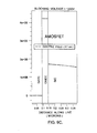
- Figures 8 and 9 show the advantageous electrical responses of a transistor formed according to this invention with a conductive channel on the A-face of silicon carbide.
- the figures compare traditional prior art DMOSFET ( Figures 8a , 9a) and UMOSFET ( Figures 8b , 9b) transistors with the AMOSFET ( Figures 8c , 9c) disclosed herein.
- Figure 8 is a schematic representation of electric field distribution for the three devices (DMOS, UMOS, AMOS) upon application of a 1200V blocking voltage on the gate contact of each.
- a DMOSFET of the prior art exhibits high field strength along the oxide insulating layer (15), thereby minimizing the reverse bias that the device can withstand before breaking down in that region.
- the prior art UMOSFET of Figure 8b shows a similar field crowding at the intersection of the gate contact and the semiconductor walls of the trench. Field crowding at the corner of the trench in Figure 8b prevents the device from achieving full voltage blocking characteristics.
- the AMOSFET formed according to this invention and shown in Figure 8c , includes the buffer layer (73) and the deep well (77) that protect the trench corners from the higher field in the trench.
- the trench corner of the AMOSFET of this invention is exposed to an electric field less than about 1.26e6 volts/cm, which is an improvement over the UMOSFET trench of Figure 8b which is exposed to a field strength of about 5e6 v/cm at the same blocking voltage.
- the AMOSFET of this invention is capable of withstanding higher reverse blocking voltages due to the improved design that includes the deep p+ well (77) and the n type buffer layer (73).
- Figure 9 illustrates the electric field in the oxide layer of each device from Figure 8 (DMOS, UMOS, and AMOS respectively).
- the field at the trench corner is 50 percent greater than the maximum electric filed in the AMOSFET oxide layer ( Figure 9c ).
- the AMOSFET ( Figure 9c ) also spreads the field throughout the silicon carbide more evenly as opposed to the drastic drop-off of the USMOSFET of Figure 9b .
- the field response for the UMOSFET exhibits the expected pattern of field crowding at the trench corner which hinders proper operation.
- the AMOSFET disclosed herein appropriately spreads the electric field evenly throughout the body of the device to enable a higher blocking voltage thereon.
- MOSFETs according to this invention optionally include a silicon carbide substrate formed by known means.
- a drift region (55) layer of 4H-SiC is epitaxially grown on a substrate, and then, in the enhanced embodiment of this invention, a buffer layer (73) of silicon carbide, typically doped to n-type, is formed on the drift region (55).
- the method includes forming at least one doped well region (77) of a first conductivity type, preferably P+.
- the well region (77) can be formed by any common technique but is preferably formed by implanting dopants into the semiconductor from the top of the device down to a depth that is greater than one micron.
- the method includes the steps of growing a first epitaxial layer (68) of a first conductivity type on the drift region (55) such that the first epitaxial layer (68) covers at least a portion of the doped well region (77).
- a second epitaxial layer (69) of a second conductivity type is formed on the first epitaxial layer (68).
- the body of the AMOSFET (50) at this point includes semiconductor layers, preferably of silicon carbide, for controlling electrical conduction from top to bottom.
- the next step in the process of this invention is that of etching the epitaxial layers, particularly the buffer layer (73) as well as the first and second epitaxial layers (68, 69) to form a trench within the semiconductor layers and thereby forming a pair of semiconductor mesas (65).
- the trench (56) preferably extends to a depth that is less than the depth of doped well region (77).
- a buried channel layer (72) is formed over at least a portion of the second epitaxial layer (69).
- the buried channel layer (72) extends into the trench (56), across the trench bottom, and continues to cover the opposite trench walls and at least a portion of the second mesa opposite the first.
- the trench wall is covered with a layer of gate insulation (64), such as silicon dioxide, on which the gate contact (61) is formed in the trench.
- the method of forming a transistor with a channel region along the A-face of a semiconductor body may include implanting a doped well region (77) of a first conductivity type in a semiconductor body (55) and then growing an epitaxial layer (68) of the first conductivity type on at least a portion of the well layer (77).
- the upper portion of the first epitaxial layer (68) may be converted to an opposite conductivity type by implanting techniques that are known in the art.
- This upper portion of second conductivity type is then the second epitaxial layer (69) for forming a pn junction within the transistor (50).
- Etching the epitaxial layers forms the desirable trench for forming a gate contact (61) that controls conduction.
- the method described herein can also be used to form other transistors that benefit from a highly conductive channel on the A-face of the semiconductor layers. Accordingly, this invention is not limited to MOSFETs, but is equally applicable to insulated gate bipolar transistors and metal-oxide-semiconductor controlled thyristors.
- the semiconductor material used for forming all of these devices is preferably silicon carbide, but the invention is not limited to such.
- transistors may include a p-type or n-type channel, depending upon configuration. Any layer or transistor region described herein may have an opposite doping type, as the descriptions used in this document are for example only.
Landscapes
- Junction Field-Effect Transistors (AREA)
- Insulated Gate Type Field-Effect Transistor (AREA)
Priority Applications (1)
| Application Number | Priority Date | Filing Date | Title |
|---|---|---|---|
| EP13161683.1A EP2615642A1 (de) | 2007-12-07 | 2008-12-05 | Transistor mit A-Seiten-Leitkanal und Grabenschutzbohrbereich |
Applications Claiming Priority (1)
| Application Number | Priority Date | Filing Date | Title |
|---|---|---|---|
| US11/952,447 US7989882B2 (en) | 2007-12-07 | 2007-12-07 | Transistor with A-face conductive channel and trench protecting well region |
Publications (2)
| Publication Number | Publication Date |
|---|---|
| EP2068363A2 true EP2068363A2 (de) | 2009-06-10 |
| EP2068363A3 EP2068363A3 (de) | 2010-06-02 |
Family
ID=40456434
Family Applications (2)
| Application Number | Title | Priority Date | Filing Date |
|---|---|---|---|
| EP08170802A Ceased EP2068363A3 (de) | 2007-12-07 | 2008-12-05 | MISFET mit Graben-Gate |
| EP13161683.1A Ceased EP2615642A1 (de) | 2007-12-07 | 2008-12-05 | Transistor mit A-Seiten-Leitkanal und Grabenschutzbohrbereich |
Family Applications After (1)
| Application Number | Title | Priority Date | Filing Date |
|---|---|---|---|
| EP13161683.1A Ceased EP2615642A1 (de) | 2007-12-07 | 2008-12-05 | Transistor mit A-Seiten-Leitkanal und Grabenschutzbohrbereich |
Country Status (3)
| Country | Link |
|---|---|
| US (3) | US7989882B2 (de) |
| EP (2) | EP2068363A3 (de) |
| JP (2) | JP5457017B2 (de) |
Cited By (9)
| Publication number | Priority date | Publication date | Assignee | Title |
|---|---|---|---|---|
| CN102194885A (zh) * | 2011-05-12 | 2011-09-21 | 西安电子科技大学 | N型隐埋沟道的碳化硅demosfet器件及制备方法 |
| CN102832248A (zh) * | 2012-09-10 | 2012-12-19 | 西安电子科技大学 | 基于半超结的碳化硅mosfet及制作方法 |
| EP2615642A1 (de) * | 2007-12-07 | 2013-07-17 | Cree, Inc. | Transistor mit A-Seiten-Leitkanal und Grabenschutzbohrbereich |
| WO2014105371A1 (en) * | 2012-12-28 | 2014-07-03 | Cree, Inc. | Transistor structures and methods for making the same |
| WO2014164294A1 (en) | 2013-03-13 | 2014-10-09 | Cree, Inc. | Field effect transistor devices with protective regions |
| US9530844B2 (en) | 2012-12-28 | 2016-12-27 | Cree, Inc. | Transistor structures having reduced electrical field at the gate oxide and methods for making same |
| US9570585B2 (en) | 2013-03-13 | 2017-02-14 | Cree, Inc. | Field effect transistor devices with buried well protection regions |
| US11417760B2 (en) | 2017-12-21 | 2022-08-16 | Wolfspeed, Inc. | Vertical semiconductor device with improved ruggedness |
| US11489069B2 (en) | 2017-12-21 | 2022-11-01 | Wolfspeed, Inc. | Vertical semiconductor device with improved ruggedness |
Families Citing this family (67)
| Publication number | Priority date | Publication date | Assignee | Title |
|---|---|---|---|---|
| US8432012B2 (en) | 2006-08-01 | 2013-04-30 | Cree, Inc. | Semiconductor devices including schottky diodes having overlapping doped regions and methods of fabricating same |
| US7728402B2 (en) | 2006-08-01 | 2010-06-01 | Cree, Inc. | Semiconductor devices including schottky diodes with controlled breakdown |
| US8421148B2 (en) * | 2007-09-14 | 2013-04-16 | Cree, Inc. | Grid-UMOSFET with electric field shielding of gate oxide |
| US7772621B2 (en) * | 2007-09-20 | 2010-08-10 | Infineon Technologies Austria Ag | Semiconductor device with structured current spread region and method |
| JP4798119B2 (ja) * | 2007-11-06 | 2011-10-19 | 株式会社デンソー | 炭化珪素半導体装置およびその製造方法 |
| US8232558B2 (en) | 2008-05-21 | 2012-07-31 | Cree, Inc. | Junction barrier Schottky diodes with current surge capability |
| US8193848B2 (en) | 2009-06-02 | 2012-06-05 | Cree, Inc. | Power switching devices having controllable surge current capabilities |
| US9117739B2 (en) * | 2010-03-08 | 2015-08-25 | Cree, Inc. | Semiconductor devices with heterojunction barrier regions and methods of fabricating same |
| US8415671B2 (en) | 2010-04-16 | 2013-04-09 | Cree, Inc. | Wide band-gap MOSFETs having a heterojunction under gate trenches thereof and related methods of forming such devices |
| US8525254B2 (en) * | 2010-08-12 | 2013-09-03 | Infineon Technologies Austria Ag | Silicone carbide trench semiconductor device |
| US9029945B2 (en) * | 2011-05-06 | 2015-05-12 | Cree, Inc. | Field effect transistor devices with low source resistance |
| US9142662B2 (en) * | 2011-05-06 | 2015-09-22 | Cree, Inc. | Field effect transistor devices with low source resistance |
| US8772788B2 (en) * | 2011-05-30 | 2014-07-08 | Panasonic Corporation | Semiconductor element and method of manufacturing thereof |
| JP2012253293A (ja) * | 2011-06-07 | 2012-12-20 | Sumitomo Electric Ind Ltd | 半導体装置 |
| CN103069571B (zh) * | 2011-06-27 | 2015-11-25 | 松下电器产业株式会社 | 碳化硅半导体元件及其制造方法 |
| KR101584023B1 (ko) * | 2011-08-26 | 2016-01-08 | 고쿠리츠다이가쿠호징 나라 센탄카가쿠기쥬츠 다이가쿠인 다이가쿠 | SiC반도체소자 및 그 제조방법 |
| US9373617B2 (en) | 2011-09-11 | 2016-06-21 | Cree, Inc. | High current, low switching loss SiC power module |
| US8664665B2 (en) | 2011-09-11 | 2014-03-04 | Cree, Inc. | Schottky diode employing recesses for elements of junction barrier array |
| WO2013036370A1 (en) | 2011-09-11 | 2013-03-14 | Cree, Inc. | High current density power module comprising transistors with improved layout |
| US8618582B2 (en) | 2011-09-11 | 2013-12-31 | Cree, Inc. | Edge termination structure employing recesses for edge termination elements |
| US8680587B2 (en) | 2011-09-11 | 2014-03-25 | Cree, Inc. | Schottky diode |
| US9640617B2 (en) | 2011-09-11 | 2017-05-02 | Cree, Inc. | High performance power module |
| JP2013145770A (ja) * | 2012-01-13 | 2013-07-25 | Sumitomo Electric Ind Ltd | 半導体装置およびその製造方法 |
| US8637922B1 (en) | 2012-07-19 | 2014-01-28 | Infineon Technologies Ag | Semiconductor device |
| US9006027B2 (en) | 2012-09-11 | 2015-04-14 | General Electric Company | Systems and methods for terminating junctions in wide bandgap semiconductor devices |
| WO2014073127A1 (ja) * | 2012-11-09 | 2014-05-15 | パナソニック株式会社 | 半導体装置及びその製造方法 |
| US9293558B2 (en) | 2012-11-26 | 2016-03-22 | Infineon Technologies Austria Ag | Semiconductor device |
| US9240476B2 (en) | 2013-03-13 | 2016-01-19 | Cree, Inc. | Field effect transistor devices with buried well regions and epitaxial layers |
| US9012984B2 (en) | 2013-03-13 | 2015-04-21 | Cree, Inc. | Field effect transistor devices with regrown p-layers |
| US9024328B2 (en) | 2013-07-02 | 2015-05-05 | General Electric Company | Metal-oxide-semiconductor (MOS) devices with increased channel periphery and methods of manufacture |
| US9748341B2 (en) | 2013-07-02 | 2017-08-29 | General Electric Company | Metal-oxide-semiconductor (MOS) devices with increased channel periphery |
| WO2015010121A1 (en) * | 2013-07-19 | 2015-01-22 | Ramgoss, Inc. | Self-aligned gate buried channel field effect transistor |
| US9768259B2 (en) * | 2013-07-26 | 2017-09-19 | Cree, Inc. | Controlled ion implantation into silicon carbide using channeling and devices fabricated using controlled ion implantation into silicon carbide using channeling |
| US9331197B2 (en) | 2013-08-08 | 2016-05-03 | Cree, Inc. | Vertical power transistor device |
| US10600903B2 (en) | 2013-09-20 | 2020-03-24 | Cree, Inc. | Semiconductor device including a power transistor device and bypass diode |
| US20150084063A1 (en) * | 2013-09-20 | 2015-03-26 | Cree, Inc. | Semiconductor device with a current spreading layer |
| US10868169B2 (en) * | 2013-09-20 | 2020-12-15 | Cree, Inc. | Monolithically integrated vertical power transistor and bypass diode |
| US10211304B2 (en) * | 2013-12-04 | 2019-02-19 | General Electric Company | Semiconductor device having gate trench in JFET region |
| JP6179409B2 (ja) | 2014-01-24 | 2017-08-16 | 株式会社デンソー | 炭化珪素半導体装置の製造方法 |
| CN104319292A (zh) * | 2014-11-06 | 2015-01-28 | 株洲南车时代电气股份有限公司 | 一种新型碳化硅mosfet及其制造方法 |
| DE102014117780B4 (de) | 2014-12-03 | 2018-06-21 | Infineon Technologies Ag | Halbleiterbauelement mit einer Grabenelektrode und Verfahren zur Herstellung |
| US9577073B2 (en) | 2014-12-11 | 2017-02-21 | Infineon Technologies Ag | Method of forming a silicon-carbide device with a shielded gate |
| DE102014119465B3 (de) | 2014-12-22 | 2016-05-25 | Infineon Technologies Ag | Halbleitervorrichtung mit streifenförmigen trenchgatestrukturen, transistormesas und diodenmesas |
| US9466709B2 (en) | 2014-12-26 | 2016-10-11 | Fairchild Semiconductor Corporation | Silicon-carbide trench gate MOSFETs |
| US9893176B2 (en) | 2014-12-26 | 2018-02-13 | Fairchild Semiconductor Corporation | Silicon-carbide trench gate MOSFETs |
| JP6485299B2 (ja) * | 2015-06-05 | 2019-03-20 | 豊田合成株式会社 | 半導体装置およびその製造方法ならびに電力変換装置 |
| JP6400548B2 (ja) * | 2015-09-14 | 2018-10-03 | 株式会社東芝 | 半導体装置 |
| CN105185833B (zh) * | 2015-09-25 | 2020-01-03 | 国网智能电网研究院 | 一种隐埋沟道碳化硅沟槽栅MOSFETs器件及其制备方法 |
| US10340374B2 (en) * | 2015-09-25 | 2019-07-02 | Intel Corporation | High mobility field effect transistors with a retrograded semiconductor source/drain |
| DE102016226237B4 (de) | 2016-02-01 | 2024-07-18 | Fuji Electric Co., Ltd. | Siliziumcarbid-halbleitervorrichtung |
| JP6115678B1 (ja) | 2016-02-01 | 2017-04-19 | 富士電機株式会社 | 炭化珪素半導体装置および炭化珪素半導体装置の製造方法 |
| US10861931B2 (en) | 2016-12-08 | 2020-12-08 | Cree, Inc. | Power semiconductor devices having gate trenches and buried edge terminations and related methods |
| US9887287B1 (en) | 2016-12-08 | 2018-02-06 | Cree, Inc. | Power semiconductor devices having gate trenches with implanted sidewalls and related methods |
| DE102018103973B4 (de) | 2018-02-22 | 2020-12-03 | Infineon Technologies Ag | Siliziumcarbid-halbleiterbauelement |
| DE102019111308A1 (de) | 2018-05-07 | 2019-11-07 | Infineon Technologies Ag | Siliziumcarbid halbleiterbauelement |
| DE102018124740B4 (de) | 2018-10-08 | 2025-08-28 | Infineon Technologies Ag | Verfahren zur herstellung eines halbleiterbauelements |
| US10586845B1 (en) | 2018-11-16 | 2020-03-10 | Infineon Technologies Ag | SiC trench transistor device and methods of manufacturing thereof |
| US10903322B2 (en) | 2018-11-16 | 2021-01-26 | Infineon Technologies Ag | SiC power semiconductor device with integrated body diode |
| US10985248B2 (en) | 2018-11-16 | 2021-04-20 | Infineon Technologies Ag | SiC power semiconductor device with integrated Schottky junction |
| US11139394B2 (en) * | 2019-08-30 | 2021-10-05 | Semiconductor Components Industries, Llc | Silicon carbide field-effect transistors |
| DE102020004758A1 (de) * | 2019-08-30 | 2021-03-04 | Semiconductor Components Industries, Llc | Siliciumcarbid-feldeffekttransistoren |
| US12094926B2 (en) | 2020-08-14 | 2024-09-17 | Wolfspeed, Inc. | Sidewall dopant shielding methods and approaches for trenched semiconductor device structures |
| US11355630B2 (en) | 2020-09-11 | 2022-06-07 | Wolfspeed, Inc. | Trench bottom shielding methods and approaches for trenched semiconductor device structures |
| CN115588668A (zh) * | 2021-07-06 | 2023-01-10 | 现代摩比斯株式会社 | 功率半导体器件及制造其的方法 |
| WO2024006912A1 (en) * | 2022-07-01 | 2024-01-04 | The Research Foundation For The State University Of New York | Metal oxide semiconductor field effect transistors (mosfet) with bottom p-wells and deep p-wells |
| CN116469923B (zh) * | 2023-04-25 | 2023-10-20 | 南京第三代半导体技术创新中心有限公司 | 高可靠性沟槽型碳化硅mosfet器件及其制造方法 |
| CN116884997B (zh) * | 2023-09-07 | 2023-12-22 | 珠海格力电子元器件有限公司 | 绝缘栅双极型晶体管及其制备方法 |
Citations (2)
| Publication number | Priority date | Publication date | Assignee | Title |
|---|---|---|---|---|
| US5976936A (en) | 1995-09-06 | 1999-11-02 | Denso Corporation | Silicon carbide semiconductor device |
| JP2001267570A (ja) * | 2000-03-15 | 2001-09-28 | Mitsubishi Electric Corp | 半導体装置及び半導体装置製造方法 |
Family Cites Families (37)
| Publication number | Priority date | Publication date | Assignee | Title |
|---|---|---|---|---|
| US5440160A (en) * | 1992-01-28 | 1995-08-08 | Thunderbird Technologies, Inc. | High saturation current, low leakage current fermi threshold field effect transistor |
| IT1272567B (it) * | 1992-09-15 | 1997-06-23 | Int Rectifier Corp | Dispositivo transistore di potenza, dotato di una regione ultraprofonda a concentrazione maggiorata |
| US5561302A (en) * | 1994-09-26 | 1996-10-01 | Motorola, Inc. | Enhanced mobility MOSFET device and method |
| US6075259A (en) * | 1994-11-14 | 2000-06-13 | North Carolina State University | Power semiconductor devices that utilize buried insulating regions to achieve higher than parallel-plane breakdown voltages |
| US5688725A (en) * | 1994-12-30 | 1997-11-18 | Siliconix Incorporated | Method of making a trench mosfet with heavily doped delta layer to provide low on-resistance |
| US6573534B1 (en) * | 1995-09-06 | 2003-06-03 | Denso Corporation | Silicon carbide semiconductor device |
| US5742076A (en) * | 1996-06-05 | 1998-04-21 | North Carolina State University | Silicon carbide switching devices having near ideal breakdown voltage capability and ultralow on-state resistance |
| JP3719323B2 (ja) | 1997-03-05 | 2005-11-24 | 株式会社デンソー | 炭化珪素半導体装置 |
| US6057558A (en) * | 1997-03-05 | 2000-05-02 | Denson Corporation | Silicon carbide semiconductor device and manufacturing method thereof |
| US6465842B2 (en) * | 1998-06-25 | 2002-10-15 | Kabushiki Kaisha Toshiba | MIS semiconductor device and method of fabricating the same |
| US6724053B1 (en) | 2000-02-23 | 2004-04-20 | International Business Machines Corporation | PMOSFET device with localized nitrogen sidewall implantation |
| US6784486B2 (en) * | 2000-06-23 | 2004-08-31 | Silicon Semiconductor Corporation | Vertical power devices having retrograded-doped transition regions therein |
| US6781194B2 (en) * | 2001-04-11 | 2004-08-24 | Silicon Semiconductor Corporation | Vertical power devices having retrograded-doped transition regions and insulated trench-based electrodes therein |
| US6921939B2 (en) | 2000-07-20 | 2005-07-26 | Fairchild Semiconductor Corporation | Power MOSFET and method for forming same using a self-aligned body implant |
| US6586833B2 (en) * | 2000-11-16 | 2003-07-01 | Silicon Semiconductor Corporation | Packaged power devices having vertical power mosfets therein that are flip-chip mounted to slotted gate electrode strip lines |
| JP4830213B2 (ja) * | 2001-05-08 | 2011-12-07 | 株式会社デンソー | 炭化珪素半導体装置及びその製造方法 |
| JP4839548B2 (ja) * | 2001-08-29 | 2011-12-21 | 株式会社デンソー | 炭化珪素半導体装置及びその製造方法 |
| JP3973395B2 (ja) * | 2001-10-16 | 2007-09-12 | 株式会社豊田中央研究所 | 半導体装置とその製造方法 |
| JP3539417B2 (ja) * | 2001-11-14 | 2004-07-07 | 日産自動車株式会社 | 炭化珪素半導体装置及びその製造方法 |
| US6919599B2 (en) * | 2002-06-28 | 2005-07-19 | International Rectifier Corporation | Short channel trench MOSFET with reduced gate charge |
| EP1630872B1 (de) * | 2003-06-05 | 2016-12-28 | Mitsubishi Denki Kabushiki Kaisha | Halbleiterbauelement und verfahren zu seiner herstellung |
| US7709403B2 (en) * | 2003-10-09 | 2010-05-04 | Panasonic Corporation | Silicon carbide-oxide layered structure, production method thereof, and semiconductor device |
| TWI256676B (en) | 2004-03-26 | 2006-06-11 | Siliconix Inc | Termination for trench MIS device having implanted drain-drift region |
| SE527205C2 (sv) * | 2004-04-14 | 2006-01-17 | Denso Corp | Förfarande för tillverkning av halvledaranordning med kanal i halvledarsubstrat av kiselkarbid |
| JP2006100365A (ja) | 2004-09-28 | 2006-04-13 | Nissan Motor Co Ltd | 半導体装置 |
| JP4899405B2 (ja) | 2004-11-08 | 2012-03-21 | 株式会社デンソー | 炭化珪素半導体装置およびその製造方法 |
| JP2006228906A (ja) * | 2005-02-16 | 2006-08-31 | Sanyo Electric Co Ltd | 半導体装置およびその製造方法 |
| JP2006344759A (ja) * | 2005-06-08 | 2006-12-21 | Sharp Corp | トレンチ型mosfet及びその製造方法 |
| JP4957005B2 (ja) | 2006-01-31 | 2012-06-20 | 富士電機株式会社 | 炭化珪素半導体素子の製造方法 |
| JP5194380B2 (ja) | 2006-04-28 | 2013-05-08 | 日産自動車株式会社 | 半導体装置 |
| US7883949B2 (en) * | 2006-06-29 | 2011-02-08 | Cree, Inc | Methods of forming silicon carbide switching devices including P-type channels |
| US8710510B2 (en) * | 2006-08-17 | 2014-04-29 | Cree, Inc. | High power insulated gate bipolar transistors |
| US7476932B2 (en) * | 2006-09-29 | 2009-01-13 | The Boeing Company | U-shape metal-oxide-semiconductor (UMOS) gate structure for high power MOS-based semiconductor devices |
| US7589377B2 (en) * | 2006-10-06 | 2009-09-15 | The Boeing Company | Gate structure with low resistance for high power semiconductor devices |
| US7598567B2 (en) * | 2006-11-03 | 2009-10-06 | Cree, Inc. | Power switching semiconductor devices including rectifying junction-shunts |
| JP4798119B2 (ja) * | 2007-11-06 | 2011-10-19 | 株式会社デンソー | 炭化珪素半導体装置およびその製造方法 |
| US7989882B2 (en) * | 2007-12-07 | 2011-08-02 | Cree, Inc. | Transistor with A-face conductive channel and trench protecting well region |
-
2007
- 2007-12-07 US US11/952,447 patent/US7989882B2/en active Active
-
2008
- 2008-12-04 JP JP2008310327A patent/JP5457017B2/ja active Active
- 2008-12-05 EP EP08170802A patent/EP2068363A3/de not_active Ceased
- 2008-12-05 EP EP13161683.1A patent/EP2615642A1/de not_active Ceased
-
2011
- 2011-06-24 US US13/167,806 patent/US8211770B2/en active Active
-
2012
- 2012-05-29 US US13/482,311 patent/US9064710B2/en active Active
-
2013
- 2013-01-17 JP JP2013006010A patent/JP2013065907A/ja active Pending
Patent Citations (2)
| Publication number | Priority date | Publication date | Assignee | Title |
|---|---|---|---|---|
| US5976936A (en) | 1995-09-06 | 1999-11-02 | Denso Corporation | Silicon carbide semiconductor device |
| JP2001267570A (ja) * | 2000-03-15 | 2001-09-28 | Mitsubishi Electric Corp | 半導体装置及び半導体装置製造方法 |
Non-Patent Citations (4)
| Title |
|---|
| TAN J ET AL: "High-Voltage Accumulation-Layer UMOSFET's in 4H-SiC", 19981201, vol. 19, no. 12, 1 December 1998 (1998-12-01), XP011018515 * |
| YANO ET AL.: "High Channel Mobility in Inversion Layers of 4H-SiC MOSFETs by Utilizing (1120) Face", IEEE ELECTRON DEVICE LETTERS, vol. 20, no. 12, December 1999 (1999-12-01), pages 611 - 613, XP002698013, DOI: doi:10.1109/55.806101 |
| YANO H ET AL: "HIGH CHANNEL MOBILITY IN INVERSION LAYER OF SIC MOSFETS FOR POWER SWITCHING TRANSISTORS", EXTENDED ABSTRACTS OF THE INTERNATIONAL CONFERENCE ON SOLIDSTATE DEVICES AND MATERIALS, JAPAN SOCIETY OF APPLIED PHYSICS. TOKYO, JA, 1 January 1999 (1999-01-01), pages 372/373, XP000935127 * |
| ZETTERLING; CARL-MIKAEL: "Process Technology for Silicon Carbide Devices", 2002, INSTITUTE OF ELECTRICAL ENGINEERS, pages: 3 |
Cited By (17)
| Publication number | Priority date | Publication date | Assignee | Title |
|---|---|---|---|---|
| EP2615642A1 (de) * | 2007-12-07 | 2013-07-17 | Cree, Inc. | Transistor mit A-Seiten-Leitkanal und Grabenschutzbohrbereich |
| US9064710B2 (en) | 2007-12-07 | 2015-06-23 | Cree, Inc. | Transistor with A-face conductive channel and trench protecting well region |
| CN102194885A (zh) * | 2011-05-12 | 2011-09-21 | 西安电子科技大学 | N型隐埋沟道的碳化硅demosfet器件及制备方法 |
| CN102832248A (zh) * | 2012-09-10 | 2012-12-19 | 西安电子科技大学 | 基于半超结的碳化硅mosfet及制作方法 |
| US10115815B2 (en) | 2012-12-28 | 2018-10-30 | Cree, Inc. | Transistor structures having a deep recessed P+ junction and methods for making same |
| WO2014105371A1 (en) * | 2012-12-28 | 2014-07-03 | Cree, Inc. | Transistor structures and methods for making the same |
| US10886396B2 (en) | 2012-12-28 | 2021-01-05 | Cree, Inc. | Transistor structures having a deep recessed P+ junction and methods for making same |
| US9530844B2 (en) | 2012-12-28 | 2016-12-27 | Cree, Inc. | Transistor structures having reduced electrical field at the gate oxide and methods for making same |
| US10840367B2 (en) | 2012-12-28 | 2020-11-17 | Cree, Inc. | Transistor structures having reduced electrical field at the gate oxide and methods for making same |
| WO2014164294A1 (en) | 2013-03-13 | 2014-10-09 | Cree, Inc. | Field effect transistor devices with protective regions |
| US10134834B2 (en) | 2013-03-13 | 2018-11-20 | Cree, Inc. | Field effect transistor devices with buried well protection regions |
| US10784338B2 (en) | 2013-03-13 | 2020-09-22 | Cree, Inc. | Field effect transistor devices with buried well protection regions |
| US9570585B2 (en) | 2013-03-13 | 2017-02-14 | Cree, Inc. | Field effect transistor devices with buried well protection regions |
| EP2973723A4 (de) * | 2013-03-13 | 2016-11-09 | Cree Inc | Feldeffekttransistoren mit schutzbereichen |
| US11417760B2 (en) | 2017-12-21 | 2022-08-16 | Wolfspeed, Inc. | Vertical semiconductor device with improved ruggedness |
| US11489069B2 (en) | 2017-12-21 | 2022-11-01 | Wolfspeed, Inc. | Vertical semiconductor device with improved ruggedness |
| US12087854B2 (en) | 2017-12-21 | 2024-09-10 | Wolfspeed, Inc. | Vertical semiconductor device with improved ruggedness |
Also Published As
| Publication number | Publication date |
|---|---|
| JP5457017B2 (ja) | 2014-04-02 |
| EP2068363A3 (de) | 2010-06-02 |
| JP2013065907A (ja) | 2013-04-11 |
| US20090146154A1 (en) | 2009-06-11 |
| US20110250737A1 (en) | 2011-10-13 |
| US8211770B2 (en) | 2012-07-03 |
| EP2615642A1 (de) | 2013-07-17 |
| US9064710B2 (en) | 2015-06-23 |
| JP2009141363A (ja) | 2009-06-25 |
| US20120235164A1 (en) | 2012-09-20 |
| US7989882B2 (en) | 2011-08-02 |
Similar Documents
| Publication | Publication Date | Title |
|---|---|---|
| US8211770B2 (en) | Transistor with A-face conductive channel and trench protecting well region | |
| US10840367B2 (en) | Transistor structures having reduced electrical field at the gate oxide and methods for making same | |
| US9093493B2 (en) | Wide bandgap insulated gate semiconductor device | |
| CN107112276B (zh) | 具有带锥形氧化物厚度的多晶硅填充渠沟的功率组件 | |
| EP1095409B1 (de) | Halbleiterbaulelemente aus silizium-karbid mit horizontalem kanal und gepuffertem gate | |
| JP3385938B2 (ja) | 炭化珪素半導体装置及びその製造方法 | |
| US9419092B2 (en) | Termination for SiC trench devices | |
| US10157979B2 (en) | High voltage semiconductor device with reduced peak electric field in active and termination areas of the device | |
| US7719080B2 (en) | Semiconductor device with a conduction enhancement layer | |
| US20070007537A1 (en) | Semiconductor device | |
| US20230094032A1 (en) | Method of producing a silicon carbide device with a trench gate | |
| US20190393299A1 (en) | Silicon Carbide Semiconductor Device | |
| US20240339494A1 (en) | Vertical mosfet with high short circuit withstand time capability | |
| US20260101553A1 (en) | Semiconductor devices with length-graded channel | |
| JP7796550B2 (ja) | 半導体装置 | |
| KR20250041730A (ko) | 높은 항복 전압을 갖는 트렌치형 전력반도체소자의 제조 방법 및 이를 이용하여 제조된 높은 항복 전압을 갖는 트렌치형 전력반도체소자 | |
| CN118610270A (zh) | 一种沟槽型碳化硅器件结构及其制造方法 |
Legal Events
| Date | Code | Title | Description |
|---|---|---|---|
| PUAI | Public reference made under article 153(3) epc to a published international application that has entered the european phase |
Free format text: ORIGINAL CODE: 0009012 |
|
| 17P | Request for examination filed |
Effective date: 20081205 |
|
| AK | Designated contracting states |
Kind code of ref document: A2 Designated state(s): AT BE BG CH CY CZ DE DK EE ES FI FR GB GR HR HU IE IS IT LI LT LU LV MC MT NL NO PL PT RO SE SI SK TR |
|
| AX | Request for extension of the european patent |
Extension state: AL BA MK RS |
|
| PUAL | Search report despatched |
Free format text: ORIGINAL CODE: 0009013 |
|
| AK | Designated contracting states |
Kind code of ref document: A3 Designated state(s): AT BE BG CH CY CZ DE DK EE ES FI FR GB GR HR HU IE IS IT LI LT LU LV MC MT NL NO PL PT RO SE SI SK TR |
|
| AX | Request for extension of the european patent |
Extension state: AL BA MK RS |
|
| AKX | Designation fees paid |
Designated state(s): AT BE BG CH CY CZ DE DK EE ES FI FR GB GR HR HU IE IS IT LI LT LU LV MC MT NL NO PL PT RO SE SI SK TR |
|
| 17Q | First examination report despatched |
Effective date: 20110329 |
|
| APBK | Appeal reference recorded |
Free format text: ORIGINAL CODE: EPIDOSNREFNE |
|
| APBN | Date of receipt of notice of appeal recorded |
Free format text: ORIGINAL CODE: EPIDOSNNOA2E |
|
| APBR | Date of receipt of statement of grounds of appeal recorded |
Free format text: ORIGINAL CODE: EPIDOSNNOA3E |
|
| APAF | Appeal reference modified |
Free format text: ORIGINAL CODE: EPIDOSCREFNE |
|
| APBT | Appeal procedure closed |
Free format text: ORIGINAL CODE: EPIDOSNNOA9E |
|
| STAA | Information on the status of an ep patent application or granted ep patent |
Free format text: STATUS: THE APPLICATION HAS BEEN REFUSED |
|
| 18R | Application refused |
Effective date: 20190709 |