EP2068368A2 - Procédé de fabrication de matériau de chalcogénure de type N et de type P, transistor à couche mince de matériau de chalcogénure dopé et son procédé de fabrication - Google Patents
Procédé de fabrication de matériau de chalcogénure de type N et de type P, transistor à couche mince de matériau de chalcogénure dopé et son procédé de fabrication Download PDFInfo
- Publication number
- EP2068368A2 EP2068368A2 EP08170842A EP08170842A EP2068368A2 EP 2068368 A2 EP2068368 A2 EP 2068368A2 EP 08170842 A EP08170842 A EP 08170842A EP 08170842 A EP08170842 A EP 08170842A EP 2068368 A2 EP2068368 A2 EP 2068368A2
- Authority
- EP
- European Patent Office
- Prior art keywords
- chalcogenide
- type
- layer
- thin film
- film transistor
- Prior art date
- Legal status (The legal status is an assumption and is not a legal conclusion. Google has not performed a legal analysis and makes no representation as to the accuracy of the status listed.)
- Granted
Links
Images


Classifications
-
- H—ELECTRICITY
- H10—SEMICONDUCTOR DEVICES; ELECTRIC SOLID-STATE DEVICES NOT OTHERWISE PROVIDED FOR
- H10D—INORGANIC ELECTRIC SEMICONDUCTOR DEVICES
- H10D30/00—Field-effect transistors [FET]
- H10D30/60—Insulated-gate field-effect transistors [IGFET]
- H10D30/67—Thin-film transistors [TFT]
- H10D30/674—Thin-film transistors [TFT] characterised by the active materials
- H10D30/675—Group III-V materials, Group II-VI materials, Group IV-VI materials, selenium or tellurium
-
- H—ELECTRICITY
- H10—SEMICONDUCTOR DEVICES; ELECTRIC SOLID-STATE DEVICES NOT OTHERWISE PROVIDED FOR
- H10D—INORGANIC ELECTRIC SEMICONDUCTOR DEVICES
- H10D62/00—Semiconductor bodies, or regions thereof, of devices having potential barriers
- H10D62/80—Semiconductor bodies, or regions thereof, of devices having potential barriers characterised by the materials
- H10D62/881—Semiconductor bodies, or regions thereof, of devices having potential barriers characterised by the materials being a two-dimensional material
Definitions
- the present invention relates to a method for manufacturing N-type and P-type chalcogenide materials, a doped homojunction chalcogenide thin film transistor and a method of fabricating the same. More particularly, the present invention relates to a method for manufacturing an N-type chalcogenide material and a P-type chalcogenide material, and a method of fabricating a doped homojunction chalcogenide thin film transistor using the N-type chalcogenide material and P-type chalcogenide material.
- CMOS complementary metal-oxide-semiconductor
- a low-cost low-temperature processed photo conductive thin film transistor (Photo-TFT) having relatively high-efficiency photo conductivity can be fabricated using unique characteristics of elements such as GeTe-Sb 2 Te 3 (Ge 2 Sb 2 Te 5 :GST) including chalcogenide-based elements on a periodic table.
- an undoped homojunction chalcogenide thin film transistor can be fabricated using a diode function expected from a principle to form a potential barrier generated from differences between charge concentration by a lone pair electron state of amorphous germanium antimony telluride (Ge 2 Sb 2 Te 5 ) including the chalcogenide-based elements and charge concentration by a vacancy state of the same material Ge 2 Sb 2 Te 5 .
- N-type and P-type chalcogenide materials by adding oxygen O 2 including chalcogenide based elements based on the periodic table and a method of fabricating a thin type transistor using the manufactured N-type and P-type chalcogenide material, as described in the present invention, have not been publicly known.
- Prior art 1 which has features that if predetermined light is applied to Ge 2 Sb 2 Te 5 , its phase is changed from amorphous to crystalline or from crystalline to amorphous, determines on whether or not Ge 2 Sb 2 Te 5 can be applied to optical information storage using an optically configured optical pick-up, if the result of the phase change is used.
- Prior art 2 which has been proposed by Ovsinsky, the first proposer of a Ge 2 Sb 2 Te 5 based phase change material, relates to a non-volatile memory PRAM using a phase change, that is, a method of applying a phase change phenomenon to an electric memory.
- This technique relates to a method of applying a switching phenomenon shown by mutually moving crystalline phases to the electric memory.
- Prior art 3 relates to a thesis of an electric memory transistor that is fabricated using Ge 2 Sb 2 Te 5 and the results of measured characteristics of the electric memory transistor is published.
- the prior art 3 basically corresponds to a method using a phase change mechanism obtained in the prior art 1 and the prior art 2, and relates to a method to apply the switching phenomenon which shows the states of mutually moving phases to the crystalline phase or the amorphous phase to a memory and a TFT.
- a chalcogenide material has been known as a material having typical P-type conductivity due to unique characteristics of its atomic structure.
- the main factor to show the P-type conductivity has been known to be generated by a vacancy state within a band gap and owing to the unique characteristics of such an atomic structure, an N-type chalcogenide material has not been developed up to now.
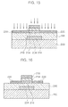
- FIG. 1 is a concept view of a structure of a photo thin film transistor fabricated using a general CMOS process. A structure of a photo thin film transistor actually fabricated through a CMOS process is more complicated.
- an amorphous silicon film 110 is formed on a silicon substrate 100 doped with impurity.
- Source and drain ohmic contact parts 120 for improving ohmic contacts are formed at both sides of the amorphous silicon film 110.
- the ohmic contact parts 120 are formed by ion-implanting the impurity into portions of the amorphous silicon film 110.
- a source electrode 140 and a drain electrode 150 are formed on the source and drain ohmic contact parts 120, respectively.
- a gate insulating film 130 is formed on the amorphous silicon film 110, the ohmic contact parts 120, and the source and drain electrodes 150.
- the gate insulating film 130 is formed using an oxide film.
- a gate electrode is formed on the gate insulating film 130 using a metal film 160.
- the thin film transistor fabricated using the CMOS process of FIG. 1 uses a high-cost silicon substrate and requires the ion-implantation process for forming the ohmic contact parts.
- the thin film transistor must also need the hydrogenated and doped ohmic contact parts.
- TFTs currently used in a TFT-LCD display and/or a mobile phone or the like have the structure of FIG. 1 .
- a channel layer of the TFT in order to utilize a layer having reference numeral 110 of FIG. 1 as a channel layer, a channel layer of the TFT should be first an N-type material or a P-type material, and in contrast, the ohmic contact parts having reference numeral 120 should be the P-type material or the N-type material.
- Such a structure has been known as the typical structure of the best transistor.
- the present invention is contrived to solve the above problems.
- a method for manufacturing an N-type chalcogenide material according to the present invention comprises:
- the chalcogenide material is Ge 2 Sb 2 Te 5 .
- a method for manufacturing a P-type chalcogenide material according to the present invention comprises: depositing Te alloy on an N-type chalcogenide material; and diffusing the N-type chalcogenide material on which the Te alloy is deposited.
- the Te alloy is one selected from the group consisting of GeTe, SbTe and Te.
- the diffusing the N-type chalcogenide material on which the Te alloy is deposited comprises applying heat energy to the N-type chalcogenide material on which the Te alloy is deposited.
- a method of fabricating a chalcogenide thin film transistor comprises: forming an N-type chalcogenide layer constituting a channel layer on a substrate; forming and patterning a diffusion prevention layer on the upper part of the N-type chalcogenide layer; and forming a P-type chalcogenide layer constituting source and drain regions by depositing and diffusing Te alloy on the N-type chalcogenide layer.
- the substrate is any one of a glass substrate, a plastic substrate, a polyimide substrate and a vinyl substrate.
- the chalcogenide layer is forming a Ge 2 Sb 2 Te 5 layer.
- the method of fabricating the chalcogenide thin film transistor further comprises forming a gate electrode by interposing a gate oxide at the bottom of the N-type chalcogenide layer constituting the channel layer.
- the gate oxide is a polymer PMMA film that is organic material.
- the gate oxide is a silicon oxide film formed using a PECVD method.
- a thin film transistor comprises: a chalcogenide layer forming a channel layer and constituting a first type conductivity; a chalcogenide layer formed on both sides of the chalcogenide layer having the first type conductivity to constitute source and drain regions and having a second type conductivity; and source and drain electrodes connected to the chalcogenide layer constituting the source and drain regions and having the second conductivity.
- the chalcogenide layer constituting the channel layer and the source and drain regions is a Ge 2 Sb 2 Te 5 layer.
- the thin film transistor further comprises a gate electrode formed by interposing a gate oxide at the bottom of the chalcogenide layer having the first conductivity.
- the gate oxide is a polymer PMMA film that is an organic material.
- the gate oxide is a silicon oxide film formed by a PECVD method.
- a diffusion prevention layer is formed on the upper part of the chalcogenide layer having the first conductivity.
- the channel layer is N-type, and the source and drain regions are P-type.
- the channel layer is P-type, and the source and drain regions are N-type.
- the present invention uses a chalcogenide layer, which is actively used or can be used as a material for a next generation non-volatile memory device in the field of information storage.
- a chalcogenide layer As an example of the chalcogenide layer, a GeTe-Sb 2 Te 3 layer (Ge 2 Sb 2 Te 3 , hereinafter, referred to as 'a GST layer') is used.
- the GST layer is exemplified as the chalcogenide layer, the present invention is not limited thereto.
- the chalcogenide layer used in the present invention has high efficiency photo conductivity, such that it may be used as a photo conductive layer of a photo thin film transistor (Photo TFT). Furthermore, in the chalcogenide layer of the present invention, a phase change can be made from amorphous to crystalline or crystalline to amorphous by means of laser or heat energy.
- the thin film transistor of the present invention can also be formed on a glass substrate using a Low-cost and low-temperature process.
- the chalcogenide layer can be formed of only P-type semiconductor.
- a plurality of P-type charges depend on the state of a lone pair electrons in an amorphous phase.
- the Fermi level (Ef) of the amorphous chalcogenide layer has a P-type semiconductor shape close to an intrinsic level (Ei), and a difference in charge concentration (a difference in carrier concentration) between the intrinsic level (Ei) and the Fermi level (Ef) has a small value, i.e., ⁇ p2.
- a band gap (Egp2) between a valence band (Ev) and a conduction band (Ec) of the amorphous chalcogenide layer is 0.7eV.
- the lone pair electron state in the amorphous state is disappeared and as a result, the characteristics of the P-type semiconductor are occur by the plurality of charges generated by a vacancy state generated from an atomic structure having the periodical crystalline phase.
- the N-type chalcogenide material has not been developed using a doping method.
- the present invention proposes a method capable of developing a chalcogenide material (hereinafter, referred to as 'N-type chalcogenide material) which shows the N-type semiconductor characteristics by injecting oxygen into the chalcogenide material having such a defect, that is, showing the P-type semiconductor characteristics.
- 'N-type chalcogenide material a chalcogenide material which shows the N-type semiconductor characteristics by injecting oxygen into the chalcogenide material having such a defect, that is, showing the P-type semiconductor characteristics.
- a chalcogenide material for example, GST
- a device used in depositing the chalcogenide material is a sputter device (for example, an RF magnetron sputter), which is typically used in depositing the chalcogenide material.
- a heat deposition apparatus other than the sputter may also be used.
- Ar argon
- FIG. 2 is a graph showing transmittance characteristics of the chalcogenide material generally deposited according to the above-described method.
- a band gap is 0.7eV (a wavelength band of about 1700 nm) as shown in FIG. 2 . If the amorphous chalcogenide deposited as above is crystallized, the band gap becomes about 0.5eV, such that a light transmittance curve becomes a curve having a long wavelength.
- oxygen is added to a deposition chamber when the amorphous chalcogenide is manufactured, as shown in FIG. 3 .
- the chalcogenide material is disposed as the target layer.
- oxygen gas in addition to the argon gas is simultaneously injected into the deposition chamber. Then, some of the injected oxygen gas is injected into a chalcogenide thin film to be deposited, and the N-type chalcogenide material is formed by the injected oxygen.
- high frequency energy is supplied to a sputter gun (not shown) so that a mixture of the argon gas and oxygen gas is ionized, thereby generating plasma.
- Ions of the ionized argon and oxygen gas collide with a target to sputter the target material in the generated plasma, such that chalcogenide material is deposited on the substrate.
- the oxygen gas as well as the argon gas are simultaneously injected and deposited in order to deposit the N-type chalcognide material.
- the N-type chalcognide material can be deposited according to a change in proportion of the amount of argon gas and oxygen gas injected at this time.
- the thickness of the deposited N-type chalcogenide material is controlled by a deposition time.
- the oxy-doped and deposited chalcogenide material is amorphous through an X-ray diffraction (SRD) measurement.
- FIG. 4 shows results of measuring light transmittance curves of chalcogenide material varying when the oxygen gas and the argon gas are injected to the sputter, in the proportions of the amount of oxygen gas/argon gas used in the present invention, such as 0.1, 0.25, 0.35 and 0.5, respectively. It can be appreciated that as the amount of injected oxygen increases, the band gap moves to have a short wavelength. It can be appreciated that when the proportions of the amount of injected oxygen gas/argon gas are 0.1, 0.25, 0.35 and 0.5, respectively, the band gap energy moves to have about 1300 nm, 1200 nm, 1100 nm, and 1000 nm band of wavelength, respectively.
- the reason why the bending is generated from the long wavelength (after 1400 nm) of the light transmittance curve in FIG. 4 is a typical phenomenon generated due to light interference, and thus does not have an important meaning in expecting the band gap.
- Table 1 shows a result of measuring the hall effects of the chalcogenide material manufactured using different injection proportions of the amount of oxygen gas/argon gas. Through the hall effect, the type , the concentration, the mobility and the like of a plurality of carriers can be appreciated. [Table 1] Injection proportion of the amount of oxygen gas/argon gas Carrier concentration (/cm ⁇ 2) 0.1 -1.2e15 0.25 -6.99e14 0.35 -5.5e14
- the N-type chalcogenide material is formed regardless of the amount of injected oxygen, when the injection proportion of the amount of oxygen gas/argon gas is from 0.1 to 0.35.
- the N-type chalcogenide material is expected to be formed even when the injection proportion of the amount of oxygen gas/argon gas is after 0.35, if there are too much oxygen, the chalcogenide material becomes an oxide to be amorphous, such that it cannot be appreciated which conductivity (for example, N-type or P-type) the chalcogenide material has through the hall effect.
- FIG. 5 is a graph illustrating a result of measuring, at light transmittance curve, band gaps varying after annealing the chalcogenide material manufactured using different injection proportions of the amount of oxygen gas/argon gas as shown in FIG. 4 .
- FIG. 5 shows cases when the injection proportions of the amount of oxygen gas/argon gas are 0.25, 0.35 and 0.5, respectively.
- the band gap moves from initial amorphous of 1.0eV to 1.2eV to about 0.7eV according to a phase change into crystalline, when the injection proportion of the amount of oxygen gas/argon gas is 0.1 to 0.5.
- one or more Te alloy of GeTe, SbTe, and Te is deposited on the oxy-injected chalcogenide thin film (material) and is annealed to be diffused.
- the reason why the chalcogenide material shows the P-type conductivity is the vacancy state. Therefore, if a Te chalcogen element, which is the main factor to generate the vacancy state, is injected, there is high possibility that the chalcogenide material will be changed to the material having the P-type conductivity.
- the oxy-injected chalcogenide material is changed from the material having the N-type conductivity to the material having the P-type conductivity using a method of injecting GeTe.
- the injection method is performed by depositing GeTe on the deposited and oxy-doped chalcogenide material and then performing annealing thereon to be diffused.
- the annealing is performed at the annealing temperature to be diffused, that is, at a temperature that the phase of chalcogenide is changed from amorphous to crystalline for about an hour.
- Table 2 shows that depending on the thickness of GeTe deposited on the oxy-doped N-type chalcogenide material, the N-type chalcogenide material is changed into the P-type chalcognide material.
- GSTO represents the N-type chalcogenide material having the injection proportion of the amount of oxygen gas/argon gas of 0.1.
- FIG. 6 shows another light transmittance curves before the P-type chalcogenide material manufactured according to Table 2 is diffused and annealed. These are light transmittance curves before the light transmittance curves between 1000 and 1500 nm at the left side, are diffused.
- Norm AS21, Norm AS20, and Norm AS19 in FIG. 6 represent light transmittance of oxy-added N-type semiconductor before being annealed, and Norm Ann21, Norm Ann20, and Norm Ann19 in FIG. 6 represent light transmittance of oxy-added N-type semiconductor after being annealed.
- FIG. 7 shows light transmittance curves after P-type chalcogenide material manufactured according to Table 2 is diffused and annealed (right curves moving to 1700 nm).
- the light transmittance curves of the P-type chalcogenide material diffusing GeTe are doped to the extent that they are not greatly changed in the light transmittance curves of the early oxy-doped N-type chalcogenide material.
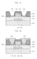
- FIGS. 8 to 18 are diagrams for illustrating a process sequence to fabricate a transistor device having an improved on/off proportion using the N-type chalcogenide material and the P-type chalcogenide material.
- a metal layer 202 for gate electrode is formed on a substrate 200, for example, a glass substrate ( FIG. 8 ).
- the metal layer 202 for gate electrode 202 is formed on the substrate 200 using a sputtering method.
- the metal layer for gate electrode 202 for example, is formed of a gold layer, an aluminum layer or a chrome layer.
- the metal layer for gate electrode 202 is patterned using a photolithography process to form a gate electrode 204. Therefore, the gate electrode 204 having a lower gate shape is completed ( FIG. 9 ).
- the gate electrode 204 serves to turn on/off optical current flowing on a chalcogenide layer 208 to be described later.
- a gate oxide 206 and the gate electrode 204 are constituted in a lower gate shape formed in a lower part of the chalcogenide layer 208, however, the gate oxide 206 and the gate electrode 204 may be constituted by an upper gate shape formed in the upper part of the chalcogenide layer 208.
- the gate oxide 206 is formed on the gate electrode 204 and the substrate 200 ( FIG. 10 ).
- the gate oxide 206 may be formed of chalcogonide oxide, for example, an As 2 S 3 layer, or organic material such as a polymer PMMA film, a silicon oxide film, a silicon insulating film or the like.
- the polymer poly methyl methacrylate (PMMA) layer which is organic material constituting the gate oxide 206, is made of a transparent layer material.
- the gate oxide 220 maintains a good contact with a chalcogenide layer 208 and serves not to change the characteristics of the chalcogenide layer 208 during the manufacturing process.
- the gate oxide 206 is formed by using a plasma enhanced chemical vapor deposition (PECVD) method.
- PECVD plasma enhanced chemical vapor deposition
- the amorphous chalcogenide layer 208 is deposited on the gate oxide 206.
- the argon gas and the oxygen gas are injected simultaneously into the deposition device in order to an amorphous N-type chalcogenide layer 208.
- some of the injected oxygen gas is injected into the deposited chalcogenide material, and, the N-type chalcogenide layer 208 is formed by means of the oxygen injected at this time.
- the chalcogenide layer 208 is formed as a GST layer using a sputtering method ( FIG. 11 ).
- the laser is emitted onto an upper surface of the amorphous chalcogenide layer 208 to a crystalline chalcogenide layer 209 ( FIG. 12 ).
- a diffusion prevention layer 210 is deposited on the chalcogenide layer 209 in order to prevent the diffusion.
- the diffusion prevention layer 210 is formed of a silicon oxide film SiO 2 or the like.
- a metal layer 212 is formed on the diffusion prevention layer 210.
- the metal layer 212 is formed using aluminum (A1) ( FIG. 13 ).
- the diffusion prevention layer 210 and the metal layer 212 formed on the crystalline chalcogenide layer 209 are patterned using a photolithography process and a wet-etching process to form a diffusion prevention layer 214 and a metal layer 216 having a predetermined width ( FIG. 14 ).
- the oxy-injected chalcogenide layer 209 is changed to have N-type conductivity material to P-type conductivity material using a method of depositing GeTe on the chalcogenide layer 209 and the metal layer 216 formed on the gate oxide 206 and performing annealing thereon to be diffused.
- the annealing temperature to be diffused is annealed at a temperature that the phase of chalcogenide is changed from amorphous to crystalline for about an hour.
- a GeTe thin film is diffused from both sides of the chalcogenide film 209 on which the diffusion prevention layer 214 is not formed through the annealing process.
- the GeTe thin film deposited on the exposed chalcogenide layer 209 is diffused from the both sides of the chalcogenide layer 209 having N-type conductivity through the annealing process. Therefore, the both sides of the chalcogenide layer 209 having N-type conductivity is changed into a chalcogenide layer 220 having P-type conductivity.
- the chalcogenide layer 209 on which the diffusion prevention layer 214 is formed that is, the non-exposed chalcogenide layer 209, maintains a state of the chalcogenide layer 218 having N-type conductivity, as it is.
- a process where a channel of transistor is naturally formed as described above will be referred to as a self-aligned channel process' ( FIG. 15 ).
- the width and length of a channel is naturally formed according to the shape of an oxidation prevention layer 214 patterned on the N-type chalcogenide layer 209.
- the GeTe deposited on the diffusion prevention layer 214 will be removed in the following process.
- the chalcogenide layer 220 having P-type conductivity is patterned to have a predetermined width ( FIG. 16 ).
- Layers 222 are formed on the chalcogenide layer 220, the metal layer 216, and the gate oxide 206 to allow contact holes 224 to be formed ( FIG. 17 ).
- a source-side metal electrode 226 and a drain-side metal electrode 228 are formed on the contact holes 224, thereby completing a thin film transistor ( FIG. 18 ).
- FIG. 19 shows a shape of a device manufactured according to the process sequence shown in FIGS. 8 to 17 .
- FIG. 19 shows a shape right before source-side and drain-side metal electrodes are formed.
- a portion in the central portion, indicated in black, corresponds to a channel of transistor.
- the thin film transistor according to the present invention has an advantage that a width of channel is naturally aligned through a self-aligned channel process as mentioned with reference to FIG. 15 .
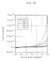
- FIG. 20 is a graph illustrating properties of a doped homojunction chalcogenide thin film transistor fabricated using the N-type chalcogenide and P-type chalcogenide manufactured through the process as described above.
- An axis X represents source-drain voltage
- an axis Y represents ampere drain current.
Landscapes
- Thin Film Transistor (AREA)
- Physical Deposition Of Substances That Are Components Of Semiconductor Devices (AREA)
- Physical Vapour Deposition (AREA)
- Semiconductor Memories (AREA)
Applications Claiming Priority (2)
| Application Number | Priority Date | Filing Date | Title |
|---|---|---|---|
| KR20070126333 | 2007-12-06 | ||
| KR1020080114541A KR101175189B1 (ko) | 2007-12-06 | 2008-11-18 | N형 및 p형 칼코제나이드 소재 제조 방법, 칼코제나이드 박막형 트랜지스터 및 그의 제작 방법 |
Publications (3)
| Publication Number | Publication Date |
|---|---|
| EP2068368A2 true EP2068368A2 (fr) | 2009-06-10 |
| EP2068368A3 EP2068368A3 (fr) | 2009-08-05 |
| EP2068368B1 EP2068368B1 (fr) | 2012-10-10 |
Family
ID=40407861
Family Applications (1)
| Application Number | Title | Priority Date | Filing Date |
|---|---|---|---|
| EP08170842A Not-in-force EP2068368B1 (fr) | 2007-12-06 | 2008-12-05 | Procédé de fabrication d'un transistor à couche mince de chalcogénure de type N et de type P |
Country Status (3)
| Country | Link |
|---|---|
| US (1) | US8039926B2 (fr) |
| EP (1) | EP2068368B1 (fr) |
| JP (1) | JP5102191B2 (fr) |
Cited By (9)
| Publication number | Priority date | Publication date | Assignee | Title |
|---|---|---|---|---|
| TWI400542B (zh) * | 2009-10-08 | 2013-07-01 | Chunghwa Picture Tubes Ltd | 半穿透半反射式薄膜電晶體面板及其製造方法 |
| US9245742B2 (en) | 2013-12-18 | 2016-01-26 | Asm Ip Holding B.V. | Sulfur-containing thin films |
| US9461134B1 (en) | 2015-05-20 | 2016-10-04 | Asm Ip Holding B.V. | Method for forming source/drain contact structure with chalcogen passivation |
| US9478419B2 (en) | 2013-12-18 | 2016-10-25 | Asm Ip Holding B.V. | Sulfur-containing thin films |
| US9711396B2 (en) | 2015-06-16 | 2017-07-18 | Asm Ip Holding B.V. | Method for forming metal chalcogenide thin films on a semiconductor device |
| US9711350B2 (en) | 2015-06-03 | 2017-07-18 | Asm Ip Holding B.V. | Methods for semiconductor passivation by nitridation |
| US9741815B2 (en) | 2015-06-16 | 2017-08-22 | Asm Ip Holding B.V. | Metal selenide and metal telluride thin films for semiconductor device applications |
| US10490475B2 (en) | 2015-06-03 | 2019-11-26 | Asm Ip Holding B.V. | Methods for semiconductor passivation by nitridation after oxide removal |
| WO2020060891A1 (fr) * | 2018-09-21 | 2020-03-26 | Qualcomm Incorporated | Circuits à semi-conducteur à oxyde de métal complémentaire (cmos) à transistor à couches minces (tft) flexible à double grille et procédés de fabrication associés |
Families Citing this family (16)
| Publication number | Priority date | Publication date | Assignee | Title |
|---|---|---|---|---|
| US7883931B2 (en) * | 2008-02-06 | 2011-02-08 | Micron Technology, Inc. | Methods of forming memory cells, and methods of forming programmed memory cells |
| EP2497123A2 (fr) * | 2009-11-05 | 2012-09-12 | Dow Global Technologies LLC | Fabrication de compositions de chalcogénure de type n et leurs utilisations dans des dispositifs photovoltaïques |
| KR101701920B1 (ko) * | 2010-03-05 | 2017-02-03 | 삼성전자주식회사 | 포토다이오드 및 이의 제조 방법, 이를 이용한 광전 소자 |
| KR102144999B1 (ko) * | 2013-11-05 | 2020-08-14 | 삼성전자주식회사 | 이차원 물질과 그 형성방법 및 이차원 물질을 포함하는 소자 |
| SG11201606376WA (en) * | 2014-03-21 | 2016-09-29 | Intel Corp | Transition metal dichalcogenide semiconductor assemblies |
| US10217819B2 (en) * | 2015-05-20 | 2019-02-26 | Samsung Electronics Co., Ltd. | Semiconductor device including metal-2 dimensional material-semiconductor contact |
| US10026751B2 (en) | 2015-10-02 | 2018-07-17 | Samsung Electronics Co., Ltd. | Semiconductor device including a repeater/buffer at higher metal routing layers and methods of manufacturing the same |
| JP7048182B2 (ja) * | 2016-08-26 | 2022-04-05 | インテル・コーポレーション | 集積回路のデバイス構造及び両面製造技術 |
| US10854591B2 (en) | 2016-11-04 | 2020-12-01 | Samsung Electronics Co., Ltd. | Semiconductor device including a repeater/buffer at upper metal routing layers and methods of manufacturing the same |
| US10811254B2 (en) | 2017-08-29 | 2020-10-20 | Electronics And Telecommunications Research Institute | Method for fabricating metal chalcogenide thin films |
| KR101874258B1 (ko) * | 2017-10-19 | 2018-08-02 | 경희대학교 산학협력단 | 전이금속 디칼코게나이드 박막 및 그 제조방법 |
| US11888034B2 (en) * | 2019-06-07 | 2024-01-30 | Intel Corporation | Transistors with metal chalcogenide channel materials |
| US11777029B2 (en) | 2019-06-27 | 2023-10-03 | Intel Corporation | Vertical transistors for ultra-dense logic and memory applications |
| US11171243B2 (en) | 2019-06-27 | 2021-11-09 | Intel Corporation | Transistor structures with a metal oxide contact buffer |
| CN111180524B (zh) * | 2020-01-21 | 2023-04-18 | 合肥鑫晟光电科技有限公司 | 薄膜晶体管、显示面板及其制备方法、显示装置 |
| US12266720B2 (en) | 2020-12-21 | 2025-04-01 | Intel Corporation | Transistors with monocrystalline metal chalcogenide channel materials |
Family Cites Families (11)
| Publication number | Priority date | Publication date | Assignee | Title |
|---|---|---|---|---|
| US3983076A (en) * | 1973-07-02 | 1976-09-28 | Energy Conversion Devices, Inc. | N-type amorphous semiconductor materials |
| JPS58186961A (ja) | 1982-04-26 | 1983-11-01 | Toshiba Corp | 半導体装置 |
| JPS5988869A (ja) | 1982-11-12 | 1984-05-22 | Toshiba Corp | 半導体装置 |
| JPS63161672A (ja) | 1986-12-25 | 1988-07-05 | Toshiba Corp | 有機薄膜素子 |
| US6709958B2 (en) | 2001-08-30 | 2004-03-23 | Micron Technology, Inc. | Integrated circuit device and fabrication using metal-doped chalcogenide materials |
| JP4470398B2 (ja) | 2003-06-23 | 2010-06-02 | Tdk株式会社 | 電界効果トランジスタ |
| US7893419B2 (en) | 2003-08-04 | 2011-02-22 | Intel Corporation | Processing phase change material to improve programming speed |
| JP4425878B2 (ja) * | 2005-10-31 | 2010-03-03 | 韓國電子通信研究院 | カルコゲナイド系元素を含む光伝導層を有するフォト薄膜トランジスタ及びこれを用いたイメージセンサの単位セル |
| KR101225372B1 (ko) | 2005-12-29 | 2013-01-22 | 엘지디스플레이 주식회사 | 박막트랜지스터 및 그 제조방법과 그 박막트랜지스터를포함하는 평판 표시 장치 |
| GB2437768A (en) * | 2006-05-03 | 2007-11-07 | Seiko Epson Corp | Photosensing TFT |
| US20080083924A1 (en) | 2006-10-09 | 2008-04-10 | Kibong Song | Thin film transistor having chalcogenide layer and method of fabricating the thin film transistor |
-
2008
- 2008-12-05 EP EP08170842A patent/EP2068368B1/fr not_active Not-in-force
- 2008-12-05 US US12/328,933 patent/US8039926B2/en not_active Expired - Fee Related
- 2008-12-08 JP JP2008312341A patent/JP5102191B2/ja not_active Expired - Fee Related
Cited By (13)
| Publication number | Priority date | Publication date | Assignee | Title |
|---|---|---|---|---|
| TWI400542B (zh) * | 2009-10-08 | 2013-07-01 | Chunghwa Picture Tubes Ltd | 半穿透半反射式薄膜電晶體面板及其製造方法 |
| US9721786B2 (en) | 2013-12-18 | 2017-08-01 | Asm Ip Holding B.V. | Sulfur-containing thin films |
| US9478419B2 (en) | 2013-12-18 | 2016-10-25 | Asm Ip Holding B.V. | Sulfur-containing thin films |
| US9245742B2 (en) | 2013-12-18 | 2016-01-26 | Asm Ip Holding B.V. | Sulfur-containing thin films |
| US10199213B2 (en) | 2013-12-18 | 2019-02-05 | Asm Ip Holding B.V. | Sulfur-containing thin films |
| US10553424B2 (en) | 2013-12-18 | 2020-02-04 | Asm Ip Holding B.V. | Sulfur-containing thin films |
| US10854444B2 (en) | 2013-12-18 | 2020-12-01 | Asm Ip Holding B.V. | Sulfur-containing thin films |
| US9461134B1 (en) | 2015-05-20 | 2016-10-04 | Asm Ip Holding B.V. | Method for forming source/drain contact structure with chalcogen passivation |
| US9711350B2 (en) | 2015-06-03 | 2017-07-18 | Asm Ip Holding B.V. | Methods for semiconductor passivation by nitridation |
| US10490475B2 (en) | 2015-06-03 | 2019-11-26 | Asm Ip Holding B.V. | Methods for semiconductor passivation by nitridation after oxide removal |
| US9711396B2 (en) | 2015-06-16 | 2017-07-18 | Asm Ip Holding B.V. | Method for forming metal chalcogenide thin films on a semiconductor device |
| US9741815B2 (en) | 2015-06-16 | 2017-08-22 | Asm Ip Holding B.V. | Metal selenide and metal telluride thin films for semiconductor device applications |
| WO2020060891A1 (fr) * | 2018-09-21 | 2020-03-26 | Qualcomm Incorporated | Circuits à semi-conducteur à oxyde de métal complémentaire (cmos) à transistor à couches minces (tft) flexible à double grille et procédés de fabrication associés |
Also Published As
| Publication number | Publication date |
|---|---|
| EP2068368B1 (fr) | 2012-10-10 |
| US8039926B2 (en) | 2011-10-18 |
| US20090146141A1 (en) | 2009-06-11 |
| JP2009138273A (ja) | 2009-06-25 |
| EP2068368A3 (fr) | 2009-08-05 |
| JP5102191B2 (ja) | 2012-12-19 |
Similar Documents
| Publication | Publication Date | Title |
|---|---|---|
| US8039926B2 (en) | Method for manufacturing N-type and P-type chalcogenide material, doped homojunction chalcogenide thin film transistor and method of fabricating the same | |
| Shim et al. | TFT channel materials for display applications: From amorphous silicon to transition metal dichalcogenides | |
| US20080083924A1 (en) | Thin film transistor having chalcogenide layer and method of fabricating the thin film transistor | |
| JP4919811B2 (ja) | ドープされた部分を有する堆積チャネル領域を含むトランジスタ | |
| US9123817B2 (en) | Transistors and electronic devices including the same | |
| US20110149645A1 (en) | Multi-level programmable pcram memory | |
| US6984552B2 (en) | Method for doping semiconductor layer, method for producing thin film semiconductor element and thin film semiconductor element | |
| US8324628B2 (en) | Channel layer for a thin film transistor, thin film transistor including the same, and methods of manufacturing the same | |
| US7915101B2 (en) | Thin film transistor and organic light emitting display using the same | |
| KR101552975B1 (ko) | 산화물 반도체 및 이를 포함하는 박막 트랜지스터 | |
| JP2008199005A (ja) | 薄膜トランジスタ及びその製造方法 | |
| US20120025187A1 (en) | Transistors, methods of manufacturing transistors, and electronic devices including transistors | |
| JP2005268724A (ja) | 電子素子およびその製造方法 | |
| US20120126223A1 (en) | Transistors, methods of manufacturing the same and electronic devices including transistors | |
| Reo et al. | Molecular Doping Enabling Mobility Boosting of 2D Sn2+‐Based Perovskites | |
| CN113571533A (zh) | 阵列基板及显示面板 | |
| KR20210089452A (ko) | 박막 트랜지스터 광 센서 및 이의 제조방법 | |
| KR102060377B1 (ko) | 디스플레이 소자, 그 제조 방법, 및 이미지 센서 소자의 제조방법 | |
| KR101175189B1 (ko) | N형 및 p형 칼코제나이드 소재 제조 방법, 칼코제나이드 박막형 트랜지스터 및 그의 제작 방법 | |
| KR102420428B1 (ko) | 산화물 반도체 기반의 p-n 접합을 이용한 반도체 소자, 이의 제조방법 및 이를 포함하는 광 검출기 | |
| Kang et al. | Investigation of sub-stoichiometric MoOx hole-selective contacts for rear junction passivating contact silicon solar cells | |
| US20070190721A1 (en) | Semiconductor memory device having an alloy metal gate electrode and method of manufacturing the same | |
| Kim et al. | Transparent, Multivalued Transistors Enabled By Area‐Selective Optical Doping on Ga‐Doped IZTO Thin Films | |
| KR102231372B1 (ko) | 산화물 반도체 박막 트랜지스터 및 이의 제조방법 | |
| US7851791B2 (en) | Thin film transistor having N-type and P-type CIS thin films and method of manufacturing the same |
Legal Events
| Date | Code | Title | Description |
|---|---|---|---|
| PUAI | Public reference made under article 153(3) epc to a published international application that has entered the european phase |
Free format text: ORIGINAL CODE: 0009012 |
|
| AK | Designated contracting states |
Kind code of ref document: A2 Designated state(s): AT BE BG CH CY CZ DE DK EE ES FI FR GB GR HR HU IE IS IT LI LT LU LV MC MT NL NO PL PT RO SE SI SK TR |
|
| AX | Request for extension of the european patent |
Extension state: AL BA MK RS |
|
| PUAL | Search report despatched |
Free format text: ORIGINAL CODE: 0009013 |
|
| AK | Designated contracting states |
Kind code of ref document: A3 Designated state(s): AT BE BG CH CY CZ DE DK EE ES FI FR GB GR HR HU IE IS IT LI LT LU LV MC MT NL NO PL PT RO SE SI SK TR |
|
| AX | Request for extension of the european patent |
Extension state: AL BA MK RS |
|
| 17P | Request for examination filed |
Effective date: 20100205 |
|
| 17Q | First examination report despatched |
Effective date: 20100301 |
|
| AKX | Designation fees paid |
Designated state(s): AT BE BG CH CY CZ DE DK EE ES FI FR GB GR HR HU IE IS IT LI LT LU LV MC MT NL NO PL PT RO SE SI SK TR |
|
| RIC1 | Information provided on ipc code assigned before grant |
Ipc: H01L 29/786 20060101AFI20120418BHEP Ipc: H01L 29/24 20060101ALI20120418BHEP Ipc: H01L 29/66 20060101ALI20120418BHEP |
|
| RTI1 | Title (correction) |
Free format text: METHOD FOR MANUFACTURING N-TYPE AND P-TYPE CHALCOGENIDE THIN FILM TRANSISTOR |
|
| GRAP | Despatch of communication of intention to grant a patent |
Free format text: ORIGINAL CODE: EPIDOSNIGR1 |
|
| GRAS | Grant fee paid |
Free format text: ORIGINAL CODE: EPIDOSNIGR3 |
|
| GRAA | (expected) grant |
Free format text: ORIGINAL CODE: 0009210 |
|
| AK | Designated contracting states |
Kind code of ref document: B1 Designated state(s): AT BE BG CH CY CZ DE DK EE ES FI FR GB GR HR HU IE IS IT LI LT LU LV MC MT NL NO PL PT RO SE SI SK TR |
|
| REG | Reference to a national code |
Ref country code: GB Ref legal event code: FG4D |
|
| REG | Reference to a national code |
Ref country code: AT Ref legal event code: REF Ref document number: 579302 Country of ref document: AT Kind code of ref document: T Effective date: 20121015 Ref country code: CH Ref legal event code: EP |
|
| REG | Reference to a national code |
Ref country code: IE Ref legal event code: FG4D |
|
| REG | Reference to a national code |
Ref country code: DE Ref legal event code: R096 Ref document number: 602008019257 Country of ref document: DE Effective date: 20121206 |
|
| PG25 | Lapsed in a contracting state [announced via postgrant information from national office to epo] |
Ref country code: SI Free format text: LAPSE BECAUSE OF FAILURE TO SUBMIT A TRANSLATION OF THE DESCRIPTION OR TO PAY THE FEE WITHIN THE PRESCRIBED TIME-LIMIT Effective date: 20121010 |
|
| REG | Reference to a national code |
Ref country code: NL Ref legal event code: VDEP Effective date: 20121010 |
|
| REG | Reference to a national code |
Ref country code: AT Ref legal event code: MK05 Ref document number: 579302 Country of ref document: AT Kind code of ref document: T Effective date: 20121010 |
|
| REG | Reference to a national code |
Ref country code: LT Ref legal event code: MG4D |
|
| PG25 | Lapsed in a contracting state [announced via postgrant information from national office to epo] |
Ref country code: ES Free format text: LAPSE BECAUSE OF FAILURE TO SUBMIT A TRANSLATION OF THE DESCRIPTION OR TO PAY THE FEE WITHIN THE PRESCRIBED TIME-LIMIT Effective date: 20130121 Ref country code: HR Free format text: LAPSE BECAUSE OF FAILURE TO SUBMIT A TRANSLATION OF THE DESCRIPTION OR TO PAY THE FEE WITHIN THE PRESCRIBED TIME-LIMIT Effective date: 20121010 Ref country code: LT Free format text: LAPSE BECAUSE OF FAILURE TO SUBMIT A TRANSLATION OF THE DESCRIPTION OR TO PAY THE FEE WITHIN THE PRESCRIBED TIME-LIMIT Effective date: 20121010 Ref country code: FI Free format text: LAPSE BECAUSE OF FAILURE TO SUBMIT A TRANSLATION OF THE DESCRIPTION OR TO PAY THE FEE WITHIN THE PRESCRIBED TIME-LIMIT Effective date: 20121010 Ref country code: NL Free format text: LAPSE BECAUSE OF FAILURE TO SUBMIT A TRANSLATION OF THE DESCRIPTION OR TO PAY THE FEE WITHIN THE PRESCRIBED TIME-LIMIT Effective date: 20121010 Ref country code: SE Free format text: LAPSE BECAUSE OF FAILURE TO SUBMIT A TRANSLATION OF THE DESCRIPTION OR TO PAY THE FEE WITHIN THE PRESCRIBED TIME-LIMIT Effective date: 20121010 Ref country code: IS Free format text: LAPSE BECAUSE OF FAILURE TO SUBMIT A TRANSLATION OF THE DESCRIPTION OR TO PAY THE FEE WITHIN THE PRESCRIBED TIME-LIMIT Effective date: 20130210 Ref country code: NO Free format text: LAPSE BECAUSE OF FAILURE TO SUBMIT A TRANSLATION OF THE DESCRIPTION OR TO PAY THE FEE WITHIN THE PRESCRIBED TIME-LIMIT Effective date: 20130110 |
|
| PG25 | Lapsed in a contracting state [announced via postgrant information from national office to epo] |
Ref country code: BE Free format text: LAPSE BECAUSE OF FAILURE TO SUBMIT A TRANSLATION OF THE DESCRIPTION OR TO PAY THE FEE WITHIN THE PRESCRIBED TIME-LIMIT Effective date: 20121010 Ref country code: PT Free format text: LAPSE BECAUSE OF FAILURE TO SUBMIT A TRANSLATION OF THE DESCRIPTION OR TO PAY THE FEE WITHIN THE PRESCRIBED TIME-LIMIT Effective date: 20130211 Ref country code: CY Free format text: LAPSE BECAUSE OF FAILURE TO SUBMIT A TRANSLATION OF THE DESCRIPTION OR TO PAY THE FEE WITHIN THE PRESCRIBED TIME-LIMIT Effective date: 20121010 Ref country code: LV Free format text: LAPSE BECAUSE OF FAILURE TO SUBMIT A TRANSLATION OF THE DESCRIPTION OR TO PAY THE FEE WITHIN THE PRESCRIBED TIME-LIMIT Effective date: 20121010 Ref country code: GR Free format text: LAPSE BECAUSE OF FAILURE TO SUBMIT A TRANSLATION OF THE DESCRIPTION OR TO PAY THE FEE WITHIN THE PRESCRIBED TIME-LIMIT Effective date: 20130111 Ref country code: PL Free format text: LAPSE BECAUSE OF FAILURE TO SUBMIT A TRANSLATION OF THE DESCRIPTION OR TO PAY THE FEE WITHIN THE PRESCRIBED TIME-LIMIT Effective date: 20121010 |
|
| PG25 | Lapsed in a contracting state [announced via postgrant information from national office to epo] |
Ref country code: AT Free format text: LAPSE BECAUSE OF FAILURE TO SUBMIT A TRANSLATION OF THE DESCRIPTION OR TO PAY THE FEE WITHIN THE PRESCRIBED TIME-LIMIT Effective date: 20121010 |
|
| PG25 | Lapsed in a contracting state [announced via postgrant information from national office to epo] |
Ref country code: CZ Free format text: LAPSE BECAUSE OF FAILURE TO SUBMIT A TRANSLATION OF THE DESCRIPTION OR TO PAY THE FEE WITHIN THE PRESCRIBED TIME-LIMIT Effective date: 20121010 Ref country code: MC Free format text: LAPSE BECAUSE OF NON-PAYMENT OF DUE FEES Effective date: 20121231 Ref country code: DK Free format text: LAPSE BECAUSE OF FAILURE TO SUBMIT A TRANSLATION OF THE DESCRIPTION OR TO PAY THE FEE WITHIN THE PRESCRIBED TIME-LIMIT Effective date: 20121010 Ref country code: BG Free format text: LAPSE BECAUSE OF FAILURE TO SUBMIT A TRANSLATION OF THE DESCRIPTION OR TO PAY THE FEE WITHIN THE PRESCRIBED TIME-LIMIT Effective date: 20130110 Ref country code: EE Free format text: LAPSE BECAUSE OF FAILURE TO SUBMIT A TRANSLATION OF THE DESCRIPTION OR TO PAY THE FEE WITHIN THE PRESCRIBED TIME-LIMIT Effective date: 20121010 Ref country code: SK Free format text: LAPSE BECAUSE OF FAILURE TO SUBMIT A TRANSLATION OF THE DESCRIPTION OR TO PAY THE FEE WITHIN THE PRESCRIBED TIME-LIMIT Effective date: 20121010 |
|
| REG | Reference to a national code |
Ref country code: CH Ref legal event code: PL |
|
| PLBE | No opposition filed within time limit |
Free format text: ORIGINAL CODE: 0009261 |
|
| STAA | Information on the status of an ep patent application or granted ep patent |
Free format text: STATUS: NO OPPOSITION FILED WITHIN TIME LIMIT |
|
| PG25 | Lapsed in a contracting state [announced via postgrant information from national office to epo] |
Ref country code: IT Free format text: LAPSE BECAUSE OF FAILURE TO SUBMIT A TRANSLATION OF THE DESCRIPTION OR TO PAY THE FEE WITHIN THE PRESCRIBED TIME-LIMIT Effective date: 20121010 Ref country code: RO Free format text: LAPSE BECAUSE OF FAILURE TO SUBMIT A TRANSLATION OF THE DESCRIPTION OR TO PAY THE FEE WITHIN THE PRESCRIBED TIME-LIMIT Effective date: 20121010 |
|
| 26N | No opposition filed |
Effective date: 20130711 |
|
| GBPC | Gb: european patent ceased through non-payment of renewal fee |
Effective date: 20130110 |
|
| REG | Reference to a national code |
Ref country code: IE Ref legal event code: MM4A |
|
| REG | Reference to a national code |
Ref country code: FR Ref legal event code: ST Effective date: 20130830 |
|
| PG25 | Lapsed in a contracting state [announced via postgrant information from national office to epo] |
Ref country code: IE Free format text: LAPSE BECAUSE OF NON-PAYMENT OF DUE FEES Effective date: 20121205 Ref country code: CH Free format text: LAPSE BECAUSE OF NON-PAYMENT OF DUE FEES Effective date: 20121231 Ref country code: LI Free format text: LAPSE BECAUSE OF NON-PAYMENT OF DUE FEES Effective date: 20121231 |
|
| REG | Reference to a national code |
Ref country code: DE Ref legal event code: R097 Ref document number: 602008019257 Country of ref document: DE Effective date: 20130711 |
|
| PG25 | Lapsed in a contracting state [announced via postgrant information from national office to epo] |
Ref country code: MT Free format text: LAPSE BECAUSE OF FAILURE TO SUBMIT A TRANSLATION OF THE DESCRIPTION OR TO PAY THE FEE WITHIN THE PRESCRIBED TIME-LIMIT Effective date: 20121010 Ref country code: FR Free format text: LAPSE BECAUSE OF NON-PAYMENT OF DUE FEES Effective date: 20130102 Ref country code: GB Free format text: LAPSE BECAUSE OF NON-PAYMENT OF DUE FEES Effective date: 20130110 |
|
| PGFP | Annual fee paid to national office [announced via postgrant information from national office to epo] |
Ref country code: DE Payment date: 20131121 Year of fee payment: 6 |
|
| PG25 | Lapsed in a contracting state [announced via postgrant information from national office to epo] |
Ref country code: TR Free format text: LAPSE BECAUSE OF FAILURE TO SUBMIT A TRANSLATION OF THE DESCRIPTION OR TO PAY THE FEE WITHIN THE PRESCRIBED TIME-LIMIT Effective date: 20121010 |
|
| PG25 | Lapsed in a contracting state [announced via postgrant information from national office to epo] |
Ref country code: LU Free format text: LAPSE BECAUSE OF NON-PAYMENT OF DUE FEES Effective date: 20121205 |
|
| PG25 | Lapsed in a contracting state [announced via postgrant information from national office to epo] |
Ref country code: HU Free format text: LAPSE BECAUSE OF FAILURE TO SUBMIT A TRANSLATION OF THE DESCRIPTION OR TO PAY THE FEE WITHIN THE PRESCRIBED TIME-LIMIT Effective date: 20081205 |
|
| REG | Reference to a national code |
Ref country code: DE Ref legal event code: R119 Ref document number: 602008019257 Country of ref document: DE |
|
| PG25 | Lapsed in a contracting state [announced via postgrant information from national office to epo] |
Ref country code: DE Free format text: LAPSE BECAUSE OF NON-PAYMENT OF DUE FEES Effective date: 20150701 |