EP2068603A2 - Fixation d'amortissement de composant électronique élevé - Google Patents
Fixation d'amortissement de composant électronique élevé Download PDFInfo
- Publication number
- EP2068603A2 EP2068603A2 EP08163498A EP08163498A EP2068603A2 EP 2068603 A2 EP2068603 A2 EP 2068603A2 EP 08163498 A EP08163498 A EP 08163498A EP 08163498 A EP08163498 A EP 08163498A EP 2068603 A2 EP2068603 A2 EP 2068603A2
- Authority
- EP
- European Patent Office
- Prior art keywords
- electronic component
- dampening
- electronic
- circuit substrate
- dampening member
- Prior art date
- Legal status (The legal status is an assumption and is not a legal conclusion. Google has not performed a legal analysis and makes no representation as to the accuracy of the status listed.)
- Withdrawn
Links
Images
Classifications
-
- H—ELECTRICITY
- H05—ELECTRIC TECHNIQUES NOT OTHERWISE PROVIDED FOR
- H05K—PRINTED CIRCUITS; CASINGS OR CONSTRUCTIONAL DETAILS OF ELECTRIC APPARATUS; MANUFACTURE OF ASSEMBLAGES OF ELECTRICAL COMPONENTS
- H05K3/00—Apparatus or processes for manufacturing printed circuits
- H05K3/30—Assembling printed circuits with electric components, e.g. with resistors
- H05K3/301—Assembling printed circuits with electric components, e.g. with resistors by means of a mounting structure
-
- H—ELECTRICITY
- H05—ELECTRIC TECHNIQUES NOT OTHERWISE PROVIDED FOR
- H05K—PRINTED CIRCUITS; CASINGS OR CONSTRUCTIONAL DETAILS OF ELECTRIC APPARATUS; MANUFACTURE OF ASSEMBLAGES OF ELECTRICAL COMPONENTS
- H05K2201/00—Indexing scheme relating to printed circuits covered by H05K1/00
- H05K2201/01—Dielectrics
- H05K2201/0104—Properties and characteristics in general
- H05K2201/0133—Elastomeric or compliant polymer
-
- H—ELECTRICITY
- H05—ELECTRIC TECHNIQUES NOT OTHERWISE PROVIDED FOR
- H05K—PRINTED CIRCUITS; CASINGS OR CONSTRUCTIONAL DETAILS OF ELECTRIC APPARATUS; MANUFACTURE OF ASSEMBLAGES OF ELECTRICAL COMPONENTS
- H05K2201/00—Indexing scheme relating to printed circuits covered by H05K1/00
- H05K2201/10—Details of components or other objects attached to or integrated in a printed circuit board
- H05K2201/10007—Types of components
- H05K2201/10015—Non-printed capacitor
-
- H—ELECTRICITY
- H05—ELECTRIC TECHNIQUES NOT OTHERWISE PROVIDED FOR
- H05K—PRINTED CIRCUITS; CASINGS OR CONSTRUCTIONAL DETAILS OF ELECTRIC APPARATUS; MANUFACTURE OF ASSEMBLAGES OF ELECTRICAL COMPONENTS
- H05K2201/00—Indexing scheme relating to printed circuits covered by H05K1/00
- H05K2201/10—Details of components or other objects attached to or integrated in a printed circuit board
- H05K2201/10227—Other objects, e.g. metallic pieces
- H05K2201/10295—Metallic connector elements partly mounted in a hole of the PCB
-
- H—ELECTRICITY
- H05—ELECTRIC TECHNIQUES NOT OTHERWISE PROVIDED FOR
- H05K—PRINTED CIRCUITS; CASINGS OR CONSTRUCTIONAL DETAILS OF ELECTRIC APPARATUS; MANUFACTURE OF ASSEMBLAGES OF ELECTRICAL COMPONENTS
- H05K2201/00—Indexing scheme relating to printed circuits covered by H05K1/00
- H05K2201/10—Details of components or other objects attached to or integrated in a printed circuit board
- H05K2201/10227—Other objects, e.g. metallic pieces
- H05K2201/10393—Clamping a component by an element or a set of elements
-
- H—ELECTRICITY
- H05—ELECTRIC TECHNIQUES NOT OTHERWISE PROVIDED FOR
- H05K—PRINTED CIRCUITS; CASINGS OR CONSTRUCTIONAL DETAILS OF ELECTRIC APPARATUS; MANUFACTURE OF ASSEMBLAGES OF ELECTRICAL COMPONENTS
- H05K2201/00—Indexing scheme relating to printed circuits covered by H05K1/00
- H05K2201/10—Details of components or other objects attached to or integrated in a printed circuit board
- H05K2201/10227—Other objects, e.g. metallic pieces
- H05K2201/10409—Screws
-
- H—ELECTRICITY
- H05—ELECTRIC TECHNIQUES NOT OTHERWISE PROVIDED FOR
- H05K—PRINTED CIRCUITS; CASINGS OR CONSTRUCTIONAL DETAILS OF ELECTRIC APPARATUS; MANUFACTURE OF ASSEMBLAGES OF ELECTRICAL COMPONENTS
- H05K2201/00—Indexing scheme relating to printed circuits covered by H05K1/00
- H05K2201/10—Details of components or other objects attached to or integrated in a printed circuit board
- H05K2201/10431—Details of mounted components
- H05K2201/10583—Cylindrically shaped component; Fixing means therefore
-
- H—ELECTRICITY
- H05—ELECTRIC TECHNIQUES NOT OTHERWISE PROVIDED FOR
- H05K—PRINTED CIRCUITS; CASINGS OR CONSTRUCTIONAL DETAILS OF ELECTRIC APPARATUS; MANUFACTURE OF ASSEMBLAGES OF ELECTRICAL COMPONENTS
- H05K2201/00—Indexing scheme relating to printed circuits covered by H05K1/00
- H05K2201/10—Details of components or other objects attached to or integrated in a printed circuit board
- H05K2201/10613—Details of electrical connections of non-printed components, e.g. special leads
- H05K2201/10954—Other details of electrical connections
- H05K2201/10969—Metallic case or integral heatsink of component electrically connected to a pad on PCB
-
- H—ELECTRICITY
- H05—ELECTRIC TECHNIQUES NOT OTHERWISE PROVIDED FOR
- H05K—PRINTED CIRCUITS; CASINGS OR CONSTRUCTIONAL DETAILS OF ELECTRIC APPARATUS; MANUFACTURE OF ASSEMBLAGES OF ELECTRICAL COMPONENTS
- H05K2201/00—Indexing scheme relating to printed circuits covered by H05K1/00
- H05K2201/20—Details of printed circuits not provided for in H05K2201/01 - H05K2201/10
- H05K2201/2045—Protection against vibrations
-
- H—ELECTRICITY
- H05—ELECTRIC TECHNIQUES NOT OTHERWISE PROVIDED FOR
- H05K—PRINTED CIRCUITS; CASINGS OR CONSTRUCTIONAL DETAILS OF ELECTRIC APPARATUS; MANUFACTURE OF ASSEMBLAGES OF ELECTRICAL COMPONENTS
- H05K3/00—Apparatus or processes for manufacturing printed circuits
- H05K3/30—Assembling printed circuits with electric components, e.g. with resistors
- H05K3/32—Assembling printed circuits with electric components, e.g. with resistors electrically connecting electric components or wires to printed circuits
- H05K3/34—Assembling printed circuits with electric components, e.g. with resistors electrically connecting electric components or wires to printed circuits by soldering
- H05K3/3447—Lead-in-hole components
Definitions
- This invention relates to electronic assemblies having a large electronic component mounted to a circuit board, and more particularly to electronic assemblies subjected to a vibration environment.
- One technique for preventing damage and failure due to shock and/or vibration of an electronic assembly having a large electronic component soldered to a circuit substrate is to adhesively bond a surface of the electronic component to a housing or case for the assembly.
- This solution is not entirely satisfactory because adhesive materials have a coefficient of thermal expansion that is substantially different from the coefficient of thermal expansion of the body of the electronic component and substantially different from the coefficient of thermal expansion of the housing or other component to which the electronic component is adhesively bonded. These differences in coefficients of thermal expansion will cause the adhesive to expand and contract in response to temperature changes in a manner that is different from that of the other components of the assembly.
- the adhesive will tend to expand and contract at a different rate than the body of the electronic component and the body of the housing or other assembly component to which the body of the electronic component is adhered. These differences in the rates of expansion of the different materials will induce relative movement of the body of the electronic component with respect to the circuit substrate creating stresses on the solder joints. The stresses on the solder joints can result in cracking of the solder joints and failure of the electronic assembly. In addition, most adhesives tend to shrink during cure because of physical changes to the adhesive material, or contract after cooling down from the cure oven. These changes in geometry, can also cause stresses on solder joints and result in failure of the electronic assembly.
- Another technique for preventing damage and failure due to shock and/or vibration of an electronic assembly having a large electronic component soldered to a circuit substrate is to retain the large electronic component between opposite end plates welded or otherwise fixed to the body of the large electronic component and to the circuit substrate.
- the shock and/or vibration can often be sufficiently severe to cause the weld or other fixation to become broken, resulting in failure of the electronic assembly.
- the invention provides an improved electronic assembly in which an elastic dampening member and a clamping arrangement are utilized to stabilize an electronic component against lateral movement without imposing any substantial stresses on the solder joints.
- an electronic assembly includes a circuit substrate, an electronic component, an elastic dampening member, and a clamping member that compresses the dampening member between the clamping member and the electronic component.
- the dampening member has a top section engaging an upper surface of the electronic component and opposite end walls that extend downwardly from the top section of the dampening member and engage opposite sidewalls of the body of the electronic component. Further, in accordance with this aspect of the invention the clamping member urges the opposite end walls of the dampening member against the opposite sidewalls of the electronic component.
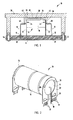
- FIG. 1 Shown in FIG. 1 is a cross-sectional view of an electronic assembly 10 employing a shock and/or vibration dampening structure in accordance with the invention.
- the assembly includes a circuit substrate 12 to which an electronic component 14 is mechanically attached and electrically connected by solder joints 15.
- Electronic component 14 includes a body 16 and electrical leads 18.
- circuit substrate 12 is provided with openings (not shown) for receiving the distal ends of leads 18, and contact pads 20.
- body 16 of electronic component 14 is also secured to circuit substrate 12 with supporting end plates 22 which are welded to opposite sidewalls 24 at weld joints 26 (as shown in FIG. 2 ).
- the bottom end or feet 28 of end plates 22 can be welded to circuit substrate 12, whereby electrical component 14 is securely affixed to circuit substrate 12 and exhibits some resistance to damage and failure upon repeated shock and vibration.
- securing electronic component 14 to circuit substrate 12 with end plates 22 does not always provide sufficient resistance to damage and failure of the electronic assembly when the assembly is subjected to severe shock and/or vibration of the type that is commonly encountered in automotive applications.
- electronic assembly 10 includes an elastic dampening member 30.
- Dampening member 30 includes a top section 32 that engages an upper surface 34 of body 16 of electronic component 14.
- Upper surface 34 of cylindrical body 16 (shown in FIGs. 1 and 2 ) refers generally to a surface area that faces upwardly in a direction away from circuit substrate 12 (i.e., a surface area opposite the surface area facing circuit substrate 12).
- Dampening member 30 also includes opposite end walls 36 that extend downwardly from top section 32 and engage opposite sidewalls 24 of body 16 of electronic component 14.
- Elastic dampening member 30 is sized and configured to fit snugly over body 16 electronic component 14 by slightly stretching elastic member 30, thereby providing an initial good grip of body 16 by elastic dampening member 30.
- a rigid clamping member 38 forcefully engages an upper surface of the opposite end walls 36, and thereby urges lower ends 40 of end walls 36 of dampening member 30 against the sidewalls 24 of the body 16 of electronic component 14. This can be accomplished for example by having the upper surfaces 42 of dampening member 30 atop end walls 36 sloped slightly toward each other (i.e., sloped toward top section 32).
- clamping member 38 is a housing member which may be secured to circuit substrate 12 with fasteners such as screws 44, such that housing member 38 together with circuit substrate 12 defines an enclosure to contain and/or provide a protective environment for electronic component 14 and/or other components mounted on or defined on circuit substrate 12.
- body 16 of electronic component 14 has a generally cylindrical shape and is fixed to circuit substrate 12 with the cylinder axis arranged parallel with the upper surface of circuit substrate 12 to which electronic component 14 is mounted.
- body 16 of electronic component 14 has a generally cylindrical shape and is fixed to circuit substrate 12 with the cylinder axis arranged parallel with the upper surface of circuit substrate 12 to which electronic component 14 is mounted.
- electronic components that may be stabilized against shock and vibration include capacitors (as illustrated), resistors, transistors, diodes, etc.
- the principles of the invention may be applied to stabilize any electronic component mounted to a circuit substrate against damage and failure due to shock and vibration, and is particularly applicable to larger or heavier (i.e., more massive) electronic components that acquire sufficient momentum during shock and vibration to transmit destructive forces through the electrical leads to solder joints on the circuit substrate.
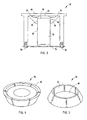
- FIG. 3 there is shown an alternative arrangement for an electronic assembly 50 having a cylindrical electronic component (e.g., a capacitor) mounted on a circuit substrate 54 with the cylindrical axis of the electronic component arranged perpendicular to the surface of circuit substrate 54 to which electronic component 52 is mounted.
- a cylindrical electronic component e.g., a capacitor
- an inverted cup-shaped dampening member 56 is fitted to the top end of electronic component 52.
- Dampening member 56 is an elastic material that is configured to be stretched to snugly fit over the top end 58 of electronic component 52, and as with dampening member 30 shown in FIGs. 1 and 2 , includes a top section 60 and end walls 62 that extend downwardly from top section 60 and engage the cylindrical sidewall of electronic component 52.
- a clamping member 64 engages upper surfaces 66 of dampening member 56, compressing end walls 62 downwardly and inwardly toward an upper surface area of cylindrical sidewall 68 of component 52, thereby forcefully engaging such surfaces at opposite wall surfaces, whereby the electronic component is securely gripped between opposite end walls 62 of dampening member 56, without exerting substantial force in the vertical direction while stabilizing component 52 against lateral movement when assembly 50 is subjected to shock and/or vibration.
- clamping member 64 may be a housing member secured to circuit substrate 54 with fasteners 70 (e.g., screws).
- dampening member 56 Details of dampening member 56 are illustrated in FIGs. 4 and 5 which show a top view and a bottom or underside view, respectively, of elastic dampening member 56.
- circuit substrates which may be employed with the invention encompass generally any printed circuit board or wiring board on which conductive traces may be defined and on which electronic components may be mounted or formed.
- the dampening members employed in the invention are elastic in the sense that they are relatively resiliently deformable as compared with the relatively more rigid clamping members or housing members.
- the elastic dampening members may comprise an elastomer (e.g., an elastic polymer), such as natural rubber, polyisoprene, butyl rubber, halogenated butyl rubbers, polybutadiene, styrene-butadiene rubber, nitrile rubber, hydrated nitrile rubber, chloroprene rubber, ethylene-propylene (EPM) rubber, ethylene-propylene-diene (EPDM) rubber, epichlorohydrin rubber, polyacrylic rubber, silicone rubber, fluorosilicone rubber, fluoroelastomers, perfluoroelastomers, polyether block amides, tetrafluoroethylene/propylene rubbers, chlorosulfonated polyethylene, ethylene-vinyl acetate, thermoplastic elastomers, thermoplastic vul
- an adhesive 80 may be disposed between surfaces of clamping member 38 and dampening member 30 to secure dampening member 30 to clamping member 38 and to prevent lateral (side-to-side) movement of dampening member 30 with respect to clamping member 38.
Landscapes
- Engineering & Computer Science (AREA)
- Manufacturing & Machinery (AREA)
- Microelectronics & Electronic Packaging (AREA)
- Structures For Mounting Electric Components On Printed Circuit Boards (AREA)
- Mounting Of Printed Circuit Boards And The Like (AREA)
- Connection Of Plates (AREA)
Applications Claiming Priority (1)
| Application Number | Priority Date | Filing Date | Title |
|---|---|---|---|
| US11/899,795 US20090067139A1 (en) | 2007-09-07 | 2007-09-07 | Large electronic component dampening fixation |
Publications (2)
| Publication Number | Publication Date |
|---|---|
| EP2068603A2 true EP2068603A2 (fr) | 2009-06-10 |
| EP2068603A3 EP2068603A3 (fr) | 2009-10-21 |
Family
ID=40431606
Family Applications (1)
| Application Number | Title | Priority Date | Filing Date |
|---|---|---|---|
| EP08163498A Withdrawn EP2068603A3 (fr) | 2007-09-07 | 2008-09-02 | Fixation d'amortissement de composant électronique élevé |
Country Status (2)
| Country | Link |
|---|---|
| US (1) | US20090067139A1 (fr) |
| EP (1) | EP2068603A3 (fr) |
Families Citing this family (5)
| Publication number | Priority date | Publication date | Assignee | Title |
|---|---|---|---|---|
| US20130271923A1 (en) * | 2012-04-13 | 2013-10-17 | Harvard Engineering Plc | Electrical apparatus |
| CN111682409B (zh) * | 2020-06-08 | 2022-04-26 | 江苏海潮电气科技有限公司 | 一种具有抗震防腐性能的组装式低压开关柜 |
| EP4102942A1 (fr) * | 2021-06-09 | 2022-12-14 | Veoneer Sweden AB | Structure d'assemblage d'alimentation de secours, unité de commande électronique et procédé de fabrication d'une structure d'assemblage d'alimentation de secours |
| KR20230163635A (ko) * | 2022-05-24 | 2023-12-01 | 주식회사 엘지에너지솔루션 | 심플 배터리팩 및 이의 제조방법 |
| CN119521523A (zh) * | 2023-08-23 | 2025-02-25 | 华为技术有限公司 | 电路板组件及电子设备 |
Family Cites Families (15)
| Publication number | Priority date | Publication date | Assignee | Title |
|---|---|---|---|---|
| JPS61324A (ja) * | 1985-01-12 | 1986-01-06 | 株式会社 日本コ−リン | 血圧測定装置 |
| US4974119A (en) * | 1988-09-14 | 1990-11-27 | The Charles Stark Draper Laboratories, Inc. | Conforming heat sink assembly |
| CA2165964C (fr) * | 1993-07-08 | 2005-03-15 | Curt Bruner | Architecture de systeme pour hdd |
| KR0126781Y1 (ko) * | 1994-08-23 | 1999-05-01 | 이형도 | 반도체소자 방열장치 |
| JPH08236962A (ja) * | 1995-02-22 | 1996-09-13 | Furukawa Electric Co Ltd:The | 電気部品を実装した基板の支持構造 |
| CA2151331A1 (fr) * | 1995-06-08 | 1996-12-09 | Henry W. C. Mok | Blindage contre les interferences electromagnetiques |
| US5754401A (en) * | 1996-02-16 | 1998-05-19 | Sun Microsystems, Inc. | Pressure compliantly protected heatsink for an electronic device |
| US6285078B1 (en) * | 1997-11-25 | 2001-09-04 | Intel Corporation | Thermal spreader cap and grease containment structure for semiconductor device |
| DE19929598C2 (de) * | 1999-06-28 | 2001-04-26 | Epcos Ag | Elektrolyt-Kondensator mit hoher Schwingbelastbarkeit |
| US6212074B1 (en) * | 2000-01-31 | 2001-04-03 | Sun Microsystems, Inc. | Apparatus for dissipating heat from a circuit board having a multilevel surface |
| US6243274B1 (en) * | 2000-04-20 | 2001-06-05 | Redcom Laboratories, Inc. | Shields for electronic components with ready access to shielded components |
| US6590278B1 (en) * | 2002-01-08 | 2003-07-08 | International Business Machines Corporation | Electronic package |
| US6631071B2 (en) * | 2002-01-16 | 2003-10-07 | Matsushita Electric Industrial Co., Ltd. | Capacitor module |
| US7023699B2 (en) * | 2002-06-10 | 2006-04-04 | Visteon Global Technologies, Inc. | Liquid cooled metal thermal stack for high-power dies |
| ATE452052T1 (de) * | 2007-05-21 | 2010-01-15 | Magneti Marelli Spa | Elektronische steuereinheit mit erweiterten blöcken |
-
2007
- 2007-09-07 US US11/899,795 patent/US20090067139A1/en not_active Abandoned
-
2008
- 2008-09-02 EP EP08163498A patent/EP2068603A3/fr not_active Withdrawn
Also Published As
| Publication number | Publication date |
|---|---|
| US20090067139A1 (en) | 2009-03-12 |
| EP2068603A3 (fr) | 2009-10-21 |
Similar Documents
| Publication | Publication Date | Title |
|---|---|---|
| CN107710892B (zh) | 电子控制装置 | |
| US5822193A (en) | Appparatus and method for rigidly stabilizing circuit boards | |
| US8331099B2 (en) | Method for fixing an electrical or an electronic component, particularly a printed-circuit board, in a housing and fixing element therefor | |
| CN101918246B (zh) | 控制装置外壳 | |
| US5909359A (en) | Apparatus for a circuit board extender | |
| US5402313A (en) | Electronic component heat sink attachment using a canted coil spring | |
| KR101688663B1 (ko) | 전력 반도체 모듈 | |
| US20090067139A1 (en) | Large electronic component dampening fixation | |
| US12436383B2 (en) | Vibration device | |
| US20100314147A1 (en) | Power tool | |
| US20030107874A1 (en) | De-mountable, solderless in-line lead module package with interface | |
| CN115279068A (zh) | 具有密封外壳的电子装置 | |
| US7575443B2 (en) | Combined fastening and contacting system for electrical components on superimposed circuit boards | |
| CN111902961B (zh) | 蓄电模块 | |
| WO2006015685A3 (fr) | Ensemble d'elements presentant une capacite de montage optimisee | |
| CN110461089B (zh) | 电子装置 | |
| US10830375B1 (en) | Flat electrical cable gripping tool | |
| JPS61187349A (ja) | 電力用半導体モジユール | |
| EP2070160B1 (fr) | Système de connexion scellé à courant élevé | |
| KR20210002337A (ko) | 전기 장비의 nvh 문제를 감소 또는 제거하도록 구성된 모듈 및 전기 장비 | |
| US5850104A (en) | Integral lid/clamp for high power transistor | |
| US6454587B1 (en) | Assembly for mounting a bus termination device to a printed circuit board (PCB) | |
| JP2021022715A (ja) | 回路基板、電源装置及び照明器具 | |
| US10959323B1 (en) | Over-torque protection features for mounting an electronic device to a heat dissipation object | |
| TWI915433B (zh) | 機械與電連接夾具及包含該機械與電連接夾具之電子系統 |
Legal Events
| Date | Code | Title | Description |
|---|---|---|---|
| PUAI | Public reference made under article 153(3) epc to a published international application that has entered the european phase |
Free format text: ORIGINAL CODE: 0009012 |
|
| AK | Designated contracting states |
Kind code of ref document: A2 Designated state(s): AT BE BG CH CY CZ DE DK EE ES FI FR GB GR HR HU IE IS IT LI LT LU LV MC MT NL NO PL PT RO SE SI SK TR |
|
| AX | Request for extension of the european patent |
Extension state: AL BA MK RS |
|
| PUAL | Search report despatched |
Free format text: ORIGINAL CODE: 0009013 |
|
| AK | Designated contracting states |
Kind code of ref document: A3 Designated state(s): AT BE BG CH CY CZ DE DK EE ES FI FR GB GR HR HU IE IS IT LI LT LU LV MC MT NL NO PL PT RO SE SI SK TR |
|
| AX | Request for extension of the european patent |
Extension state: AL BA MK RS |
|
| 17P | Request for examination filed |
Effective date: 20100421 |
|
| AKX | Designation fees paid |
Designated state(s): AT BE BG CH CY CZ DE DK EE ES FI FR GB GR HR HU IE IS IT LI LT LU LV MC MT NL NO PL PT RO SE SI SK TR |
|
| 17Q | First examination report despatched |
Effective date: 20100714 |
|
| STAA | Information on the status of an ep patent application or granted ep patent |
Free format text: STATUS: THE APPLICATION IS DEEMED TO BE WITHDRAWN |
|
| 18D | Application deemed to be withdrawn |
Effective date: 20101125 |