EP2070636A1 - Laserverarbeitungsverfahren - Google Patents
Laserverarbeitungsverfahren Download PDFInfo
- Publication number
- EP2070636A1 EP2070636A1 EP07828566A EP07828566A EP2070636A1 EP 2070636 A1 EP2070636 A1 EP 2070636A1 EP 07828566 A EP07828566 A EP 07828566A EP 07828566 A EP07828566 A EP 07828566A EP 2070636 A1 EP2070636 A1 EP 2070636A1
- Authority
- EP
- European Patent Office
- Prior art keywords
- laser light
- converging lens
- processing
- region
- converging
- Prior art date
- Legal status (The legal status is an assumption and is not a legal conclusion. Google has not performed a legal analysis and makes no representation as to the accuracy of the status listed.)
- Granted
Links
Images






Classifications
-
- B—PERFORMING OPERATIONS; TRANSPORTING
- B23—MACHINE TOOLS; METAL-WORKING NOT OTHERWISE PROVIDED FOR
- B23K—SOLDERING OR UNSOLDERING; WELDING; CLADDING OR PLATING BY SOLDERING OR WELDING; CUTTING BY APPLYING HEAT LOCALLY, e.g. FLAME CUTTING; WORKING BY LASER BEAM
- B23K26/00—Working by laser beam, e.g. welding, cutting or boring
- B23K26/02—Positioning or observing the workpiece, e.g. with respect to the point of impact; Aligning, aiming or focusing the laser beam
- B23K26/04—Automatically aligning, aiming or focusing the laser beam, e.g. using the back-scattered light
- B23K26/046—Automatically focusing the laser beam
- B23K26/048—Automatically focusing the laser beam by controlling the distance between laser head and workpiece
-
- B—PERFORMING OPERATIONS; TRANSPORTING
- B23—MACHINE TOOLS; METAL-WORKING NOT OTHERWISE PROVIDED FOR
- B23K—SOLDERING OR UNSOLDERING; WELDING; CLADDING OR PLATING BY SOLDERING OR WELDING; CUTTING BY APPLYING HEAT LOCALLY, e.g. FLAME CUTTING; WORKING BY LASER BEAM
- B23K26/00—Working by laser beam, e.g. welding, cutting or boring
- B23K26/36—Removing material
- B23K26/38—Removing material by boring or cutting
-
- B—PERFORMING OPERATIONS; TRANSPORTING
- B23—MACHINE TOOLS; METAL-WORKING NOT OTHERWISE PROVIDED FOR
- B23K—SOLDERING OR UNSOLDERING; WELDING; CLADDING OR PLATING BY SOLDERING OR WELDING; CUTTING BY APPLYING HEAT LOCALLY, e.g. FLAME CUTTING; WORKING BY LASER BEAM
- B23K26/00—Working by laser beam, e.g. welding, cutting or boring
- B23K26/02—Positioning or observing the workpiece, e.g. with respect to the point of impact; Aligning, aiming or focusing the laser beam
- B23K26/04—Automatically aligning, aiming or focusing the laser beam, e.g. using the back-scattered light
- B23K26/046—Automatically focusing the laser beam
-
- B—PERFORMING OPERATIONS; TRANSPORTING
- B23—MACHINE TOOLS; METAL-WORKING NOT OTHERWISE PROVIDED FOR
- B23K—SOLDERING OR UNSOLDERING; WELDING; CLADDING OR PLATING BY SOLDERING OR WELDING; CUTTING BY APPLYING HEAT LOCALLY, e.g. FLAME CUTTING; WORKING BY LASER BEAM
- B23K26/00—Working by laser beam, e.g. welding, cutting or boring
- B23K26/02—Positioning or observing the workpiece, e.g. with respect to the point of impact; Aligning, aiming or focusing the laser beam
- B23K26/06—Shaping the laser beam, e.g. by masks or multi-focusing
- B23K26/062—Shaping the laser beam, e.g. by masks or multi-focusing by direct control of the laser beam
-
- B—PERFORMING OPERATIONS; TRANSPORTING
- B23—MACHINE TOOLS; METAL-WORKING NOT OTHERWISE PROVIDED FOR
- B23K—SOLDERING OR UNSOLDERING; WELDING; CLADDING OR PLATING BY SOLDERING OR WELDING; CUTTING BY APPLYING HEAT LOCALLY, e.g. FLAME CUTTING; WORKING BY LASER BEAM
- B23K26/00—Working by laser beam, e.g. welding, cutting or boring
- B23K26/36—Removing material
- B23K26/40—Removing material taking account of the properties of the material involved
-
- B—PERFORMING OPERATIONS; TRANSPORTING
- B23—MACHINE TOOLS; METAL-WORKING NOT OTHERWISE PROVIDED FOR
- B23K—SOLDERING OR UNSOLDERING; WELDING; CLADDING OR PLATING BY SOLDERING OR WELDING; CUTTING BY APPLYING HEAT LOCALLY, e.g. FLAME CUTTING; WORKING BY LASER BEAM
- B23K26/00—Working by laser beam, e.g. welding, cutting or boring
- B23K26/36—Removing material
- B23K26/40—Removing material taking account of the properties of the material involved
- B23K26/402—Removing material taking account of the properties of the material involved involving non-metallic material, e.g. isolators
-
- B—PERFORMING OPERATIONS; TRANSPORTING
- B23—MACHINE TOOLS; METAL-WORKING NOT OTHERWISE PROVIDED FOR
- B23K—SOLDERING OR UNSOLDERING; WELDING; CLADDING OR PLATING BY SOLDERING OR WELDING; CUTTING BY APPLYING HEAT LOCALLY, e.g. FLAME CUTTING; WORKING BY LASER BEAM
- B23K26/00—Working by laser beam, e.g. welding, cutting or boring
- B23K26/50—Working by transmitting the laser beam through or within the workpiece
- B23K26/53—Working by transmitting the laser beam through or within the workpiece for modifying or reforming the material inside the workpiece, e.g. for producing break initiation cracks
-
- B—PERFORMING OPERATIONS; TRANSPORTING
- B28—WORKING CEMENT, CLAY, OR STONE
- B28D—WORKING STONE OR STONE-LIKE MATERIALS
- B28D5/00—Fine working of gems, jewels, crystals, e.g. of semiconductor material; apparatus or devices therefor
- B28D5/0005—Fine working of gems, jewels, crystals, e.g. of semiconductor material; apparatus or devices therefor by breaking, e.g. dicing
- B28D5/0011—Fine working of gems, jewels, crystals, e.g. of semiconductor material; apparatus or devices therefor by breaking, e.g. dicing with preliminary treatment, e.g. weakening by scoring
-
- H—ELECTRICITY
- H10—SEMICONDUCTOR DEVICES; ELECTRIC SOLID-STATE DEVICES NOT OTHERWISE PROVIDED FOR
- H10P—GENERIC PROCESSES OR APPARATUS FOR THE MANUFACTURE OR TREATMENT OF DEVICES COVERED BY CLASS H10
- H10P54/00—Cutting or separating of wafers, substrates or parts of devices
-
- H—ELECTRICITY
- H10—SEMICONDUCTOR DEVICES; ELECTRIC SOLID-STATE DEVICES NOT OTHERWISE PROVIDED FOR
- H10P—GENERIC PROCESSES OR APPARATUS FOR THE MANUFACTURE OR TREATMENT OF DEVICES COVERED BY CLASS H10
- H10P95/00—Generic processes or apparatus for manufacture or treatments not covered by the other groups of this subclass
-
- B—PERFORMING OPERATIONS; TRANSPORTING
- B23—MACHINE TOOLS; METAL-WORKING NOT OTHERWISE PROVIDED FOR
- B23K—SOLDERING OR UNSOLDERING; WELDING; CLADDING OR PLATING BY SOLDERING OR WELDING; CUTTING BY APPLYING HEAT LOCALLY, e.g. FLAME CUTTING; WORKING BY LASER BEAM
- B23K2103/00—Materials to be soldered, welded or cut
- B23K2103/50—Inorganic materials other than metals or composite materials
-
- H—ELECTRICITY
- H10—SEMICONDUCTOR DEVICES; ELECTRIC SOLID-STATE DEVICES NOT OTHERWISE PROVIDED FOR
- H10P—GENERIC PROCESSES OR APPARATUS FOR THE MANUFACTURE OR TREATMENT OF DEVICES COVERED BY CLASS H10
- H10P14/00—Formation of materials, e.g. in the shape of layers or pillars
- H10P14/20—Formation of materials, e.g. in the shape of layers or pillars of semiconductor materials
- H10P14/29—Formation of materials, e.g. in the shape of layers or pillars of semiconductor materials characterised by the substrates
- H10P14/2901—Materials
- H10P14/2902—Materials being Group IVA materials
- H10P14/2905—Silicon, silicon germanium or germanium
-
- H—ELECTRICITY
- H10—SEMICONDUCTOR DEVICES; ELECTRIC SOLID-STATE DEVICES NOT OTHERWISE PROVIDED FOR
- H10P—GENERIC PROCESSES OR APPARATUS FOR THE MANUFACTURE OR TREATMENT OF DEVICES COVERED BY CLASS H10
- H10P14/00—Formation of materials, e.g. in the shape of layers or pillars
- H10P14/20—Formation of materials, e.g. in the shape of layers or pillars of semiconductor materials
- H10P14/38—Formation of materials, e.g. in the shape of layers or pillars of semiconductor materials characterised by treatments done after the formation of the materials
- H10P14/3802—Crystallisation or recrystallisation of non-monocrystalline semiconductor materials, e.g. regrowth
- H10P14/3808—Crystallisation or recrystallisation of non-monocrystalline semiconductor materials, e.g. regrowth using laser beams
-
- H—ELECTRICITY
- H10—SEMICONDUCTOR DEVICES; ELECTRIC SOLID-STATE DEVICES NOT OTHERWISE PROVIDED FOR
- H10P—GENERIC PROCESSES OR APPARATUS FOR THE MANUFACTURE OR TREATMENT OF DEVICES COVERED BY CLASS H10
- H10P72/00—Handling or holding of wafers, substrates or devices during manufacture or treatment thereof
- H10P72/04—Apparatus for manufacture or treatment
- H10P72/0428—Apparatus for mechanical treatment or grinding or cutting
Definitions
- the present invention relates to a laser processing method for cutting a planar object to be processed along a line to cut.
- the blade dicing method attaches the planar object to an expandable sheet stretched over an annular frame, secures it onto a mount table, and cuts the object along a line to cut with a cutting blade rotating at a high speed.
- the cutting blade is moved relative to the object only in an area on the inside of the frame.
- a laser processing method for cutting a planar object to be processed along a line to cut there is one which attaches the planar object to an expandable sheet stretched over an annular frame, secures it onto a mount table, and irradiates the object with processing laser light while locating a converging point within the object with a converging lens, so as to form a modified region to become a starting point region for cutting within the object along the line to cut (see, for example, Patent Literature 2).
- the laser processing method in accordance with one aspect of the present invention is a laser processing method of irradiating a planar object to be processed attached to an expandable sheet stretched over an annular frame with processing laser light while locating a converging point within the object with a converging lens, so as to form a modified region to become a cutting start point within the object along a line to cut the object; the method comprising the steps of setting a processing region having an outer shape between the object and the frame; and relatively moving at least one of the converging lens and object along a line including the line to cut and, while converging measuring laser light toward the processing region with the converging lens when the converging lens is positioned on the processing region and detecting a reflected light component of the measuring laser light reflected by a laser light irradiation surface of the object, so as to adjust a distance between the laser light irradiation surface and the converging lens such that the converging point of the processing laser light is located
- the laser processing method in accordance with another aspect of the present invention is a laser processing method of irradiating a planar object to be processed attached to an expandable sheet stretched over an annular frame with processing laser light while locating a converging point within the object with a converging lens, so as to form a modified region to become a cutting start point within the object along a line to cut the object; the method comprising the steps of setting a processing region having an outer shape between the object and the frame; relatively moving at least one of the converging lens and object along a line including the line to cut, converging measuring laser light toward the processing region with the converging lens when the converging lens is positioned on the processing region, and detecting a reflected light component of the measuring laser light reflected by a laser irradiation surface of the object, so as to adjust a distance between the laser light irradiation surface and the converging lens such that the converging point of the processing laser light is located at a predetermined position with reference to the laser light i
- These laser processing methods relatively move at least one of the converging lens and object along a line including the line to cut the object, converge measuring laser light toward a processing region having an outer shape between the object and the frame with the converging lens when the converging lens is positioned on the processing region, and detect a reflected light component of the measuring laser light reflected by the laser light irradiation surface of the object.
- the processing laser light is converged toward the object with the converging lens, so as to form the modified region within the object.
- these laser processing methods converge the processing laser light toward the object with the converging lens when the converging lens is positioned on a processing region having an outer shape between the object and the frame, so as to form the modified region within the object. Therefore, the frame can be prevented from being erroneously recognized as the object so as to be irradiated with the processing laser light and damaged even when the converging lens is relatively moved with respect to the object beyond the frame.
- the modified region is formed by generating optical absorption such as multiphoton absorption within the object by irradiating the object with laser light while locating a converging point within the object.
- the laser processing method in accordance with the present invention converges the measuring laser light toward the processing region with the converging lens when the converging lens is positioned on the processing region, detects a quantity of the reflected light component of the measuring laser light reflected by the processing region, and adjusts the distance between the laser light irradiation surface and the converging lens such that the converging point of the processing laser light is located at the predetermined position with reference to the laser light irradiation surface when the light quantity exceeds a predetermined threshold.
- This can accurately form the modified region at the predetermined position with reference to the laser light irradiation surface.
- the laser processing method in accordance with the present invention converges the measuring laser light toward the processing region with the converging lens when the converging lens is positioned on the processing region, detects a quantity of the reflected light component of the measuring laser light reflected by the processing region, and adjusts the distance between the laser light irradiation surface and the converging lens such that a converged light image of the reflected light component of the measuring laser light having astigmatism added thereto becomes constant when the light quantity exceeds a predetermined threshold.
- This can accurately form the modified region at a constant distance from the laser light irradiation surface of the object even when the laser light irradiation surface wobbles.
- the laser processing method in accordance with the present invention cuts the object along the line to cut from the modified region acting as a cutting start point. This can accurately cut the object along the line to cut.
- the laser processing method in accordance with the present invention encompasses a case where the object has a semiconductor substrate, while the modified region includes a molten processed region.
- the present invention can prevent the frame from being irradiated with and damaged by processing laser light.
- a material becomes transparent when its absorption bandgap E G is greater than photon energy hv. Consequently, a condition under which absorption occurs in the material is hv > E G . However, even when optically transparent, the material generates absorption under a condition of nhv > E G (where n 2, 3, 4, ...) if the intensity of laser light becomes very high. This phenomenon is known as multiphoton absorption. In the case of pulsed waves, the intensity of laser light is determined by the peak power density (W/cm 2 ) of laser light at its converging point. The multiphoton absorption occurs under a condition where the peak power density is 1 ⁇ 10 8 (W/cm 2 ) or greater, for example.
- the peak power density is determined by (energy of laser light at the converging point per pulse)/(beam spot cross-sectional area of laser light ⁇ pulse width).
- the intensity of laser light is determined by the field intensity (W/cm 2 ) of laser light at the converging point.
- a line to cut 5 for cutting the object 1 exists on a front face 3 of a wafer-like (planar) object to be processed 1.
- the line to cut 5 is a virtual line extending straight.
- the laser processing method in accordance with this embodiment irradiates the object 1 with laser light L while locating a converging point P therewithin under a condition generating multiphoton absorption, so as to form a modified region 7.
- the converging point P is a position at which the laser light L is converged.
- the line to cut 5 may be curved instead of being straight, and may be a line actually drawn on the object 1 without being restricted to the virtual line.
- the laser light L is relatively moved along the line to cut 5 (i.e., in the direction of arrow A in Fig. 1 ), so as to shift the converging point P along the line to cut 5. Consequently, as illustrated in Figs. 3 to 5 , the modified region 7 is formed along the line to cut 5 within the object 1, and becomes a starting point region for cutting 8.
- the starting point region for cutting 8 refers to a region which becomes a start point for cutting (fracturing) when the object 1 is cut.
- the starting point region for cutting 8 may be made by forming the modified region 7 either continuously or intermittently.
- the front face 3 of the object 1 hardly absorbs the laser light L and thus does not melt.
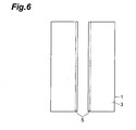
- Forming the starting point region for cutting 8 within the object 1 makes it easier to generate fractures from the starting point region for cutting 8 acting as a start point, whereby the object 1 can be cut with a relatively small force as illustrated in Fig. 6 . Therefore, the object 1 can be cut with a high precision without generating unnecessary fractures on the front face 3 of the object 1.
- the other is where the forming of the starting point region for cutting 8 causes the object 1 to fracture naturally in its cross-sectional direction (thickness direction) from the starting point region for cutting 8 acting as a start point, thereby cutting the object 1.
- the modified region formed by multiphoton absorption in the laser processing method in accordance with this embodiment encompasses the following cases (1) to (3):
- An object to be processed e.g., glass or a piezoelectric material made of LiTaO 3
- An object to be processed is irradiated with laser light while locating a converging point therewithin under a condition with a field intensity of at least 1 ⁇ 10 8 (W/cm 2 ) at the converging point and a pulse width of 1 ⁇ s or less.
- This magnitude of pulse width is a condition under which a crack region can be formed only within the object while generating multiphoton absorption without causing unnecessary damages to the front face of the object.
- This optical damage induces a thermal distortion within the object, thereby forming a crack region therewithin.
- the upper limit of field intensity is 1 ⁇ 10 12 (W/cm 2 ), for example.
- the pulse width is preferably 1 ns to 200 ns, for example.
- the inventors determined the relationship between field intensity and crack size by an experiment. The following are conditions of the experiment.
- the laser light quality of TEM 00 means that the converging characteristic is so high that convergence to about the wavelength of laser light is possible.
- Fig. 7 is a graph illustrating the results of the above-mentioned experiment.
- the abscissa indicates the peak power density. Since the laser light is pulsed laser light, the field intensity is represented by the peak power density.
- the ordinate indicates the size of a crack part (crack spot) formed within the object by one pulse of laser light. Crack spots gather to yield a crack region. The crack spot size is the size of a part yielding the maximum length among forms of crack spots.
- Data represented by black circles in the graph refer to a case where the converging lens (C) has a magnification of x100 and a numerical aperture (NA) of 0.80.
- data represented by whitened circles in the graph refer to a case where the converging lens (C) has a magnification of x50 and a numerical aperture (NA) of 0.55. Crack spots are seen to occur within the object from when the peak power density is about 10 11 (W/cm 2 ) and become greater as the peak power density increases.
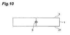
- FIG. 8 the object 1 is irradiated with laser light L while the converging point P is located within the object 1 under a condition where multiphoton absorption occurs, so as to form a crack region 9 therewithin along a line to cut.
- the crack region 9 is a region containing one or a plurality of cracks.
- a crack further grows from the crack region 9 acting as a start point (i.e., from the starting point region for cutting acting as a start point) as illustrated in Fig.
- An object to be processed e.g., semiconductor material such as silicon
- An object to be processed is irradiated with laser light while locating a converging point within the object under a condition with a field intensity of at least 1 ⁇ 10 8 (W/cm 2 ) at the converging point and a pulse width of 1 ⁇ s or less.
- the inside of the object is locally heated by multiphoton absorption. This heating forms a molten processed region within the object.
- the molten processed region encompasses regions once molten and then re-solidified, regions just in a molten state, and regions in the process of being re-solidified from the molten state, and can also be referred to as a region whose phase has changed or a region whose crystal structure has changed.
- the molten processed region may also be referred to as a region in which a certain structure has changed to another structure among monocrystal, amorphous, and polycrystal structures.
- the molten processed region is an amorphous silicon structure, for example.
- the upper limit of field intensity is 1 ⁇ 10 12 (W/cm 2 ), for example.
- the pulse width is preferably 1 ns to 200 ns, for example.
- the inventors verified that a molten processed region was formed within a silicon wafer (semiconductor substrate). The following are conditions of the experiment.
- Fig. 12 is a view illustrating a photograph of a cross section of a part of a silicon wafer cut by laser processing under the conditions mentioned above.
- a molten processed region 13 is formed within the silicon wafer 11.
- the molten processed region 13 formed under the above-mentioned conditions has a size of about 100 ⁇ m in the thickness direction.
- Fig. 13 is a graph illustrating relationships between the laser light wavelength and the transmittance within the silicon substrate.
- the respective reflected components on the front and rear sides of the silicon substrate are eliminated, so as to represent the internal transmittance alone.
- the respective relationships are illustrated in the cases where the thickness t of the silicon substrate is 50 ⁇ m, 100 ⁇ m, 200 ⁇ m, 500 ⁇ m, and 1000 ⁇ m.
- the laser light appears to be transmitted through the silicon substrate by at least 80% when the silicon substrate has a thickness of 500 ⁇ m or less.
- the silicon wafer 11 illustrated in Fig. 12 has a thickness of 350 ⁇ m, the molten processed region 13 caused by multiphoton absorption is formed near the center of the silicon wafer 11, i.e., at a part distanced from the front face by 175 ⁇ m.
- the transmittance in this case is 90% or more with reference to a silicon wafer having a thickness of 200 ⁇ m, whereby the laser light is absorbed only slightly within the silicon wafer 11 but is substantially transmitted therethrough.
- the molten processed region 13 is formed within the silicon wafer 11 not by the absorption of laser light within the silicon wafer 11 (i.e., not by usual heating with the laser light) but by multiphoton absorption.
- the forming of a molten processed region by multiphoton absorption is disclosed, for example, in " Ultrashort Pulse Laser Microprocessing of Silicon", Preprints of the National Meetings of Japan Welding Society, Vol. 66 (April, 2000), pp. 72-73 .
- a fracture is generated in a silicon wafer from a starting point region for cutting formed by a molten processed region, acting as a start point, in a cross-sectional direction, and reaches the front and rear faces of the silicon wafer, whereby the silicon wafer is cut.
- the fracture reaching the front and rear faces of the silicon wafer may grow naturally or as a force is applied to the silicon wafer.
- the fracture naturally growing from the starting point region for cutting to the front and rear faces of the silicon wafer encompasses a case where the fracture grows from a state in which the molten processed region forming the starting point region for cutting is molten and a case where the fracture grows when the molten processed region forming the starting point region for cutting is re-solidified from the molten state.
- the molten processed region is formed only within the silicon wafer, and thus is present only within the cut section after cutting as illustrated in Fig. 12 .
- a starting point region for cutting is thus formed within the object by a molten processed region, unnecessary fractures deviating from a starting point region for cutting line are harder to occur at the time of cleaving, whereby cleavage control becomes easier.
- the molten processed region may be formed not only by multiphoton absorption but also by other absorption actions.
- An object to be processed e.g., glass
- An object to be processed is irradiated with laser light while locating a converging point within the object under a condition with a field intensity of at least 1 ⁇ 10 8 (W/cm 2 ) at the converging point and a pulse width of 1 ns or less.
- a field intensity of at least 1 ⁇ 10 8 (W/cm 2 ) at the converging point and a pulse width of 1 ns or less.
- the upper limit of field intensity is 1 ⁇ 10 12 (W/cm 2 ), for example.
- the pulse width is preferably 1 ns or less, for example, more preferably 1 ps or less.
- the forming of a refractive index change region by multiphoton absorption is disclosed, for example, in " Forming of Photoinduced Structure within Glass by Femtosecond Laser Irradiation", Proceedings of the 42nd Laser Materials Processing Conference (November, 1997), pp. 105-111 .
- a starting point region for cutting may be formed as follows while taking account of the crystal structure of a wafer-like object to be processed, its cleavage characteristic, and the like, whereby the object can be cut with a favorable precision by a smaller force from the starting point region for cutting acting as a start point.
- a starting point region for cutting is formed in a direction extending along a (111) plane (first cleavage plane) or a (110) plane (second cleavage plane).
- a substrate made of a group III-V compound semiconductor of sphalerite structure such as GaAs
- a starting point region for cutting is formed in a direction extending along a (1120) plane (A plane) or a (1100) plane (M plane) while using a (0001) plane (C plane) as a principal plane.
- the substrate is formed with an orientation flat in a direction to be formed with the above-mentioned starting point region for cutting (e.g., a direction extending along a (111) plane in a monocrystal silicon substrate) or a direction orthogonal to the former direction
- the starting point region for cutting extending in the direction to be formed with the starting point region for cutting can be formed easily and accurately with reference to the orientation flat.
- an object to be processed 1 comprises a silicon wafer (semiconductor substrate) 11 having a thickness of 100 ⁇ m and a functional device layer 16 which is formed on a front face 11a of the silicon wafer 11 while including a plurality of functional devices 15.
- the object 1 is irradiated with processing laser light L1 while using the front face 3 as a laser light irradiation surface and locating a converging point P within the silicon wafer 11, so as to form a molten processed region 13 along each line to cut 5.
- the frame 22 and expandable tape 23 holding the object 1 are mounted to an expandable tape expander (not depicted), and the expandable tape 23 is expended outward, so as to cut the object 1 along the lines to cut 5 from the molten processed region 13 acting as a cutting start point and separate a number of semiconductor chips obtained by the cutting from each other.
- the foregoing can accurately cut the object 1 along the lines to cut 5.
- the molten processed region 13 may include cracks mixed therein.
- the laser processing apparatus 100 comprises a mount table 101 for mounting the object 1 horizontally, a laser unit 102, and a movement control section 103 connected to both of the mount table 101 and laser unit 102.
- the movement control section 103 moves the mount table 101 in horizontal directions (X and Y directions) and the laser unit 102 in vertical directions (Z directions).
- the laser unit 102 has a processing laser light source 104 for pulse-oscillating the processing laser light L1.
- the processing laser light L1 emitted from the processing laser light 104 successively passes through a shutter 105 for selectively transmitting and blocking the processing laser light L1 and a beam expander 106 for expanding the beam size, so as to be transmitted through a dichroic mirror 107, and then is converged by a converging lens 108, so as to irradiate the object 1.
- a piezoelectric device 109 for minutely adjusting the Z-directional position of the converging lens 108 is attached thereto.
- the laser unit 102 has a measuring laser light source 111 for emitting measuring laser light L2 for irradiating a processing region 30 which will be explained later.
- the measuring laser light L2 emitted from the measuring laser light source 111 is reflected by a mirror 112, a half mirror 113, and the dichroic mirror 107 in succession, so as to descend the optical axis of the processing laser light L1, and then is converged by the converging lens 108, so as to irradiate the processing region 30.
- the measuring laser light L2 having irradiated the processing region 30 is reflected by the processing region 30, and the resulting reflected light component L3 of the measuring laser light is made incident on the converging lens 108 again, so as to ascend the optical axis of the processing laser light L1, and then is reflected by the dichroic mirror 107, so as to be transmitted through the half mirror 113.
- the reflected light component L3 of the measuring laser light transmitted through the half mirror 113 is provided with astigmatism by a shaping optical system 114 composed of a cylindrical lens and a planoconvex lens and converged onto a light-receiving surface of a quadrant photodiode 115 formed by equally dividing a photodiode into four.
- a converged light image of the reflected light component L3 of the measuring laser light having the astigmatism added thereto is thus formed on the light-receiving surface of the quadrant photodiode 115, and consequently varies depending on the position of the converging point of the measuring laser light L3 with respect to the front face (laser sight irradiation surface) 3 of the object 1 positioned within the processing region 30.
- a converging lens control section 116 connected to the piezoelectric device 109 is connected to the quadrant photodiode 115.
- the converging lens control section 116 functions to detect the quantity of the reflected light component L3 of the measuring laser light reflected by the processing region 30, acquire the converged light image formed on the light-receiving surface of the quadrant photodiode 115 as a voltage value when the light quantity exceeds a predetermined threshold, drive the piezoelectric device 109 such that the voltage value becomes constant (i.e., the converged light image becomes constant), so as to keep a substantially constant distance between the front face 3 of the object 1 and the converging lens 108, and record the driving signal for the piezoelectric device 109 at that time.
- the rear face 21 of the object 1 is attached onto the expandable tape 23 stretched over the annular frame 22.
- the frame 22 and expandable tape 23 holding the object 1 are secured onto the mount table 101 of the laser processing apparatus 100.
- lines to cut 5 are set like grids passing between the functional devices 15, 15 adjacent to each other, and the processing region 30 having an outer diameter greater than the outer diameter of the object 1 but smaller than the inner diameter of the frame 22 is set with reference to at least one of the object 1 and frame 22.
- the processing region 30 has an outer shape between the object 1 and the frame 22.
- the mount table 101 is moved in a direction along which the lines to cut 5 parallel to the orientation flat 6 extend, so as to move the converging lens 108 relative to the object 1 in the direction of arrow B.
- the converging lens 108 is moved relative to the object 1 beyond the frame 22 because of the following reasons.
- an acceleration distance by which the relative moving speed becomes constant is required to be added to the relative movement distance of the converging lens 108 with respect to the object 1.
- the frame 22 for reliably cutting the object 1 along the lines to cut 5 from the modified region 13 acting as a cutting start point by expanding the expandable tape 23 outward, it is necessary for the frame 22 to be made as small as possible with respect to the object 1.
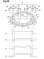
- the control signal for the measuring laser light source 111 changes from "OFF" to "ON” as illustrated in Fig. 20(a) , so that the measuring laser light L2 is emitted from the measuring laser light source 111 and converged by the converging lens 108.
- the measuring laser light L2 is reflected by the expandable tape 23 at this time, the quantity of the reflected light component L3 of the measuring laser light does not reach a threshold T as illustrated in Fig.
- the driving signal for the piezoelectric device 109 is "OFF" as illustrated in Fig. 20(c) , so that the converging lens 108 is held at a predetermined position.
- the converging lens 108 reaches one intersection ⁇ 1 between the outer edge of the object 1 and the line 50 including the line to cut 5
- the measuring laser light L2 is reflected by the front face 3 of the object 1, so that the quantity of the reflected light component L3 of the measuring laser light exceeds the threshold T as illustrated in Fig. 20(b) .
- the driving signal for the piezoelectric device 109 changes from "OFF" to "ON” as illustrated in Fig.
- the control signal for the shutter 105 changes from "OFF" to "ON” as illustrated in Fig. 20(d) , so that the processing laser light L1 emitted from the processing laser light source 104 is transmitted through the shutter 105 and converged by the converging lens 108. Consequently, the molten processed region 13 can accurately be formed at a constant distance (within the silicon wafer 11) from the front face 3 of the object 1 along the line to cut 5 even when the front face 3 of the object 1 wobbles.
- the timing at which the control signal for the shutter 105 changes from "OFF” to “ON” so as to irradiate the object 1 with the processing laser light L1 may be substantially the same as or slightly later than the timing at which the driving signal for the piezoelectric device 109 changes from "OFF" to "ON".
- the converging lens 108 reaches the other intersection ⁇ 2 between the outer edge of the object 1 and the line 50 including the line to cut 5
- the measuring laser light L2 is reflected by the expandable tape 23, so that the quantity of the reflected light component L3 of the measuring laser light falls from the threshold T as illustrated in Fig. 20(b) .
- the driving signal for the piezoelectric device 109 changes from "ON” to "OFF” as illustrated in Fig. 20(c) , whereby the converging lens 108 is held at the predetermined position.
- the control signal for the shutter 105 changes from "ON" to "OFF” as illustrated in Fig. 20(d) , so as to block the processing laser light L1 emitted from the processing laser light source 104.
- the control signal for the measuring laser light source 111 changes from "ON” to "OFF” as illustrated in Fig. 20(a) , so that the laser light source 111 stops emitting the measuring laser light L2.
- the laser processing method in accordance with this embodiment moves the converging lens 108 relative to the object 1 along the lines 50 including the lines to cut 5, converges the measuring laser light L2 toward the processing region 30 with the converging lens 108 when the converging lens 108 is positioned on the processing region 30 having the outer shape between the object 1 and frame 22, and detects the reflected light component L3 of the measuring laser light reflected by the front face 3 of the object 1.
- the processing laser light L1 is converged by the converging lens 108 toward the object 1, so as to form the molten processed region 13 within the object 1.
- the laser processing method in accordance with this embodiment converges the processing laser light L1 toward the object 1 with the converging lens 108, so as to form the molten processed region 13 within the object 1. This can prevent the frame 22 from being erroneously recognized as an object to be processed, so as to be irradiated with and damaged by the processing laser light L1, even when the converging lens 108 is moved relative to the object 1 beyond the frame 22.
- the present invention is not limited to the above-mentioned embodiment.
- the control in the laser processing apparatus 100 may be carried out as follows while performing the irradiation with the measuring laser light L2. Until the converging lens 108 reaches one intersection ⁇ 1 between the outer shape of the processing region 30 and the line 50 from one side, an arithmetic operation (hereinafter referred to as "autofocus arithmetic operation") based on the quantity of the reflected light component L3 of the measuring laser light for adjusting the distance between the front face 3 of the object 1 and the converging lens 108 is stopped, so as to secure the converging lens 108 at a constant position in the thickness direction of the object 1, and the irradiation with the processing laser light L1 is stopped.
- autofocus arithmetic operation based on the quantity of the reflected light component L3 of the measuring laser light for adjusting the distance between the front face 3 of the object 1 and the converging lens 108 is stopped, so as to secure the converging lens 108 at a constant position in the thickness direction of the object 1, and the irradi
- the converging lens 108 is secured at a constant position in the thickness direction of the object 1, and the irradiation with the processing laser light L1 is stopped.
- the converging lens 108 is secured at a predetermined position in the thickness direction of the object 1 even when carrying out the autofocus arithmetic operation, since the quantity of the reflected light component L3 of the measuring laser light does not exceed a predetermined threshold.
- the autofocus arithmetic operation is carried out, so as to adjust the distance between the front face 3 of the object 1 and the converging lens 108, and the irradiation with the processing laser light L1 is performed.
- the molten processed region 13 may be formed within the object 1 as follows after setting the processing region 30 having the outer shape between the object 1 and the frame 22.
- the converging lens 108 is moved relative to the object 1 along the line 50 including the line to cut 5, the measuring laser light L2 is converged toward the processing region 30 with the converging lens 108 when the converging lens 108 is positioned on the processing region 30, the reflected light component L3 of the measuring laser light reflected by the front face 3 of the object 1 is detected, so as to drive the piezoelectric device 109 such that the converging point P of the processing laser light L1 is positioned at a constant distance from the front face 3 of the object 1, thus keeping a substantially constant distance between the front face 3 of the object 1 and the converging lens 108, and the driving signal for the piezoelectric device 109 (adjustment information) at that time is recorded.
- the converging lens 108 is moved relative to the object 1 along the line 50 including the line to cut 5 and, while the recorded driving signal is reproduced so as to drive the piezoelectric device 109 when the converging lens 108 is positioned on the processing region 30, such that a substantially constant distance is kept between the front face 3 of the object 1 and the converging lens 108, the processing laser light L1 is converged toward the object 1 with the converging lens 108, so as to form the molten processed region 13 within the object 1.
- the timing at which the control signal for the shutter 105 changes from "OFF” to "ON", so as to irradiate the object 1 with the processing laser light L1, may be substantially the same as or slightly earlier than the timing at which the driving signal for the piezoelectric device 109 changes from "OFF" to "ON".
- the forming of the molten processed region 13 as in the foregoing is effective when the object 1 is relatively thick so that a plurality of rows of molten processed regions 13 are formed per line to cut such as to align in the thickness direction of the object 1.
- the distance between the front face 3 of the object 1 and the converging lens 108 is adjusted such that the converging point P of the processing laser light L1 is positioned at a constant distance from the front face 3 of the object 1 in the above-mentioned embodiment, but may be adjusted such that the converging point P of the processing laser light L1 is located at a predetermined position with reference to the front face 3 of the object 1.
- This can accurately form the modified region 13 at a predetermined position with reference to the front face 3 of the object 1, whereby a molten processed region 13 whose distance from the front face 3 of the object 1 changes therewithin, a wavy molten processed region 13, and the like can be formed along the lines to cut 5.
- the above-mentioned embodiment detects the reflected light component L3 of the measuring laser light reflected by the front face 3 of the object 1, the reflected light component L3 of the measuring laser light reflected by other laser light irradiation surfaces such as the rear face 21 of the object 1 may be detected.
- modified region 13 within the silicon wafer 11 of the object
- other modified regions such as crack regions and refractive index change regions may be formed within a wafer made of other materials such as glass and piezoelectric materials.
- the present invention can prevent the frame from being irradiated with and damaged by processing laser light.
Landscapes
- Physics & Mathematics (AREA)
- Optics & Photonics (AREA)
- Engineering & Computer Science (AREA)
- Mechanical Engineering (AREA)
- Plasma & Fusion (AREA)
- Chemical & Material Sciences (AREA)
- Chemical Kinetics & Catalysis (AREA)
- General Chemical & Material Sciences (AREA)
- Oil, Petroleum & Natural Gas (AREA)
- Laser Beam Processing (AREA)
- Dicing (AREA)
Applications Claiming Priority (2)
| Application Number | Priority Date | Filing Date | Title |
|---|---|---|---|
| JP2006273296 | 2006-10-04 | ||
| PCT/JP2007/068820 WO2008041604A1 (fr) | 2006-10-04 | 2007-09-27 | Procédé de traitement laser |
Publications (3)
| Publication Number | Publication Date |
|---|---|
| EP2070636A1 true EP2070636A1 (de) | 2009-06-17 |
| EP2070636A4 EP2070636A4 (de) | 2014-04-30 |
| EP2070636B1 EP2070636B1 (de) | 2015-08-05 |
Family
ID=39268465
Family Applications (1)
| Application Number | Title | Priority Date | Filing Date |
|---|---|---|---|
| EP07828566.5A Active EP2070636B1 (de) | 2006-10-04 | 2007-09-27 | Laserverarbeitungsverfahren |
Country Status (6)
| Country | Link |
|---|---|
| US (1) | US8735770B2 (de) |
| EP (1) | EP2070636B1 (de) |
| KR (1) | KR101428824B1 (de) |
| CN (3) | CN102357738B (de) |
| TW (1) | TWI432279B (de) |
| WO (1) | WO2008041604A1 (de) |
Families Citing this family (58)
| Publication number | Priority date | Publication date | Assignee | Title |
|---|---|---|---|---|
| JP4659300B2 (ja) * | 2000-09-13 | 2011-03-30 | 浜松ホトニクス株式会社 | レーザ加工方法及び半導体チップの製造方法 |
| CN101335235B (zh) * | 2002-03-12 | 2010-10-13 | 浜松光子学株式会社 | 基板的分割方法 |
| AU2003211581A1 (en) * | 2002-03-12 | 2003-09-22 | Hamamatsu Photonics K.K. | Method of cutting processed object |
| TWI326626B (en) * | 2002-03-12 | 2010-07-01 | Hamamatsu Photonics Kk | Laser processing method |
| TWI520269B (zh) | 2002-12-03 | 2016-02-01 | 濱松赫德尼古斯股份有限公司 | Cutting method of semiconductor substrate |
| FR2852250B1 (fr) * | 2003-03-11 | 2009-07-24 | Jean Luc Jouvin | Fourreau de protection pour canule, un ensemble d'injection comportant un tel fourreau et aiguille equipee d'un tel fourreau |
| DE60315515T2 (de) * | 2003-03-12 | 2007-12-13 | Hamamatsu Photonics K.K., Hamamatsu | Laserstrahlbearbeitungsverfahren |
| EP2269765B1 (de) * | 2003-07-18 | 2014-10-15 | Hamamatsu Photonics K.K. | Geschnittener Halbleiterchip |
| JP4563097B2 (ja) | 2003-09-10 | 2010-10-13 | 浜松ホトニクス株式会社 | 半導体基板の切断方法 |
| JP4601965B2 (ja) * | 2004-01-09 | 2010-12-22 | 浜松ホトニクス株式会社 | レーザ加工方法及びレーザ加工装置 |
| JP4598407B2 (ja) * | 2004-01-09 | 2010-12-15 | 浜松ホトニクス株式会社 | レーザ加工方法及びレーザ加工装置 |
| JP4509578B2 (ja) | 2004-01-09 | 2010-07-21 | 浜松ホトニクス株式会社 | レーザ加工方法及びレーザ加工装置 |
| EP1742253B1 (de) | 2004-03-30 | 2012-05-09 | Hamamatsu Photonics K.K. | Laserverarbeitungsverfahren |
| KR101190454B1 (ko) * | 2004-08-06 | 2012-10-11 | 하마마츠 포토닉스 가부시키가이샤 | 레이저 가공 장치 |
| JP4762653B2 (ja) * | 2005-09-16 | 2011-08-31 | 浜松ホトニクス株式会社 | レーザ加工方法及びレーザ加工装置 |
| JP4907965B2 (ja) * | 2005-11-25 | 2012-04-04 | 浜松ホトニクス株式会社 | レーザ加工方法 |
| JP4804911B2 (ja) * | 2005-12-22 | 2011-11-02 | 浜松ホトニクス株式会社 | レーザ加工装置 |
| JP4907984B2 (ja) * | 2005-12-27 | 2012-04-04 | 浜松ホトニクス株式会社 | レーザ加工方法及び半導体チップ |
| EP1875983B1 (de) | 2006-07-03 | 2013-09-11 | Hamamatsu Photonics K.K. | Laserbearbeitungsverfahren und hergestelltes Chip |
| JP5183892B2 (ja) | 2006-07-03 | 2013-04-17 | 浜松ホトニクス株式会社 | レーザ加工方法 |
| JP4954653B2 (ja) | 2006-09-19 | 2012-06-20 | 浜松ホトニクス株式会社 | レーザ加工方法 |
| EP2065120B1 (de) * | 2006-09-19 | 2015-07-01 | Hamamatsu Photonics K.K. | Laserbearbeitungsverfahren |
| JP5101073B2 (ja) * | 2006-10-02 | 2012-12-19 | 浜松ホトニクス株式会社 | レーザ加工装置 |
| JP4964554B2 (ja) * | 2006-10-03 | 2012-07-04 | 浜松ホトニクス株式会社 | レーザ加工方法 |
| JP5132911B2 (ja) * | 2006-10-03 | 2013-01-30 | 浜松ホトニクス株式会社 | レーザ加工方法 |
| JP5336054B2 (ja) * | 2007-07-18 | 2013-11-06 | 浜松ホトニクス株式会社 | 加工情報供給装置を備える加工情報供給システム |
| JP5449665B2 (ja) * | 2007-10-30 | 2014-03-19 | 浜松ホトニクス株式会社 | レーザ加工方法 |
| JP5134928B2 (ja) * | 2007-11-30 | 2013-01-30 | 浜松ホトニクス株式会社 | 加工対象物研削方法 |
| JP5054496B2 (ja) * | 2007-11-30 | 2012-10-24 | 浜松ホトニクス株式会社 | 加工対象物切断方法 |
| JP5692969B2 (ja) | 2008-09-01 | 2015-04-01 | 浜松ホトニクス株式会社 | 収差補正方法、この収差補正方法を用いたレーザ加工方法、この収差補正方法を用いたレーザ照射方法、収差補正装置、及び、収差補正プログラム |
| JP5254761B2 (ja) | 2008-11-28 | 2013-08-07 | 浜松ホトニクス株式会社 | レーザ加工装置 |
| JP5241527B2 (ja) | 2009-01-09 | 2013-07-17 | 浜松ホトニクス株式会社 | レーザ加工装置 |
| JP5241525B2 (ja) | 2009-01-09 | 2013-07-17 | 浜松ホトニクス株式会社 | レーザ加工装置 |
| JP5632751B2 (ja) | 2009-02-09 | 2014-11-26 | 浜松ホトニクス株式会社 | 加工対象物切断方法 |
| KR101769158B1 (ko) | 2009-04-07 | 2017-08-17 | 하마마츠 포토닉스 가부시키가이샤 | 레이저 가공 장치 및 레이저 가공 방법 |
| JP5491761B2 (ja) | 2009-04-20 | 2014-05-14 | 浜松ホトニクス株式会社 | レーザ加工装置 |
| DE102010009015A1 (de) * | 2010-02-24 | 2011-08-25 | OSRAM Opto Semiconductors GmbH, 93055 | Verfahren zum Herstellen einer Mehrzahl von optoelektronischen Halbleiterchips |
| DE112011100039B4 (de) * | 2010-06-14 | 2014-01-02 | Mitsubishi Electric Corp. | Laserbearbeitungsvorrichtung und Laserbearbeitungsverfahren |
| US8722516B2 (en) | 2010-09-28 | 2014-05-13 | Hamamatsu Photonics K.K. | Laser processing method and method for manufacturing light-emitting device |
| US8703517B2 (en) * | 2010-10-29 | 2014-04-22 | Denso Corporation | Method of Manufacturing a Semiconductor Device Including Removing a Reformed Layer |
| CN107490815B (zh) * | 2012-09-11 | 2020-03-17 | 新加坡恒立私人有限公司 | 截断型镜片、截断型镜片对及相应装置的制造 |
| JP5947741B2 (ja) * | 2013-03-29 | 2016-07-06 | トヨタ自動車株式会社 | 溶接部の検査装置とその検査方法 |
| DE102013104986A1 (de) * | 2013-05-15 | 2014-12-04 | Limo Patentverwaltung Gmbh & Co. Kg | Vorrichtung zur Beaufschlagung der Außenseite eines rotationssymmetrischen Bauteils mit Laserstrahlung |
| CN108178943B (zh) * | 2013-12-20 | 2020-04-21 | 日华化学株式会社 | 车辆座椅用阻燃性涂布剂及阻燃性车辆座椅材料的制造方法 |
| CN104889577A (zh) * | 2015-06-23 | 2015-09-09 | 无锡宏纳科技有限公司 | 一种平面光波导分路器晶圆激光切割工艺 |
| US12191168B2 (en) * | 2018-04-09 | 2025-01-07 | Tokyo Electron Limited | Laser processing device, laser processing system and laser processing method |
| JP7105639B2 (ja) | 2018-07-05 | 2022-07-25 | 浜松ホトニクス株式会社 | レーザ加工装置 |
| US10576585B1 (en) | 2018-12-29 | 2020-03-03 | Cree, Inc. | Laser-assisted method for parting crystalline material |
| US11024501B2 (en) | 2018-12-29 | 2021-06-01 | Cree, Inc. | Carrier-assisted method for parting crystalline material along laser damage region |
| US10562130B1 (en) | 2018-12-29 | 2020-02-18 | Cree, Inc. | Laser-assisted method for parting crystalline material |
| US10611052B1 (en) | 2019-05-17 | 2020-04-07 | Cree, Inc. | Silicon carbide wafers with relaxed positive bow and related methods |
| JP7270216B2 (ja) | 2019-08-23 | 2023-05-10 | パナソニックIpマネジメント株式会社 | レーザ加工装置、レーザ加工方法、および補正データ生成方法 |
| JP7343376B2 (ja) * | 2019-12-04 | 2023-09-12 | 株式会社ミツトヨ | レーザ加工装置 |
| JP7436219B2 (ja) * | 2020-01-27 | 2024-02-21 | 浜松ホトニクス株式会社 | レーザ加工装置、及び、レーザ加工方法 |
| JP7539066B2 (ja) | 2020-04-16 | 2024-08-23 | パナソニックIpマネジメント株式会社 | レーザ加工装置およびレーザ加工方法 |
| US12440925B2 (en) | 2020-07-15 | 2025-10-14 | Hamamatsu Photonics K.K. | Laser machining apparatus, laser machining method, and method for manufacturing semiconductor member |
| JP7629925B2 (ja) * | 2020-07-15 | 2025-02-14 | 浜松ホトニクス株式会社 | レーザ加工装置、及び、レーザ加工方法 |
| JP7487045B2 (ja) * | 2020-08-20 | 2024-05-20 | 浜松ホトニクス株式会社 | レーザ加工装置 |
Family Cites Families (65)
| Publication number | Priority date | Publication date | Assignee | Title |
|---|---|---|---|---|
| US4546231A (en) | 1983-11-14 | 1985-10-08 | Group Ii Manufacturing Ltd. | Creation of a parting zone in a crystal structure |
| KR0171947B1 (ko) | 1995-12-08 | 1999-03-20 | 김주용 | 반도체소자 제조를 위한 노광 방법 및 그를 이용한 노광장치 |
| US7392238B1 (en) * | 2000-08-23 | 2008-06-24 | Intel Corporation | Method and apparatus for concept-based searching across a network |
| JP4142694B2 (ja) | 2000-09-13 | 2008-09-03 | 浜松ホトニクス株式会社 | レーザ加工方法 |
| JP4659300B2 (ja) | 2000-09-13 | 2011-03-30 | 浜松ホトニクス株式会社 | レーザ加工方法及び半導体チップの製造方法 |
| JP3867102B2 (ja) * | 2000-09-13 | 2007-01-10 | 浜松ホトニクス株式会社 | 半導体材料基板の切断方法 |
| TWI326626B (en) | 2002-03-12 | 2010-07-01 | Hamamatsu Photonics Kk | Laser processing method |
| AU2003211581A1 (en) | 2002-03-12 | 2003-09-22 | Hamamatsu Photonics K.K. | Method of cutting processed object |
| JP4463796B2 (ja) | 2002-03-12 | 2010-05-19 | 浜松ホトニクス株式会社 | レーザ加工方法 |
| CN101335235B (zh) | 2002-03-12 | 2010-10-13 | 浜松光子学株式会社 | 基板的分割方法 |
| JP4693411B2 (ja) * | 2002-10-30 | 2011-06-01 | 株式会社半導体エネルギー研究所 | 半導体装置の作製方法 |
| TWI520269B (zh) | 2002-12-03 | 2016-02-01 | 濱松赫德尼古斯股份有限公司 | Cutting method of semiconductor substrate |
| ATE550129T1 (de) | 2002-12-05 | 2012-04-15 | Hamamatsu Photonics Kk | Laserbearbeitungsvorrichtungen |
| JP2004188422A (ja) * | 2002-12-06 | 2004-07-08 | Hamamatsu Photonics Kk | レーザ加工装置及びレーザ加工方法 |
| TWI248244B (en) * | 2003-02-19 | 2006-01-21 | J P Sercel Associates Inc | System and method for cutting using a variable astigmatic focal beam spot |
| FR2852250B1 (fr) | 2003-03-11 | 2009-07-24 | Jean Luc Jouvin | Fourreau de protection pour canule, un ensemble d'injection comportant un tel fourreau et aiguille equipee d'un tel fourreau |
| JP2004273895A (ja) | 2003-03-11 | 2004-09-30 | Disco Abrasive Syst Ltd | 半導体ウエーハの分割方法 |
| DE60315515T2 (de) | 2003-03-12 | 2007-12-13 | Hamamatsu Photonics K.K., Hamamatsu | Laserstrahlbearbeitungsverfahren |
| JP4640174B2 (ja) * | 2003-05-22 | 2011-03-02 | 株式会社東京精密 | レーザーダイシング装置 |
| EP2269765B1 (de) | 2003-07-18 | 2014-10-15 | Hamamatsu Photonics K.K. | Geschnittener Halbleiterchip |
| JP2005064230A (ja) * | 2003-08-12 | 2005-03-10 | Disco Abrasive Syst Ltd | 板状物の分割方法 |
| JP4563097B2 (ja) | 2003-09-10 | 2010-10-13 | 浜松ホトニクス株式会社 | 半導体基板の切断方法 |
| JP2005086175A (ja) | 2003-09-11 | 2005-03-31 | Hamamatsu Photonics Kk | 半導体薄膜の製造方法、半導体薄膜、半導体薄膜チップ、電子管、及び光検出素子 |
| TWI372462B (en) | 2003-10-28 | 2012-09-11 | Semiconductor Energy Lab | Method for manufacturing semiconductor device |
| EP1705764B1 (de) | 2004-01-07 | 2012-11-14 | Hamamatsu Photonics K. K. | Lichtemittierendes halbleiterbauelement und herstellungsverfahren dafür |
| JP4601965B2 (ja) | 2004-01-09 | 2010-12-22 | 浜松ホトニクス株式会社 | レーザ加工方法及びレーザ加工装置 |
| JP4598407B2 (ja) * | 2004-01-09 | 2010-12-15 | 浜松ホトニクス株式会社 | レーザ加工方法及びレーザ加工装置 |
| JP4509578B2 (ja) | 2004-01-09 | 2010-07-21 | 浜松ホトニクス株式会社 | レーザ加工方法及びレーザ加工装置 |
| CN1938827B (zh) | 2004-03-30 | 2010-05-26 | 浜松光子学株式会社 | 激光加工方法及半导体芯片 |
| JP4536407B2 (ja) | 2004-03-30 | 2010-09-01 | 浜松ホトニクス株式会社 | レーザ加工方法及び加工対象物 |
| EP1742253B1 (de) | 2004-03-30 | 2012-05-09 | Hamamatsu Photonics K.K. | Laserverarbeitungsverfahren |
| JP4439990B2 (ja) | 2004-04-28 | 2010-03-24 | 株式会社ディスコ | レーザー加工方法 |
| JP4582693B2 (ja) | 2004-06-29 | 2010-11-17 | 株式会社ディスコ | 切削装置 |
| JP4634089B2 (ja) | 2004-07-30 | 2011-02-16 | 浜松ホトニクス株式会社 | レーザ加工方法 |
| KR101190454B1 (ko) | 2004-08-06 | 2012-10-11 | 하마마츠 포토닉스 가부시키가이샤 | 레이저 가공 장치 |
| CN1295768C (zh) | 2004-08-09 | 2007-01-17 | 江苏长电科技股份有限公司 | 集成电路或分立元件超薄无脚封装工艺及其封装结构 |
| JP4440036B2 (ja) | 2004-08-11 | 2010-03-24 | 株式会社ディスコ | レーザー加工方法 |
| JP4754801B2 (ja) | 2004-10-13 | 2011-08-24 | 浜松ホトニクス株式会社 | レーザ加工方法 |
| JP4917257B2 (ja) | 2004-11-12 | 2012-04-18 | 浜松ホトニクス株式会社 | レーザ加工方法 |
| JP4781661B2 (ja) | 2004-11-12 | 2011-09-28 | 浜松ホトニクス株式会社 | レーザ加工方法 |
| JP4198123B2 (ja) | 2005-03-22 | 2008-12-17 | 浜松ホトニクス株式会社 | レーザ加工方法 |
| JP4630731B2 (ja) | 2005-05-30 | 2011-02-09 | 株式会社ディスコ | ウエーハの分割方法 |
| JP4776994B2 (ja) | 2005-07-04 | 2011-09-21 | 浜松ホトニクス株式会社 | 加工対象物切断方法 |
| JP4749799B2 (ja) | 2005-08-12 | 2011-08-17 | 浜松ホトニクス株式会社 | レーザ加工方法 |
| JP4762653B2 (ja) | 2005-09-16 | 2011-08-31 | 浜松ホトニクス株式会社 | レーザ加工方法及びレーザ加工装置 |
| JP4424302B2 (ja) | 2005-11-16 | 2010-03-03 | 株式会社デンソー | 半導体チップの製造方法 |
| JP4237745B2 (ja) | 2005-11-18 | 2009-03-11 | 浜松ホトニクス株式会社 | レーザ加工方法 |
| JP4907965B2 (ja) | 2005-11-25 | 2012-04-04 | 浜松ホトニクス株式会社 | レーザ加工方法 |
| JP4804911B2 (ja) | 2005-12-22 | 2011-11-02 | 浜松ホトニクス株式会社 | レーザ加工装置 |
| JP4907984B2 (ja) | 2005-12-27 | 2012-04-04 | 浜松ホトニクス株式会社 | レーザ加工方法及び半導体チップ |
| JP5183892B2 (ja) | 2006-07-03 | 2013-04-17 | 浜松ホトニクス株式会社 | レーザ加工方法 |
| EP1875983B1 (de) | 2006-07-03 | 2013-09-11 | Hamamatsu Photonics K.K. | Laserbearbeitungsverfahren und hergestelltes Chip |
| JP4954653B2 (ja) | 2006-09-19 | 2012-06-20 | 浜松ホトニクス株式会社 | レーザ加工方法 |
| EP2065120B1 (de) | 2006-09-19 | 2015-07-01 | Hamamatsu Photonics K.K. | Laserbearbeitungsverfahren |
| JP5101073B2 (ja) | 2006-10-02 | 2012-12-19 | 浜松ホトニクス株式会社 | レーザ加工装置 |
| JP5132911B2 (ja) | 2006-10-03 | 2013-01-30 | 浜松ホトニクス株式会社 | レーザ加工方法 |
| JP4964554B2 (ja) | 2006-10-03 | 2012-07-04 | 浜松ホトニクス株式会社 | レーザ加工方法 |
| JP5336054B2 (ja) | 2007-07-18 | 2013-11-06 | 浜松ホトニクス株式会社 | 加工情報供給装置を備える加工情報供給システム |
| JP4402708B2 (ja) | 2007-08-03 | 2010-01-20 | 浜松ホトニクス株式会社 | レーザ加工方法、レーザ加工装置及びその製造方法 |
| JP5225639B2 (ja) | 2007-09-06 | 2013-07-03 | 浜松ホトニクス株式会社 | 半導体レーザ素子の製造方法 |
| JP5342772B2 (ja) | 2007-10-12 | 2013-11-13 | 浜松ホトニクス株式会社 | 加工対象物切断方法 |
| JP5449665B2 (ja) | 2007-10-30 | 2014-03-19 | 浜松ホトニクス株式会社 | レーザ加工方法 |
| JP5134928B2 (ja) | 2007-11-30 | 2013-01-30 | 浜松ホトニクス株式会社 | 加工対象物研削方法 |
| JP5054496B2 (ja) | 2007-11-30 | 2012-10-24 | 浜松ホトニクス株式会社 | 加工対象物切断方法 |
| JP5241525B2 (ja) | 2009-01-09 | 2013-07-17 | 浜松ホトニクス株式会社 | レーザ加工装置 |
-
2007
- 2007-09-27 US US12/444,125 patent/US8735770B2/en active Active
- 2007-09-27 EP EP07828566.5A patent/EP2070636B1/de active Active
- 2007-09-27 CN CN201110319235.3A patent/CN102357738B/zh active Active
- 2007-09-27 KR KR1020097003670A patent/KR101428824B1/ko active Active
- 2007-09-27 CN CN201110319239.1A patent/CN102357739B/zh active Active
- 2007-09-27 WO PCT/JP2007/068820 patent/WO2008041604A1/ja not_active Ceased
- 2007-09-27 CN CN2007800372040A patent/CN101522362B/zh active Active
- 2007-10-01 TW TW096136776A patent/TWI432279B/zh active
Also Published As
| Publication number | Publication date |
|---|---|
| TW200902210A (en) | 2009-01-16 |
| US8735770B2 (en) | 2014-05-27 |
| EP2070636A4 (de) | 2014-04-30 |
| CN101522362B (zh) | 2012-11-14 |
| TWI432279B (zh) | 2014-04-01 |
| EP2070636B1 (de) | 2015-08-05 |
| CN102357738B (zh) | 2015-04-15 |
| CN102357738A (zh) | 2012-02-22 |
| WO2008041604A1 (fr) | 2008-04-10 |
| CN102357739A (zh) | 2012-02-22 |
| CN101522362A (zh) | 2009-09-02 |
| US20100032418A1 (en) | 2010-02-11 |
| CN102357739B (zh) | 2014-09-10 |
| KR20090073087A (ko) | 2009-07-02 |
| KR101428824B1 (ko) | 2014-08-11 |
Similar Documents
| Publication | Publication Date | Title |
|---|---|---|
| EP2070636B1 (de) | Laserverarbeitungsverfahren | |
| EP2070635B1 (de) | Laserbearbeitungsverfahren | |
| EP1959482B1 (de) | Laserbearbeitungsverfahren | |
| US8513567B2 (en) | Laser processing method for forming a modified region for cutting in an object | |
| US9012805B2 (en) | Laser working method | |
| EP2065120B1 (de) | Laserbearbeitungsverfahren | |
| US8278592B2 (en) | Laser processing method | |
| US8759948B2 (en) | Laser beam machining method and semiconductor chip | |
| EP2070634B1 (de) | Laserbearbeitungsvorrichtung | |
| US7592237B2 (en) | Laser processing method and object to be processed | |
| US8247734B2 (en) | Laser beam machining method | |
| US8946055B2 (en) | Laser processing method for cutting substrate and laminate part bonded to the substrate | |
| US8026154B2 (en) | Laser working method | |
| EP1906438B1 (de) | Verfahren zum schneiden eines werkstücks | |
| EP1867427B1 (de) | Laserbearbeitungsverfahren | |
| EP1609558B1 (de) | Laserstrahlbearbeitungsverfahren |
Legal Events
| Date | Code | Title | Description |
|---|---|---|---|
| PUAI | Public reference made under article 153(3) epc to a published international application that has entered the european phase |
Free format text: ORIGINAL CODE: 0009012 |
|
| 17P | Request for examination filed |
Effective date: 20090409 |
|
| AK | Designated contracting states |
Kind code of ref document: A1 Designated state(s): AT BE BG CH CY CZ DE DK EE ES FI FR GB GR HU IE IS IT LI LT LU LV MC MT NL PL PT RO SE SI SK TR |
|
| AX | Request for extension of the european patent |
Extension state: AL BA HR MK RS |
|
| DAX | Request for extension of the european patent (deleted) | ||
| A4 | Supplementary search report drawn up and despatched |
Effective date: 20140327 |
|
| RIC1 | Information provided on ipc code assigned before grant |
Ipc: B23K 26/06 20140101ALI20140321BHEP Ipc: H01L 21/02 20060101ALI20140321BHEP Ipc: H01L 21/78 20060101ALI20140321BHEP Ipc: B23K 26/38 20140101AFI20140321BHEP Ipc: B23K 26/40 20140101ALI20140321BHEP Ipc: B23K 26/00 20140101ALI20140321BHEP Ipc: H01L 21/301 20060101ALI20140321BHEP Ipc: B23K 26/04 20140101ALI20140321BHEP |
|
| GRAP | Despatch of communication of intention to grant a patent |
Free format text: ORIGINAL CODE: EPIDOSNIGR1 |
|
| INTG | Intention to grant announced |
Effective date: 20150212 |
|
| RIN1 | Information on inventor provided before grant (corrected) |
Inventor name: KUNO, KOJI Inventor name: SUZUKI, TATSUYA Inventor name: ATSUMI, KAZUHIRO |
|
| GRAS | Grant fee paid |
Free format text: ORIGINAL CODE: EPIDOSNIGR3 |
|
| GRAA | (expected) grant |
Free format text: ORIGINAL CODE: 0009210 |
|
| AK | Designated contracting states |
Kind code of ref document: B1 Designated state(s): AT BE BG CH CY CZ DE DK EE ES FI FR GB GR HU IE IS IT LI LT LU LV MC MT NL PL PT RO SE SI SK TR |
|
| REG | Reference to a national code |
Ref country code: GB Ref legal event code: FG4D |
|
| REG | Reference to a national code |
Ref country code: CH Ref legal event code: EP |
|
| REG | Reference to a national code |
Ref country code: AT Ref legal event code: REF Ref document number: 740411 Country of ref document: AT Kind code of ref document: T Effective date: 20150815 |
|
| REG | Reference to a national code |
Ref country code: IE Ref legal event code: FG4D |
|
| REG | Reference to a national code |
Ref country code: DE Ref legal event code: R096 Ref document number: 602007042467 Country of ref document: DE |
|
| REG | Reference to a national code |
Ref country code: AT Ref legal event code: MK05 Ref document number: 740411 Country of ref document: AT Kind code of ref document: T Effective date: 20150805 |
|
| REG | Reference to a national code |
Ref country code: LT Ref legal event code: MG4D |
|
| REG | Reference to a national code |
Ref country code: NL Ref legal event code: MP Effective date: 20150805 |
|
| PG25 | Lapsed in a contracting state [announced via postgrant information from national office to epo] |
Ref country code: LV Free format text: LAPSE BECAUSE OF FAILURE TO SUBMIT A TRANSLATION OF THE DESCRIPTION OR TO PAY THE FEE WITHIN THE PRESCRIBED TIME-LIMIT Effective date: 20150805 Ref country code: LT Free format text: LAPSE BECAUSE OF FAILURE TO SUBMIT A TRANSLATION OF THE DESCRIPTION OR TO PAY THE FEE WITHIN THE PRESCRIBED TIME-LIMIT Effective date: 20150805 Ref country code: GR Free format text: LAPSE BECAUSE OF FAILURE TO SUBMIT A TRANSLATION OF THE DESCRIPTION OR TO PAY THE FEE WITHIN THE PRESCRIBED TIME-LIMIT Effective date: 20151106 Ref country code: FI Free format text: LAPSE BECAUSE OF FAILURE TO SUBMIT A TRANSLATION OF THE DESCRIPTION OR TO PAY THE FEE WITHIN THE PRESCRIBED TIME-LIMIT Effective date: 20150805 |
|
| PG25 | Lapsed in a contracting state [announced via postgrant information from national office to epo] |
Ref country code: ES Free format text: LAPSE BECAUSE OF FAILURE TO SUBMIT A TRANSLATION OF THE DESCRIPTION OR TO PAY THE FEE WITHIN THE PRESCRIBED TIME-LIMIT Effective date: 20150805 Ref country code: IS Free format text: LAPSE BECAUSE OF FAILURE TO SUBMIT A TRANSLATION OF THE DESCRIPTION OR TO PAY THE FEE WITHIN THE PRESCRIBED TIME-LIMIT Effective date: 20151205 Ref country code: AT Free format text: LAPSE BECAUSE OF FAILURE TO SUBMIT A TRANSLATION OF THE DESCRIPTION OR TO PAY THE FEE WITHIN THE PRESCRIBED TIME-LIMIT Effective date: 20150805 Ref country code: PT Free format text: LAPSE BECAUSE OF FAILURE TO SUBMIT A TRANSLATION OF THE DESCRIPTION OR TO PAY THE FEE WITHIN THE PRESCRIBED TIME-LIMIT Effective date: 20151207 Ref country code: SE Free format text: LAPSE BECAUSE OF FAILURE TO SUBMIT A TRANSLATION OF THE DESCRIPTION OR TO PAY THE FEE WITHIN THE PRESCRIBED TIME-LIMIT Effective date: 20150805 Ref country code: PL Free format text: LAPSE BECAUSE OF FAILURE TO SUBMIT A TRANSLATION OF THE DESCRIPTION OR TO PAY THE FEE WITHIN THE PRESCRIBED TIME-LIMIT Effective date: 20150805 |
|
| PG25 | Lapsed in a contracting state [announced via postgrant information from national office to epo] |
Ref country code: NL Free format text: LAPSE BECAUSE OF FAILURE TO SUBMIT A TRANSLATION OF THE DESCRIPTION OR TO PAY THE FEE WITHIN THE PRESCRIBED TIME-LIMIT Effective date: 20150805 |
|
| PG25 | Lapsed in a contracting state [announced via postgrant information from national office to epo] |
Ref country code: EE Free format text: LAPSE BECAUSE OF FAILURE TO SUBMIT A TRANSLATION OF THE DESCRIPTION OR TO PAY THE FEE WITHIN THE PRESCRIBED TIME-LIMIT Effective date: 20150805 Ref country code: SK Free format text: LAPSE BECAUSE OF FAILURE TO SUBMIT A TRANSLATION OF THE DESCRIPTION OR TO PAY THE FEE WITHIN THE PRESCRIBED TIME-LIMIT Effective date: 20150805 Ref country code: DK Free format text: LAPSE BECAUSE OF FAILURE TO SUBMIT A TRANSLATION OF THE DESCRIPTION OR TO PAY THE FEE WITHIN THE PRESCRIBED TIME-LIMIT Effective date: 20150805 Ref country code: CZ Free format text: LAPSE BECAUSE OF FAILURE TO SUBMIT A TRANSLATION OF THE DESCRIPTION OR TO PAY THE FEE WITHIN THE PRESCRIBED TIME-LIMIT Effective date: 20150805 Ref country code: IT Free format text: LAPSE BECAUSE OF FAILURE TO SUBMIT A TRANSLATION OF THE DESCRIPTION OR TO PAY THE FEE WITHIN THE PRESCRIBED TIME-LIMIT Effective date: 20150805 |
|
| REG | Reference to a national code |
Ref country code: CH Ref legal event code: PL |
|
| REG | Reference to a national code |
Ref country code: DE Ref legal event code: R097 Ref document number: 602007042467 Country of ref document: DE |
|
| PG25 | Lapsed in a contracting state [announced via postgrant information from national office to epo] |
Ref country code: MC Free format text: LAPSE BECAUSE OF FAILURE TO SUBMIT A TRANSLATION OF THE DESCRIPTION OR TO PAY THE FEE WITHIN THE PRESCRIBED TIME-LIMIT Effective date: 20150805 Ref country code: RO Free format text: LAPSE BECAUSE OF FAILURE TO SUBMIT A TRANSLATION OF THE DESCRIPTION OR TO PAY THE FEE WITHIN THE PRESCRIBED TIME-LIMIT Effective date: 20150805 |
|
| PLBE | No opposition filed within time limit |
Free format text: ORIGINAL CODE: 0009261 |
|
| STAA | Information on the status of an ep patent application or granted ep patent |
Free format text: STATUS: NO OPPOSITION FILED WITHIN TIME LIMIT |
|
| REG | Reference to a national code |
Ref country code: IE Ref legal event code: MM4A |
|
| REG | Reference to a national code |
Ref country code: FR Ref legal event code: ST Effective date: 20160531 |
|
| 26N | No opposition filed |
Effective date: 20160509 |
|
| GBPC | Gb: european patent ceased through non-payment of renewal fee |
Effective date: 20151105 |
|
| PG25 | Lapsed in a contracting state [announced via postgrant information from national office to epo] |
Ref country code: LI Free format text: LAPSE BECAUSE OF NON-PAYMENT OF DUE FEES Effective date: 20150930 Ref country code: CH Free format text: LAPSE BECAUSE OF NON-PAYMENT OF DUE FEES Effective date: 20150930 Ref country code: IE Free format text: LAPSE BECAUSE OF NON-PAYMENT OF DUE FEES Effective date: 20150927 |
|
| PG25 | Lapsed in a contracting state [announced via postgrant information from national office to epo] |
Ref country code: SI Free format text: LAPSE BECAUSE OF FAILURE TO SUBMIT A TRANSLATION OF THE DESCRIPTION OR TO PAY THE FEE WITHIN THE PRESCRIBED TIME-LIMIT Effective date: 20150805 Ref country code: FR Free format text: LAPSE BECAUSE OF NON-PAYMENT OF DUE FEES Effective date: 20151005 |
|
| PG25 | Lapsed in a contracting state [announced via postgrant information from national office to epo] |
Ref country code: GB Free format text: LAPSE BECAUSE OF NON-PAYMENT OF DUE FEES Effective date: 20151105 |
|
| PG25 | Lapsed in a contracting state [announced via postgrant information from national office to epo] |
Ref country code: BE Free format text: LAPSE BECAUSE OF FAILURE TO SUBMIT A TRANSLATION OF THE DESCRIPTION OR TO PAY THE FEE WITHIN THE PRESCRIBED TIME-LIMIT Effective date: 20150805 |
|
| PG25 | Lapsed in a contracting state [announced via postgrant information from national office to epo] |
Ref country code: MT Free format text: LAPSE BECAUSE OF FAILURE TO SUBMIT A TRANSLATION OF THE DESCRIPTION OR TO PAY THE FEE WITHIN THE PRESCRIBED TIME-LIMIT Effective date: 20150805 |
|
| PG25 | Lapsed in a contracting state [announced via postgrant information from national office to epo] |
Ref country code: HU Free format text: LAPSE BECAUSE OF FAILURE TO SUBMIT A TRANSLATION OF THE DESCRIPTION OR TO PAY THE FEE WITHIN THE PRESCRIBED TIME-LIMIT; INVALID AB INITIO Effective date: 20070927 Ref country code: BG Free format text: LAPSE BECAUSE OF FAILURE TO SUBMIT A TRANSLATION OF THE DESCRIPTION OR TO PAY THE FEE WITHIN THE PRESCRIBED TIME-LIMIT Effective date: 20150805 |
|
| PG25 | Lapsed in a contracting state [announced via postgrant information from national office to epo] |
Ref country code: CY Free format text: LAPSE BECAUSE OF FAILURE TO SUBMIT A TRANSLATION OF THE DESCRIPTION OR TO PAY THE FEE WITHIN THE PRESCRIBED TIME-LIMIT Effective date: 20150805 |
|
| PG25 | Lapsed in a contracting state [announced via postgrant information from national office to epo] |
Ref country code: TR Free format text: LAPSE BECAUSE OF FAILURE TO SUBMIT A TRANSLATION OF THE DESCRIPTION OR TO PAY THE FEE WITHIN THE PRESCRIBED TIME-LIMIT Effective date: 20150805 |
|
| PG25 | Lapsed in a contracting state [announced via postgrant information from national office to epo] |
Ref country code: LU Free format text: LAPSE BECAUSE OF NON-PAYMENT OF DUE FEES Effective date: 20150927 |
|
| P01 | Opt-out of the competence of the unified patent court (upc) registered |
Effective date: 20230509 |
|
| PGFP | Annual fee paid to national office [announced via postgrant information from national office to epo] |
Ref country code: DE Payment date: 20250805 Year of fee payment: 19 |