EP2071293A2 - Capteur de position - Google Patents
Capteur de position Download PDFInfo
- Publication number
- EP2071293A2 EP2071293A2 EP08169943A EP08169943A EP2071293A2 EP 2071293 A2 EP2071293 A2 EP 2071293A2 EP 08169943 A EP08169943 A EP 08169943A EP 08169943 A EP08169943 A EP 08169943A EP 2071293 A2 EP2071293 A2 EP 2071293A2
- Authority
- EP
- European Patent Office
- Prior art keywords
- position sensor
- carrier
- spacer
- spacer element
- sensor according
- Prior art date
- Legal status (The legal status is an assumption and is not a legal conclusion. Google has not performed a legal analysis and makes no representation as to the accuracy of the status listed.)
- Granted
Links
- 125000006850 spacer group Chemical group 0.000 claims abstract description 105
- 238000005452 bending Methods 0.000 claims abstract description 7
- 229920000642 polymer Polymers 0.000 claims abstract description 5
- 238000007650 screen-printing Methods 0.000 claims abstract description 5
- 239000000969 carrier Substances 0.000 claims description 22
- 239000000463 material Substances 0.000 claims description 11
- 239000004020 conductor Substances 0.000 claims description 9
- 238000000034 method Methods 0.000 claims description 8
- 238000007639 printing Methods 0.000 claims description 6
- 239000012777 electrically insulating material Substances 0.000 claims description 3
- 238000003825 pressing Methods 0.000 claims description 3
- 230000001681 protective effect Effects 0.000 claims description 3
- 238000006073 displacement reaction Methods 0.000 claims description 2
- 238000004049 embossing Methods 0.000 claims description 2
- 229920001940 conductive polymer Polymers 0.000 description 2
- 230000001419 dependent effect Effects 0.000 description 2
- 239000011888 foil Substances 0.000 description 2
- 230000003993 interaction Effects 0.000 description 2
- 238000004519 manufacturing process Methods 0.000 description 2
- 239000004696 Poly ether ether ketone Substances 0.000 description 1
- 239000000853 adhesive Substances 0.000 description 1
- 230000001070 adhesive effect Effects 0.000 description 1
- JUPQTSLXMOCDHR-UHFFFAOYSA-N benzene-1,4-diol;bis(4-fluorophenyl)methanone Chemical compound OC1=CC=C(O)C=C1.C1=CC(F)=CC=C1C(=O)C1=CC=C(F)C=C1 JUPQTSLXMOCDHR-UHFFFAOYSA-N 0.000 description 1
- 238000010276 construction Methods 0.000 description 1
- 230000000694 effects Effects 0.000 description 1
- 238000011156 evaluation Methods 0.000 description 1
- 238000002955 isolation Methods 0.000 description 1
- 229920003223 poly(pyromellitimide-1,4-diphenyl ether) Polymers 0.000 description 1
- 229920000728 polyester Polymers 0.000 description 1
- 229920002530 polyetherether ketone Polymers 0.000 description 1
- 230000002035 prolonged effect Effects 0.000 description 1
- 229920001169 thermoplastic Polymers 0.000 description 1
- 229920001187 thermosetting polymer Polymers 0.000 description 1
- 239000004416 thermosoftening plastic Substances 0.000 description 1
- 238000009281 ultraviolet germicidal irradiation Methods 0.000 description 1
Images

Classifications
-
- G—PHYSICS
- G01—MEASURING; TESTING
- G01D—MEASURING NOT SPECIALLY ADAPTED FOR A SPECIFIC VARIABLE; ARRANGEMENTS FOR MEASURING TWO OR MORE VARIABLES NOT COVERED IN A SINGLE OTHER SUBCLASS; TARIFF METERING APPARATUS; MEASURING OR TESTING NOT OTHERWISE PROVIDED FOR
- G01D5/00—Mechanical means for transferring the output of a sensing member; Means for converting the output of a sensing member to another variable where the form or nature of the sensing member does not constrain the means for converting; Transducers not specially adapted for a specific variable
- G01D5/12—Mechanical means for transferring the output of a sensing member; Means for converting the output of a sensing member to another variable where the form or nature of the sensing member does not constrain the means for converting; Transducers not specially adapted for a specific variable using electric or magnetic means
- G01D5/14—Mechanical means for transferring the output of a sensing member; Means for converting the output of a sensing member to another variable where the form or nature of the sensing member does not constrain the means for converting; Transducers not specially adapted for a specific variable using electric or magnetic means influencing the magnitude of a current or voltage
- G01D5/16—Mechanical means for transferring the output of a sensing member; Means for converting the output of a sensing member to another variable where the form or nature of the sensing member does not constrain the means for converting; Transducers not specially adapted for a specific variable using electric or magnetic means influencing the magnitude of a current or voltage by varying resistance
- G01D5/165—Mechanical means for transferring the output of a sensing member; Means for converting the output of a sensing member to another variable where the form or nature of the sensing member does not constrain the means for converting; Transducers not specially adapted for a specific variable using electric or magnetic means influencing the magnitude of a current or voltage by varying resistance by relative movement of a point of contact or actuation and a resistive track
Definitions
- the present invention relates to a position sensor, in particular a potentiometer, having the features of the preamble of claim 1.
- a potentiometer position sensor in film construction known.
- This comprises a first carrier, which has at least one electrode of an electrical or electronic sensor circuit in a circuit region, and a second carrier, which is arranged opposite the first carrier and which has at least one other electrode of the sensor circuit.
- both carriers are designed as elastically bendable flexible film.
- such a position sensor comprises a spacer frame, by which the two carriers are fastened to each other, which laterally surrounds the circuit area and which distances the carriers from one another in an actuating direction, such that the electrodes of the sensor circuit are compressed by pressing and bending at least one of the carriers are contactable.
- the present invention addresses the problem of providing an improved embodiment for a position sensor of the type mentioned, which is characterized in particular by the fact that it has a relatively high reliability even at elevated ambient temperature.
- the invention is based on the general idea of providing at least one additional spacer in the form of a spacer element enclosed by the spacer frame on which the carriers can support one another at least when the sensor is actuated.
- the at least one spacer element with respect to positioning and / or dimensioning is chosen so that the operability of the sensor, so contacting its electrodes by bending at least one carrier is still possible.
- the second carrier designed as a foil receives support in the circuit area, at least when it is actuated. This results in the operation of the sensor in the second carrier to an increased voltage, since the second carrier must be bent more due to the at least one spacer element so that the electrodes can contact.
- the invention uses the knowledge that the film material of the second carrier at elevated operating temperature in the case of bending deformation can only generate reduced restoring forces, so that it is fundamentally possible that the electrode of the second carrier, in particular after a prolonged actuation at the same contact point remains at the at least one electrode of the first carrier at least for an impermissibly long time before it resets itself due to their elasticity. In this way, a conventional sensor may be at least temporarily at elevated ambient temperatures.
- the restoring forces within the second carrier are increased with the aid of the spacer elements proposed according to the invention, the latter can be significantly better removed from the first carrier when the actuation has ended.
- the reliability can be increased even at elevated ambient temperatures.
- the two carriers can always or at least during actuation of the position sensor over the at least one spacer element loosely abut each other. This means that the two carriers are not fastened to one another via the at least one spacer element, but are merely supported against one another via the at least one spacer element. This allows in particular relative movements between the respective carrier and the respective spacer element.
- the spacers can be realized in different ways.
- such a spacer can be formed by a polymer paste, which is printed on the respective carrier with a printing process, in particular with a screen printing process, and cured.
- a printing method is particularly advantageous if the particular electrode is formed on the respective carrier by an electrically conductive polymer paste and also in the printing process, in particular by screen printing, is printed on the respective carrier.
- the respective spacer element can also be formed by a film material that is glued to the respective carrier.
- sheet material is anyway used to produce at least the second carrier, so that such sheet material is available.
- the temperature expansion coefficients of the spacer element and of the respective carrier can be selected identically by using the same film materials, which increases the temperature resistance of the position sensor.
- the respective spacer element by embossing on the respective carrier.
- the respective carrier then also consists for example of a thermosetting plastic.
- the at least one spacer element may consist of an electrically insulating material, whereby interactions with the sensor circuit can be excluded.
- the respective spacer element consists of an electrically conductive material, wherein it can then simultaneously form part of the sensor circuit, such as e.g. a conductor for contacting one of the electrodes of the respective carrier and / or a protective resistor of the sensor circuit.
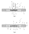
- a position sensor 1 comprises two carriers, namely a first carrier 2 and a second carrier 3. Furthermore, a spacer frame 4 is provided which fixes the two carriers 2, 3 to one another. At least the second carrier 3 is configured as an elastically bendable flexible film. In contrast, the first carrier 2 may in principle be made of a much stiffer material. However, an embodiment in which also the first carrier 2 is designed as an elastically bendable flexible film is preferred. Preference is given to the same sheet material as used in the second carrier 3. Also, the spacer frame 4 may be made of a corresponding foil material. The two carriers 2, 3 are expediently glued to the spacer frame 4.
- the first carrier 2 has at least one electrode 6 of an electrical or electronic sensor circuit 7 in a circuit region 5, which is symbolized here by a curly clamp.
- This sensor circuit 7 may in particular be a potentiometer circuit.
- a simple contact circuit for the realization of a switch is conceivable.
- the second carrier 3 also has at least one electrode 8 of this sensor circuit 7.
- the two carriers 2, 3 are positioned relative to each other by means of the spacer frame 4 so that they face each other and extend substantially parallel to each other. In the undeformed state, the carriers 2, 3 preferably each extend in a plane, wherein the two carriers 2, 3 are aligned relative to each other so that their planes extend parallel to each other.
- the spacer frame 4 encloses the circuit portion 5 laterally and is in its thickness direction, which is parallel to a in Fig. 1 extends indicated by an arrow operating direction 9, so dimensioned that the two carriers 2, 3 in the unactuated state according to Fig. 2 in this direction of actuation 9 a defined distance 10 from each other.
- Said distance 10 is chosen so that the electrodes 6, 8 of the two carriers 2, 3 can not touch in the unactuated state.
- Said distance 10 is thus greater than the thickness of the two electrodes 6, 8.
- the distance 10 between the carrier 2, 3 is further selected so that the electrodes 6, 8 by pressing the second carrier 3 against the first carrier 2, a contact of the opposite electrodes 6, 8 can be realized. According to Fig.
- the second carrier 3 bends so far that its at least one electrode 8 touches the at least one electrode 6 of the first carrier 2.
- the introduction of force to actuate the sensor 1 is realized here by means of an actuator 11, which for this purpose touches the second carrier 3 from the outside.
- an actuator 11 which for this purpose touches the second carrier 3 from the outside.
- embodiments with a non-contact operation are conceivable, for example by means of magnetic forces.
- At least one of the carriers 2, 3 is equipped with at least one spacer element 12 which is arranged in the circuit region 5, that is to say within the spacer frame 4. Furthermore, the respective spacer element 12 is located laterally next to the at least one electrode 6 or 8 of the respective carrier 2, 3 Fig. 1
- the two carriers 2, 3 can be supported against one another via the at least one spacer element 12, at least when the position sensor 1 is actuated, when the second carrier 3 is actuated accordingly.
- the second carrier 3 must be more deformed to the desired contact bring the electrodes 6, 8.
- 3 larger voltages are built up in the second carrier, which have increased restoring forces due to the elasticity of the bending deformation.
- a total of two spacer elements 12 are provided, which are arranged on both sides of the electrode 6 of the first carrier 2 on the first carrier 2.
- the respective spacer element 12 in the actuation direction 9 has a thickness 13 which is greater than the thickness of the contacting one upon actuation of the position sensor 1 electrodes 6, 8 together.
- the thickness 13 of the respective spacer element 12 is equal to the distance 10 between the carriers 2, 3, which is defined by the thickness 14 of the spacer frame 4.
- the spacer elements 12 are then the same thickness as the spacer frame 4.
- the thickness 13 of the spacer elements 12 may be selected to be greater than the thickness 14 of the spacer frame 4.
- the thickness 13 of the spacer elements 12 is selected to be smaller than the distance 10 or smaller than the thickness 14 of the spacer frame 4. It is crucial that upon actuation of the sensor 1, the two supports 2, 3 are supported by the respective spacer element 12, before the electrodes 6, 8 contact.
- the spacer elements 12 are configured such that the two carriers 2, 3 can be supported loosely on each other via the respective spacer element 12, that is to say that the carriers 2, 3 are not fastened to one another via the spacer elements 12.
- the two spacer elements 12 are attached exclusively to the first carrier 2. It is also possible to attach the spacer elements 12 exclusively on the second carrier 3. Likewise, an embodiment is conceivable in which at least one such spacer element 12 is arranged both on the first carrier 2 and on the second carrier 3. In this case, it is also possible to position the spacer elements 12 such that, at least when the sensor 1 is actuated, a spacer element 12 of the one carrier 2 is supported on a spacer element 12 of the other carrier 3.
- the senor 1 is preferably a film sensor, that is to say a film-type sensor 1, in which the two carriers 2, 3 and the spacer frame 3 are designed as films.
- a film is characterized by a comparatively small thickness compared to its length and width.
- the films have a maximum thickness of 0.2 mm.
- the entire sensor circuit 7 or at least components thereof can be provided to realize the entire sensor circuit 7 or at least components thereof with a printing process in which an electrically conductive polymer paste is printed on the respective carrier 2, 3.
- Sietikvon be used.
- the respective spacer element 12 is formed by a polymer paste.
- This can be conveniently printed with a suitable printing process on the respective carrier 2, 3 and cured.
- a screen printing method is also suitable for this purpose.
- an adhesive suitable for e.g. is curable by UV irradiation.
- the spacer elements 12 may also be formed by film material, which is then adhesively bonded to the respective carrier 2, 3 in a suitable manner.
- the respective carrier 2, 3 has an embossment, which then forms the respective spacer element 12.
- the respective carrier 2, 3 may be formed from a thermoplastic film.
- the respective carrier 2, 3 then consists of PEEK.
- the in the Fig. 1 and 2 recognizable spacer elements 12 are designed identically and in particular have the same thicknesses 13. In another embodiment may be provided in principle, at least two spacer elements 12 to be provided with different thicknesses 13.
- the spacer elements 12 are arranged in the embodiment shown here in the circuit portion 5 so that between the sensor circuit 7 and the spacer frame 4 only one spacer element 12 is arranged, ie in the orientation of the sensor circuit 7 to the spacer frame 4 direction. In another embodiment, it may be provided to arrange at least two spacer elements 12 laterally next to one another in this direction, that is to say between the sensor circuit 7 and the spacer frame 4. This makes it possible, in particular in conjunction with a stepped thickness 13 of the spacer elements 12, to influence the return behavior of the second carrier 3 in a targeted manner.
- the sensor circuit 7 may be configured as a potentiometer circuit. Accordingly, the sensor circuit 7 comprises, for example on the first carrier 2, a resistance path 15 and a collector path 16, which form both electrodes 6 of the first carrier 2.
- the resistance path 15 and the collector path 16 are connected via corresponding conductor tracks 17 with terminals 18, via which an evaluation circuit to the sensor 1 can be connected.
- the two spacers 12 extend at the in Fig. 3 shown embodiment in each case over the entire length of the resistance path 15 and the collector path 16, whereby over the entire length of the measuring range of the sensor 1, the increased restoring force in the second carrier 3 can be realized.
- the spacer elements 12 are preferably made of an electrically insulating material, whereby an interaction with circuit components 6, 8, 15, 16, 17 can be excluded.
- Fig. 4 shows Fig. 4 an embodiment in which at least one of the spacer elements 12, here the above Distance element 12 'shown consists of an electrically conductive material and here also forms part of the sensor circuit 7.
- this spacer element 12 ' is integrated into one of the strip conductors 17 and can in particular form a section of this strip conductor 17.
- this spacer element 12 ' can realize a protective resistor which is integrated into the conductor track 17.
- Fig. 4 shows in the lower half of further variants of the spacer element 12.
- left rectangular spacer elements 12 shown, while right circular spacers 12"'are shown. This illustrates that it is not necessary to provide a spacer element 12 that extends along the sensor circuit 7 in an interruption-free manner. Rather, the same effect can be realized by a plurality of point spacers 12 "and 12"'in the reason.
- the position sensor 1 is thus preferably a potentiometer.
- a linear potentiometer 1 is shown purely by way of example, ie a linear displacement sensor.
- rotary potentiometer 1 can be realized in the same way, so rotary encoder.
- the spacer frame 4 encloses the circuit portion 5 suitably on all sides, whereby the sensor circuit 7 can be enclosed hermetically.
Landscapes
- Physics & Mathematics (AREA)
- General Physics & Mathematics (AREA)
- Measurement Of Length, Angles, Or The Like Using Electric Or Magnetic Means (AREA)
- Push-Button Switches (AREA)
- Transmission And Conversion Of Sensor Element Output (AREA)
Applications Claiming Priority (1)
| Application Number | Priority Date | Filing Date | Title |
|---|---|---|---|
| DE200710059988 DE102007059988A1 (de) | 2007-12-11 | 2007-12-11 | Positionssensor |
Publications (3)
| Publication Number | Publication Date |
|---|---|
| EP2071293A2 true EP2071293A2 (fr) | 2009-06-17 |
| EP2071293A3 EP2071293A3 (fr) | 2013-03-13 |
| EP2071293B1 EP2071293B1 (fr) | 2014-03-12 |
Family
ID=40566205
Family Applications (1)
| Application Number | Title | Priority Date | Filing Date |
|---|---|---|---|
| EP20080169943 Ceased EP2071293B1 (fr) | 2007-12-11 | 2008-11-26 | Capteur de position |
Country Status (2)
| Country | Link |
|---|---|
| EP (1) | EP2071293B1 (fr) |
| DE (1) | DE102007059988A1 (fr) |
Families Citing this family (2)
| Publication number | Priority date | Publication date | Assignee | Title |
|---|---|---|---|---|
| DE102010020372B4 (de) | 2010-05-12 | 2020-07-09 | Metallux Ag | Positionssensor |
| DE102015009990A1 (de) * | 2015-07-31 | 2017-02-02 | MAQUET GmbH | Vorrichtung zur Positionserfassung beweglicher Operationstisch-Komponenten |
Citations (1)
| Publication number | Priority date | Publication date | Assignee | Title |
|---|---|---|---|---|
| DE4335004A1 (de) | 1993-10-14 | 1995-04-20 | Hoffmann & Krippner Gmbh | Sensor |
Family Cites Families (2)
| Publication number | Priority date | Publication date | Assignee | Title |
|---|---|---|---|---|
| DE3710286A1 (de) * | 1987-03-28 | 1988-10-06 | Preh Elektro Feinmechanik | Weg- bzw. positionsgeber |
| DE20013047U1 (de) * | 2000-07-28 | 2000-11-30 | Hoffmann & Krippner GmbH, 74722 Buchen | Sensor |
-
2007
- 2007-12-11 DE DE200710059988 patent/DE102007059988A1/de not_active Withdrawn
-
2008
- 2008-11-26 EP EP20080169943 patent/EP2071293B1/fr not_active Ceased
Patent Citations (1)
| Publication number | Priority date | Publication date | Assignee | Title |
|---|---|---|---|---|
| DE4335004A1 (de) | 1993-10-14 | 1995-04-20 | Hoffmann & Krippner Gmbh | Sensor |
Also Published As
| Publication number | Publication date |
|---|---|
| DE102007059988A1 (de) | 2009-06-18 |
| EP2071293B1 (fr) | 2014-03-12 |
| EP2071293A3 (fr) | 2013-03-13 |
Similar Documents
| Publication | Publication Date | Title |
|---|---|---|
| DE2623229C2 (de) | Membranschalter | |
| DE2559681C2 (de) | Betätigungsvorrichtung zum wahlweisen Schließen mehrerer elektrischer Stromkreise | |
| EP1559195A1 (fr) | Detecteur capacitif d'approche et/ou de contact et corps en plastique electriquement conducteur pour un detecteur de ce type | |
| DE2319042B2 (de) | Tastatur | |
| DE2541231A1 (de) | Schalteinrichtung und verfahren zu ihrer herstellung | |
| EP0857351B1 (fr) | Commutateur avec film conducteur comme contact fixe et raccordement aux contacts de connexion | |
| DE2515185A1 (de) | Elektrischer schnappschalter | |
| EP2071293B1 (fr) | Capteur de position | |
| DE2439697B2 (de) | Druckschalter | |
| EP2081197B1 (fr) | Dispositif de détermination de l'emplacement d'un point de compression | |
| EP2230486B1 (fr) | Capteur de position | |
| DE2036453C3 (de) | Membranschalter | |
| DE3033808A1 (de) | Tastschalter | |
| DE3214454C2 (de) | Elektrischer Schalter in Folienbauweise | |
| EP2071276B1 (fr) | Capteur | |
| DE112021003522T5 (de) | Benutzerschnittstelle mit innovativem widerstands-kraftsensor | |
| DE102009025458B4 (de) | Sensor | |
| EP0975058A2 (fr) | Dispositif de contact | |
| DE69407016T2 (de) | Klemmvorrichtung für elektrischen Anschluss | |
| WO1987005433A1 (fr) | Resistance electrique variable | |
| DE10157113A1 (de) | Elektronische Baugruppe | |
| DE102005047480B4 (de) | Verfahren zur Herstellung eines elektrischen Schalters für flexible Anwendungen, insbesondere eines Mikroschalters | |
| DE102008061273B4 (de) | Foliensensor | |
| DE102005054266B3 (de) | Schaltfeld | |
| DE102011122862B3 (de) | Laminat zur Herstellung eines Schalters, Schalter sowie Laminatbahn mit Laminatelementen aus einem solchen Laminat und Verfahren zur Herstellung eines solchen Laminats |
Legal Events
| Date | Code | Title | Description |
|---|---|---|---|
| PUAI | Public reference made under article 153(3) epc to a published international application that has entered the european phase |
Free format text: ORIGINAL CODE: 0009012 |
|
| AK | Designated contracting states |
Kind code of ref document: A2 Designated state(s): AT BE BG CH CY CZ DE DK EE ES FI FR GB GR HR HU IE IS IT LI LT LU LV MC MT NL NO PL PT RO SE SI SK TR |
|
| AX | Request for extension of the european patent |
Extension state: AL BA MK RS |
|
| PUAL | Search report despatched |
Free format text: ORIGINAL CODE: 0009013 |
|
| AK | Designated contracting states |
Kind code of ref document: A3 Designated state(s): AT BE BG CH CY CZ DE DK EE ES FI FR GB GR HR HU IE IS IT LI LT LU LV MC MT NL NO PL PT RO SE SI SK TR |
|
| AX | Request for extension of the european patent |
Extension state: AL BA MK RS |
|
| RIC1 | Information provided on ipc code assigned before grant |
Ipc: G01D 5/165 20060101AFI20130205BHEP |
|
| 17P | Request for examination filed |
Effective date: 20130607 |
|
| RBV | Designated contracting states (corrected) |
Designated state(s): AT BE BG CH CY CZ DE DK EE ES FI FR GB GR HR HU IE IS IT LI LT LU LV MC MT NL NO PL PT RO SE SI SK TR |
|
| GRAP | Despatch of communication of intention to grant a patent |
Free format text: ORIGINAL CODE: EPIDOSNIGR1 |
|
| AKX | Designation fees paid |
Designated state(s): DE FR |
|
| INTG | Intention to grant announced |
Effective date: 20131030 |
|
| GRAS | Grant fee paid |
Free format text: ORIGINAL CODE: EPIDOSNIGR3 |
|
| GRAA | (expected) grant |
Free format text: ORIGINAL CODE: 0009210 |
|
| AK | Designated contracting states |
Kind code of ref document: B1 Designated state(s): DE FR |
|
| REG | Reference to a national code |
Ref country code: DE Ref legal event code: R096 Ref document number: 502008011445 Country of ref document: DE Effective date: 20140424 |
|
| REG | Reference to a national code |
Ref country code: DE Ref legal event code: R097 Ref document number: 502008011445 Country of ref document: DE |
|
| PLBE | No opposition filed within time limit |
Free format text: ORIGINAL CODE: 0009261 |
|
| STAA | Information on the status of an ep patent application or granted ep patent |
Free format text: STATUS: NO OPPOSITION FILED WITHIN TIME LIMIT |
|
| 26N | No opposition filed |
Effective date: 20141215 |
|
| REG | Reference to a national code |
Ref country code: DE Ref legal event code: R097 Ref document number: 502008011445 Country of ref document: DE Effective date: 20141215 |
|
| REG | Reference to a national code |
Ref country code: FR Ref legal event code: PLFP Year of fee payment: 8 |
|
| REG | Reference to a national code |
Ref country code: FR Ref legal event code: PLFP Year of fee payment: 9 |
|
| REG | Reference to a national code |
Ref country code: FR Ref legal event code: PLFP Year of fee payment: 10 |
|
| PGFP | Annual fee paid to national office [announced via postgrant information from national office to epo] |
Ref country code: FR Payment date: 20171129 Year of fee payment: 10 |
|
| PGFP | Annual fee paid to national office [announced via postgrant information from national office to epo] |
Ref country code: DE Payment date: 20180131 Year of fee payment: 10 |
|
| REG | Reference to a national code |
Ref country code: DE Ref legal event code: R119 Ref document number: 502008011445 Country of ref document: DE |
|
| PG25 | Lapsed in a contracting state [announced via postgrant information from national office to epo] |
Ref country code: DE Free format text: LAPSE BECAUSE OF NON-PAYMENT OF DUE FEES Effective date: 20190601 Ref country code: FR Free format text: LAPSE BECAUSE OF NON-PAYMENT OF DUE FEES Effective date: 20181130 |