EP2071622A2 - Dispositif semi-conducteur et sa fabrication - Google Patents
Dispositif semi-conducteur et sa fabrication Download PDFInfo
- Publication number
- EP2071622A2 EP2071622A2 EP08171700A EP08171700A EP2071622A2 EP 2071622 A2 EP2071622 A2 EP 2071622A2 EP 08171700 A EP08171700 A EP 08171700A EP 08171700 A EP08171700 A EP 08171700A EP 2071622 A2 EP2071622 A2 EP 2071622A2
- Authority
- EP
- European Patent Office
- Prior art keywords
- metal plate
- metal plates
- hole
- package
- semiconductor device
- Prior art date
- Legal status (The legal status is an assumption and is not a legal conclusion. Google has not performed a legal analysis and makes no representation as to the accuracy of the status listed.)
- Withdrawn
Links
Images


Classifications
-
- H—ELECTRICITY
- H05—ELECTRIC TECHNIQUES NOT OTHERWISE PROVIDED FOR
- H05K—PRINTED CIRCUITS; CASINGS OR CONSTRUCTIONAL DETAILS OF ELECTRIC APPARATUS; MANUFACTURE OF ASSEMBLAGES OF ELECTRICAL COMPONENTS
- H05K3/00—Apparatus or processes for manufacturing printed circuits
- H05K3/30—Assembling printed circuits with electric components, e.g. with resistors
- H05K3/32—Assembling printed circuits with electric components, e.g. with resistors electrically connecting electric components or wires to printed circuits
- H05K3/34—Assembling printed circuits with electric components, e.g. with resistors electrically connecting electric components or wires to printed circuits by soldering
-
- H—ELECTRICITY
- H10—SEMICONDUCTOR DEVICES; ELECTRIC SOLID-STATE DEVICES NOT OTHERWISE PROVIDED FOR
- H10W—GENERIC PACKAGES, INTERCONNECTIONS, CONNECTORS OR OTHER CONSTRUCTIONAL DETAILS OF DEVICES COVERED BY CLASS H10
- H10W70/00—Package substrates; Interposers; Redistribution layers [RDL]
- H10W70/60—Insulating or insulated package substrates; Interposers; Redistribution layers
- H10W70/67—Insulating or insulated package substrates; Interposers; Redistribution layers characterised by their insulating layers or insulating parts
- H10W70/68—Shapes or dispositions thereof
- H10W70/6875—Shapes or dispositions thereof being on a metallic substrate, e.g. insulated metal substrates [IMS]
-
- H—ELECTRICITY
- H05—ELECTRIC TECHNIQUES NOT OTHERWISE PROVIDED FOR
- H05K—PRINTED CIRCUITS; CASINGS OR CONSTRUCTIONAL DETAILS OF ELECTRIC APPARATUS; MANUFACTURE OF ASSEMBLAGES OF ELECTRICAL COMPONENTS
- H05K3/00—Apparatus or processes for manufacturing printed circuits
- H05K3/40—Forming printed elements for providing electric connections to or between printed circuits
-
- H—ELECTRICITY
- H05—ELECTRIC TECHNIQUES NOT OTHERWISE PROVIDED FOR
- H05K—PRINTED CIRCUITS; CASINGS OR CONSTRUCTIONAL DETAILS OF ELECTRIC APPARATUS; MANUFACTURE OF ASSEMBLAGES OF ELECTRICAL COMPONENTS
- H05K3/00—Apparatus or processes for manufacturing printed circuits
- H05K3/46—Manufacturing multilayer circuits
- H05K3/4602—Manufacturing multilayer circuits characterized by a special circuit board as base or central core whereon additional circuit layers are built or additional circuit boards are laminated
- H05K3/4608—Manufacturing multilayer circuits characterized by a special circuit board as base or central core whereon additional circuit layers are built or additional circuit boards are laminated comprising an electrically conductive base or core
-
- H—ELECTRICITY
- H05—ELECTRIC TECHNIQUES NOT OTHERWISE PROVIDED FOR
- H05K—PRINTED CIRCUITS; CASINGS OR CONSTRUCTIONAL DETAILS OF ELECTRIC APPARATUS; MANUFACTURE OF ASSEMBLAGES OF ELECTRICAL COMPONENTS
- H05K3/00—Apparatus or processes for manufacturing printed circuits
- H05K3/46—Manufacturing multilayer circuits
- H05K3/4611—Manufacturing multilayer circuits by laminating two or more circuit boards
- H05K3/4641—Manufacturing multilayer circuits by laminating two or more circuit boards having integrally laminated metal sheets or special power cores
-
- H—ELECTRICITY
- H10—SEMICONDUCTOR DEVICES; ELECTRIC SOLID-STATE DEVICES NOT OTHERWISE PROVIDED FOR
- H10W—GENERIC PACKAGES, INTERCONNECTIONS, CONNECTORS OR OTHER CONSTRUCTIONAL DETAILS OF DEVICES COVERED BY CLASS H10
- H10W70/00—Package substrates; Interposers; Redistribution layers [RDL]
- H10W70/01—Manufacture or treatment
- H10W70/05—Manufacture or treatment of insulating or insulated package substrates, or of interposers, or of redistribution layers
-
- H—ELECTRICITY
- H10—SEMICONDUCTOR DEVICES; ELECTRIC SOLID-STATE DEVICES NOT OTHERWISE PROVIDED FOR
- H10W—GENERIC PACKAGES, INTERCONNECTIONS, CONNECTORS OR OTHER CONSTRUCTIONAL DETAILS OF DEVICES COVERED BY CLASS H10
- H10W70/00—Package substrates; Interposers; Redistribution layers [RDL]
- H10W70/60—Insulating or insulated package substrates; Interposers; Redistribution layers
- H10W70/67—Insulating or insulated package substrates; Interposers; Redistribution layers characterised by their insulating layers or insulating parts
- H10W70/68—Shapes or dispositions thereof
- H10W70/685—Shapes or dispositions thereof comprising multiple insulating layers
-
- H—ELECTRICITY
- H05—ELECTRIC TECHNIQUES NOT OTHERWISE PROVIDED FOR
- H05K—PRINTED CIRCUITS; CASINGS OR CONSTRUCTIONAL DETAILS OF ELECTRIC APPARATUS; MANUFACTURE OF ASSEMBLAGES OF ELECTRICAL COMPONENTS
- H05K2201/00—Indexing scheme relating to printed circuits covered by H05K1/00
- H05K2201/03—Conductive materials
- H05K2201/0332—Structure of the conductor
- H05K2201/0335—Layered conductors or foils
- H05K2201/0355—Metal foils
-
- H—ELECTRICITY
- H05—ELECTRIC TECHNIQUES NOT OTHERWISE PROVIDED FOR
- H05K—PRINTED CIRCUITS; CASINGS OR CONSTRUCTIONAL DETAILS OF ELECTRIC APPARATUS; MANUFACTURE OF ASSEMBLAGES OF ELECTRICAL COMPONENTS
- H05K2203/00—Indexing scheme relating to apparatus or processes for manufacturing printed circuits covered by H05K3/00
- H05K2203/03—Metal processing
- H05K2203/0369—Etching selective parts of a metal substrate through part of its thickness, e.g. using etch resist
-
- H—ELECTRICITY
- H05—ELECTRIC TECHNIQUES NOT OTHERWISE PROVIDED FOR
- H05K—PRINTED CIRCUITS; CASINGS OR CONSTRUCTIONAL DETAILS OF ELECTRIC APPARATUS; MANUFACTURE OF ASSEMBLAGES OF ELECTRICAL COMPONENTS
- H05K2203/00—Indexing scheme relating to apparatus or processes for manufacturing printed circuits covered by H05K3/00
- H05K2203/07—Treatments involving liquids, e.g. plating, rinsing
- H05K2203/0703—Plating
- H05K2203/0733—Method for plating stud vias, i.e. massive vias formed by plating the bottom of a hole without plating on the walls
-
- H—ELECTRICITY
- H05—ELECTRIC TECHNIQUES NOT OTHERWISE PROVIDED FOR
- H05K—PRINTED CIRCUITS; CASINGS OR CONSTRUCTIONAL DETAILS OF ELECTRIC APPARATUS; MANUFACTURE OF ASSEMBLAGES OF ELECTRICAL COMPONENTS
- H05K2203/00—Indexing scheme relating to apparatus or processes for manufacturing printed circuits covered by H05K3/00
- H05K2203/14—Related to the order of processing steps
- H05K2203/1476—Same or similar kind of process performed in phases, e.g. coarse patterning followed by fine patterning
-
- H—ELECTRICITY
- H05—ELECTRIC TECHNIQUES NOT OTHERWISE PROVIDED FOR
- H05K—PRINTED CIRCUITS; CASINGS OR CONSTRUCTIONAL DETAILS OF ELECTRIC APPARATUS; MANUFACTURE OF ASSEMBLAGES OF ELECTRICAL COMPONENTS
- H05K3/00—Apparatus or processes for manufacturing printed circuits
- H05K3/02—Apparatus or processes for manufacturing printed circuits in which the conductive material is applied to the surface of the insulating support and is thereafter removed from such areas of the surface which are not intended for current conducting or shielding
- H05K3/06—Apparatus or processes for manufacturing printed circuits in which the conductive material is applied to the surface of the insulating support and is thereafter removed from such areas of the surface which are not intended for current conducting or shielding the conductive material being removed chemically or electrolytically, e.g. by photo-etch process
-
- Y—GENERAL TAGGING OF NEW TECHNOLOGICAL DEVELOPMENTS; GENERAL TAGGING OF CROSS-SECTIONAL TECHNOLOGIES SPANNING OVER SEVERAL SECTIONS OF THE IPC; TECHNICAL SUBJECTS COVERED BY FORMER USPC CROSS-REFERENCE ART COLLECTIONS [XRACs] AND DIGESTS
- Y10—TECHNICAL SUBJECTS COVERED BY FORMER USPC
- Y10T—TECHNICAL SUBJECTS COVERED BY FORMER US CLASSIFICATION
- Y10T29/00—Metal working
- Y10T29/49—Method of mechanical manufacture
- Y10T29/49002—Electrical device making
- Y10T29/49117—Conductor or circuit manufacturing
- Y10T29/49124—On flat or curved insulated base, e.g., printed circuit, etc.
- Y10T29/49126—Assembling bases
-
- Y—GENERAL TAGGING OF NEW TECHNOLOGICAL DEVELOPMENTS; GENERAL TAGGING OF CROSS-SECTIONAL TECHNOLOGIES SPANNING OVER SEVERAL SECTIONS OF THE IPC; TECHNICAL SUBJECTS COVERED BY FORMER USPC CROSS-REFERENCE ART COLLECTIONS [XRACs] AND DIGESTS
- Y10—TECHNICAL SUBJECTS COVERED BY FORMER USPC
- Y10T—TECHNICAL SUBJECTS COVERED BY FORMER US CLASSIFICATION
- Y10T29/00—Metal working
- Y10T29/49—Method of mechanical manufacture
- Y10T29/49002—Electrical device making
- Y10T29/49117—Conductor or circuit manufacturing
- Y10T29/49124—On flat or curved insulated base, e.g., printed circuit, etc.
- Y10T29/49128—Assembling formed circuit to base
-
- Y—GENERAL TAGGING OF NEW TECHNOLOGICAL DEVELOPMENTS; GENERAL TAGGING OF CROSS-SECTIONAL TECHNOLOGIES SPANNING OVER SEVERAL SECTIONS OF THE IPC; TECHNICAL SUBJECTS COVERED BY FORMER USPC CROSS-REFERENCE ART COLLECTIONS [XRACs] AND DIGESTS
- Y10—TECHNICAL SUBJECTS COVERED BY FORMER USPC
- Y10T—TECHNICAL SUBJECTS COVERED BY FORMER US CLASSIFICATION
- Y10T29/00—Metal working
- Y10T29/49—Method of mechanical manufacture
- Y10T29/49002—Electrical device making
- Y10T29/49117—Conductor or circuit manufacturing
- Y10T29/49124—On flat or curved insulated base, e.g., printed circuit, etc.
- Y10T29/49147—Assembling terminal to base
-
- Y—GENERAL TAGGING OF NEW TECHNOLOGICAL DEVELOPMENTS; GENERAL TAGGING OF CROSS-SECTIONAL TECHNOLOGIES SPANNING OVER SEVERAL SECTIONS OF THE IPC; TECHNICAL SUBJECTS COVERED BY FORMER USPC CROSS-REFERENCE ART COLLECTIONS [XRACs] AND DIGESTS
- Y10—TECHNICAL SUBJECTS COVERED BY FORMER USPC
- Y10T—TECHNICAL SUBJECTS COVERED BY FORMER US CLASSIFICATION
- Y10T29/00—Metal working
- Y10T29/49—Method of mechanical manufacture
- Y10T29/49002—Electrical device making
- Y10T29/49117—Conductor or circuit manufacturing
- Y10T29/49124—On flat or curved insulated base, e.g., printed circuit, etc.
- Y10T29/49155—Manufacturing circuit on or in base
-
- Y—GENERAL TAGGING OF NEW TECHNOLOGICAL DEVELOPMENTS; GENERAL TAGGING OF CROSS-SECTIONAL TECHNOLOGIES SPANNING OVER SEVERAL SECTIONS OF THE IPC; TECHNICAL SUBJECTS COVERED BY FORMER USPC CROSS-REFERENCE ART COLLECTIONS [XRACs] AND DIGESTS
- Y10—TECHNICAL SUBJECTS COVERED BY FORMER USPC
- Y10T—TECHNICAL SUBJECTS COVERED BY FORMER US CLASSIFICATION
- Y10T29/00—Metal working
- Y10T29/49—Method of mechanical manufacture
- Y10T29/49002—Electrical device making
- Y10T29/49117—Conductor or circuit manufacturing
- Y10T29/49169—Assembling electrical component directly to terminal or elongated conductor
Definitions
- the present disclosure relates to a package for a semiconductor device and a method of manufacturing the package for a semiconductor device.
- a through hole is formed on a core substrate (a glass epoxy resin substrate), to both surfaces of which coppers are laminated, by means of a drill, electroless copper plating and electrolytic copper plating are carried out to the core substrate, an etching processing is carried out to form wiring patterns to be electrically connected by a through hole plating coating (a conducting portion) on the both surfaces of the core substrate, and furthermore, a multilayered wiring pattern is formed by a buildup method (Patent Document 1).
- Patent Document 1 Japanese Patent Unexamined Publication No. 11-68319
- the related-art package for a semiconductor device has the following problems. More specifically, it is necessary to form through holes one by one on a core substrate obtained by impregnating a glass fiber with an epoxy resin by using a drill. For this reason, there is a problem in that a long time is required for a processing and a cost is increased. In the case in which the hole is formed by means of the drill, moreover, a hole diameter and a pitch of the through hole cannot be reduced. Therefore, there is a problem in that a wiring density cannot be increased. In many cases, furthermore, a power layer and a ground layer are provided as inner layers. They are formed by an electrolytic plated film. For this reason, there is a problem in that it is hard to increase a thickness and a resistance value is increased.
- the package for a semiconductor device according to independent claim 1 and the method of manufacturing the package for a semiconductor device according to claim 6 are provided. Further advantages, features, aspects and details are evident from the dependent claims, the description and the drawings. Exemplary embodiments of the present invention provide a package for a semiconductor device in which a high density wiring can be carried out and a resistance value can be reduced, and a method of manufacturing the package for a semiconductor device
- An exemplary embodiment of the present invention provides a package for a semiconductor device, comprising:
- One of the two metal plates is a power layer and the other is a ground layer.
- the insulating layer is formed by electrodeposition.
- the first terminal portion and the second terminal portion on a side of one of the surfaces of the core substrate are formed to be external connecting terminals.
- a bump is formed on the external connecting terminal.
- an exemplary embodiment of the present invention provides a method of manufacturing a package for a semiconductor device comprising the steps of:
- the first through holes, the second through holes and the projections of the two metal plates are formed by carrying out an etching processing over the metal plates.
- the first through holes, the second through holes and the projections of the two metal plates are formed by carrying out a press processing over the metal plates.
- the projection is formed by carrying out a cut-up processing over the metal plate.
- the second terminal portion is formed by carrying out a grinding processing over a convex portion provided on the metal plate to remove the insulating layer.
- a package for a semiconductor device comprises a core substrate having two metal plates, each of which includes a first through hole, a second through hole , a projection, and an insulating layer formed on its surface.
- the metal plates are stacked in a manner that the projections of the mutual metal plates enter the second through hole of the metal plate on a partner side, and the first through holes of the metal plates form a through hole penetrating the core substrate.
- a tip end of each of the projections of the metal plates is exposed to a surface of the metal plate on the partner side to form a first terminal portion, and a second terminal portion is exposed from the insulating layer and formed on a surface of the metal plate on a side where the first terminal portion of the metal plate on the partner side is exposed.
- Embodiments are also directed to apparatuses for carrying out the disclosed methods and including apparatus parts for performing described method steps.
- embodiments are also directed to methods by which the described apparatus operates or by which the described apparatus is manufactured. It may include method steps for carrying out functions of the apparatus or manufacturing parts of the apparatus. The method steps may be performed by way of hardware components, firmware, software, a computer programmed by appropriate software, by any combination thereof or in any other manner.
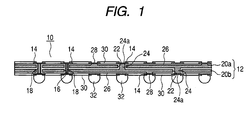
- Fig. 1 is a sectional view showing a package 10 for a semiconductor device according to the embodiment.
- the package 10 for a semiconductor device has a structure in which wiring patterns 14 are formed on a front surface and a back surface of a core substrate 12 and is connected electrically through a conducting portion 18 formed on a through hole 16 penetrating the core substrate 12.
- the core substrate 12 is formed by integrally providing the first through hole 16 for the conducting portion 18, a second through hole 22 and a projection 24 in each of two metal plates 20a and 20b, forming an insulating layer 26 on surfaces of each of the two metal plates 20a and 20b, and stacking the two metal plates 20a and 20b in such a manner that the projections 24 of the mutual metal plates 20a and 20b enter the second through hole 22 of the metal plate on a partner side. That is, the projection 24 of the metal plate 20a enters the second through hole 22 of the metal plate 20b, and the projection 24 of the metal plate 20b enters the second through hole 22 of the metal plate 20a.
- the insulating layer 26 is formed by carrying out an electrodeposition over a resin.
- the insulating layer 26 may be formed by another means such as coating in place of the electrodeposition. A thickness of the insulating layer 26 is not particularly restricted.
- the insulating layer 26 on a tip end of the projection 24 is removed and the tip end of the projection 24 is exposed to the surface of the metal plate on the partner side so that a first terminal portion 24a is formed, and a second terminal portion 28 exposed from the insulating layer 26 is formed in a predetermined portion on a surface of the metal plate on a side where the first terminal portion 24a of the metal plate on the partner side is exposed.
- the insulating layer 26 on a tip end of the projection 24 of the metal plate 20a is removed and the tip end of the projection 24 is exposed to the surface of the metal plate 20b so that a first terminal portion 24a is formed, and a second terminal portion 28 exposed from the insulating layer 26 is formed in a predetermined portion on a surface of the metal plate 20b on a side where the first terminal portion 24a of the metal plate 20a is exposed.
- the insulating layer 26 on a tip end of the projection 24 of the metal plate 20b is removed and the tip end of the projection 24 is exposed to the surface of the metal plate 20a so that a first terminal portion 24a is formed, and a second terminal portion 28 exposed from the insulating layer 26 is formed in a predetermined portion on a surface of the metal plate 20a on a side where the first terminal portion 24a of the metal plate 20b is exposed.
- Electroless copper plating and electrolytic copper plating are sequentially carried out over the conducting portion 18, the insulating layer 26, the first terminal portion 24a and the second terminal portion 28 to form a copper plated film.
- the copper plated film is subjected to an etching processing to form the wiring pattern 14.
- An insulating layer (a solder resist layer in the embodiment) 30 is formed on the wiring pattern 14, and a part of the insulating layer 30 is opened to expose the wiring pattern 14 so that a pad is formed.
- a wiring pattern itself for a first layer is formed as the pad in the embodiment, it is a matter of course that the wiring pattern may be formed to be multilayered by a buildup method.
- An external connecting bump 32 is formed on the pad at a lower surface side so that the package 10 for a semiconductor device is finished.
- a package for a semiconductor device of a PGA type by bonding a pin (not shown) in place of the bump 32.
- a pin (not shown)
- a package for a semiconductor device of an LGA type in which neither a bump nor a pin is attached.
- one of the two metal plates 20a and 20b is a power layer and the other as a ground layer.
- optional thicknesses can be selected.
- a metal plate having a thickness of approximately 200 ⁇ m for example, it is also possible to obtain a great strength and to decrease a resistance value, which is suitable.
- various hole forming processings can also be carried out easily with a small diameter and a small pitch through a press processing or an etching processing. Consequently, a high density wiring can be carried out.
- the hole diameters of the first through hole 16 and the second through hole 22 is approximately 50 ⁇ m to 700 ⁇ m and a pitch between the holes is approximately equal to or more than 100 ⁇ m.
- Materials of the metal plates 20a and 20b are not particularly restricted but a 42 alloy (an FeNi alloy) or a copper alloy material can be used.
- the diameter of the projection 24 is approximately 40 ⁇ m to 500 ⁇ m
- a pitch between the projections 24 is approximately equal to or more than 100 ⁇ m
- the thickness of the insulating layer 26 is approximately 5 ⁇ m to 100 ⁇ m.
- FIGs. 2A to 2J are views showing a process for forming the core substrate 12 through an etching processing and assembling the package 10 for a semiconductor device.
- one surface (front surface) of a metal plate 20 ( Fig. 2A ) is subjected to the etching processing to form a convex portion 34 ( Fig. 2B ).
- the etching processing is carried out by photolithography and a processing of forming and removing a resist pattern serving as a mask are required, description will be omitted (subsequent steps are the same).
- a hole 36 is formed by etching in portions to be a first through hole 16 and a second through hole 22 on the same one surface side of the metal plate 20 ( Fig. 2C ). Then, a back surface side is subjected to half etching to cause the hole 36 to penetrate, thereby forming the first through hole 16 and the second through hole 22 and forming a projection 24 ( Fig. 2D ).
- the projection 24 is formed by etching, it is possible to form the first through hole 16 and the second through hole 22 in the metal plate 20 in which the convex portion 34 is formed ( Figs. 6B and 6C ) and then form the projection 24 on the metal plate 20 (See Fig.
- a metal plate 20a is formed ( Fig. 2E ).
- the metal plate is subjected to the etching processing to form a metal plate 20b ( Fig. 2F ).
- the first through hole 16, the second through hole 22, the convex portion 34 and the projection 24 are also formed in the metal plate 20b.
- the insulating layer 26 is formed on the metal plate 20 through an electrodeposition and also formed in the first through hole 16, in the second through hole 22, on the convex portion 34 and on the projection 24.
- the two metal plates 20a and 20b are stacked in such a manner that the projections 24 of the mutual metal plates 20a and 20b enter the second through hole 22 of the metal plate on a partner side, and the core substrate 12 is thus formed.
- the two metal plates 20a and 20b may be specially bonded and integrated with an adhesive, it is also possible to bond the metal plates 20a and 20b through the insulating layer 26 and cure the insulating layer 26 to integrate the metal plates 20a and 20b by using a resin having an adhesiveness for the insulating layer 26.
- Fig. 3 is a plan view showing positions of the first through hole 16, the projection 24 and the convex portion 34 in a state in which the two metal plates 20a and 20b are stacked. It is a matter of course that an arrangement of the first through hole 16, the projection 24 and the convex portion 34 is not restricted thereto.
- electroless copper plating and electrolytic copper plating are sequentially carried out to form a conducting portion 18 in the first through hole 16, and a copper plated film is formed on a front surface and a back surface of the core substrate 12 and is subjected to etching to form a wiring pattern (pad) 14 ( Fig. 2I ).
- the wiring pattern 14 is covered to form an insulating layer (a solder resist layer) 30, and an exposure and a development are carried out to expose the pad 14.
- a bump 32 to be an external connecting terminal is formed on one of surface sides so that the package 10 for a semiconductor device can be finished.
- the wiring pattern 14 having one layer is formed on both sides of the core substrate, it is possible to properly form a wiring pattern having a plurality of layers by a buildup method.
- Fig. 4 is a partial explanatory view showing an embodiment in which two metal plates 20a and 20b are formed by a press processing and stacked, illustrating a state in which projections 24 of the mutual metal plates 20a and 20b enter second through holes 22 of the metal plates 20a and 20b on the partner side.
- a first through hole 16 (not shown) and a second through hole 22 can easily be formed on each of the metal plates 20a and 20b by means of a punch.
- a convex portion 34 is formed to be swollen toward an opposite side by pushing up the metal plate from a back side.
- the projection 24 is formed by cutting up the metal plate in an opposite direction to the convex portion 34.
- a hole generated by cutting up the metal plate may be buried with an insulating layer 26 covering the metal plate (not shown).
- a package 10 for a semiconductor device can be formed through the same steps as those in Figs. 2G to 2J . Also in the embodiment, an arrangement of the first through hole 16, the second through hole 22, the projection 24 and the convex portion 34 is optional.
- Fig. 5 is an explanatory view showing a further embodiment in which two metal plates 20a and 20b are formed by a press processing and stacked, illustrating a state in which projections 24 of the mutual metal plates 20a and 20b enter second through holes 22 of the metal plates 20a and 20b on a partner side.
- both of the projection 24 and a convex portion 34 are formed by a method of pushing up the metal plate from a back side.
- an insulating layer 26 is not shown.
- the metal plates 20a and 20b formed as described above are stacked to form a core substrate 12 as shown in Fig. 5 , and a package 10 for a semiconductor device can be formed through the same steps as those in Figs. 2G to 2J .
- an arrangement of a first through hole 16, a second through hole 22, the projection 24 and the convex portion 34 is optional.
Landscapes
- Engineering & Computer Science (AREA)
- Manufacturing & Machinery (AREA)
- Microelectronics & Electronic Packaging (AREA)
- Insulated Metal Substrates For Printed Circuits (AREA)
- Production Of Multi-Layered Print Wiring Board (AREA)
Applications Claiming Priority (1)
| Application Number | Priority Date | Filing Date | Title |
|---|---|---|---|
| JP2007322337A JP4825784B2 (ja) | 2007-12-13 | 2007-12-13 | 半導体装置用パッケージおよびその製造方法 |
Publications (2)
| Publication Number | Publication Date |
|---|---|
| EP2071622A2 true EP2071622A2 (fr) | 2009-06-17 |
| EP2071622A3 EP2071622A3 (fr) | 2011-09-07 |
Family
ID=40521741
Family Applications (1)
| Application Number | Title | Priority Date | Filing Date |
|---|---|---|---|
| EP08171700A Withdrawn EP2071622A3 (fr) | 2007-12-13 | 2008-12-15 | Dispositif semi-conducteur et sa fabrication |
Country Status (5)
| Country | Link |
|---|---|
| US (1) | US7963031B2 (fr) |
| EP (1) | EP2071622A3 (fr) |
| JP (1) | JP4825784B2 (fr) |
| KR (1) | KR20090063116A (fr) |
| TW (1) | TW200929478A (fr) |
Cited By (2)
| Publication number | Priority date | Publication date | Assignee | Title |
|---|---|---|---|---|
| EP2312920A2 (fr) * | 2009-10-02 | 2011-04-20 | Fujitsu Limited | Carte d'interconnexion, unité de carte de circuit imprimé et procédé |
| EP2587533A1 (fr) * | 2011-10-24 | 2013-05-01 | Shinko Electric Industries Co., Ltd. | Substrat de câblage, dispositif électroluminescent et procédé de fabrication du substrat de câblage |
Families Citing this family (3)
| Publication number | Priority date | Publication date | Assignee | Title |
|---|---|---|---|---|
| JP6017492B2 (ja) * | 2014-04-24 | 2016-11-02 | Towa株式会社 | 樹脂封止電子部品の製造方法、突起電極付き板状部材、及び樹脂封止電子部品 |
| JP5944445B2 (ja) | 2014-07-18 | 2016-07-05 | Towa株式会社 | 樹脂封止電子部品の製造方法、突起電極付き板状部材、樹脂封止電子部品、及び突起電極付き板状部材の製造方法 |
| JP7613104B2 (ja) * | 2021-01-04 | 2025-01-15 | 株式会社村田製作所 | インターポーザおよびこれを備える構造体 |
Citations (1)
| Publication number | Priority date | Publication date | Assignee | Title |
|---|---|---|---|---|
| JPH1168319A (ja) | 1997-08-11 | 1999-03-09 | Shinko Electric Ind Co Ltd | 多層回路基板及びその製造方法 |
Family Cites Families (16)
| Publication number | Priority date | Publication date | Assignee | Title |
|---|---|---|---|---|
| US4295183A (en) * | 1979-06-29 | 1981-10-13 | International Business Machines Corporation | Thin film metal package for LSI chips |
| JPS60109362A (ja) * | 1983-11-17 | 1985-06-14 | Fujitsu Ltd | 交換サ−ビス実行制御方式 |
| JP2000232283A (ja) * | 1999-02-10 | 2000-08-22 | Alps Electric Co Ltd | フレキシブルプリント基板の取付構造及びそれを用いた記録再生装置 |
| KR100333627B1 (ko) * | 2000-04-11 | 2002-04-22 | 구자홍 | 다층 인쇄회로기판 및 그 제조방법 |
| US6623651B2 (en) * | 2000-05-26 | 2003-09-23 | Visteon Global Technologies, Inc. | Circuit board and a method for making the same |
| JP4604403B2 (ja) * | 2001-06-25 | 2011-01-05 | パナソニック株式会社 | 固体電解コンデンサの製造方法 |
| US6713860B2 (en) * | 2002-02-01 | 2004-03-30 | Intel Corporation | Electronic assembly and system with vertically connected capacitors |
| JP2003289073A (ja) * | 2002-01-22 | 2003-10-10 | Canon Inc | 半導体装置および半導体装置の製造方法 |
| JP2003332752A (ja) * | 2002-05-14 | 2003-11-21 | Shinko Electric Ind Co Ltd | メタルコア基板およびその製造方法 |
| US6683781B2 (en) * | 2002-05-23 | 2004-01-27 | Industrial Technology Research Institute | Packaging structure with low switching noises |
| US6844505B1 (en) * | 2002-11-04 | 2005-01-18 | Ncr Corporation | Reducing noise effects in circuit boards |
| US20070211403A1 (en) * | 2003-12-05 | 2007-09-13 | Hrl Laboratories, Llc | Molded high impedance surface |
| US7548432B2 (en) * | 2005-03-24 | 2009-06-16 | Agency For Science, Technology And Research | Embedded capacitor structure |
| JP4553765B2 (ja) * | 2005-03-25 | 2010-09-29 | Okiセミコンダクタ株式会社 | 半導体装置の製造方法 |
| JP2007027683A (ja) * | 2005-06-15 | 2007-02-01 | Ngk Spark Plug Co Ltd | 配線基板及びその製造方法 |
| US20080171441A1 (en) * | 2005-06-28 | 2008-07-17 | Asahi Glass Co., Ltd. | Polishing compound and method for producing semiconductor integrated circuit device |
-
2007
- 2007-12-13 JP JP2007322337A patent/JP4825784B2/ja active Active
-
2008
- 2008-12-09 US US12/330,924 patent/US7963031B2/en active Active
- 2008-12-10 KR KR1020080125068A patent/KR20090063116A/ko not_active Withdrawn
- 2008-12-12 TW TW097148432A patent/TW200929478A/zh unknown
- 2008-12-15 EP EP08171700A patent/EP2071622A3/fr not_active Withdrawn
Patent Citations (1)
| Publication number | Priority date | Publication date | Assignee | Title |
|---|---|---|---|---|
| JPH1168319A (ja) | 1997-08-11 | 1999-03-09 | Shinko Electric Ind Co Ltd | 多層回路基板及びその製造方法 |
Cited By (3)
| Publication number | Priority date | Publication date | Assignee | Title |
|---|---|---|---|---|
| EP2312920A2 (fr) * | 2009-10-02 | 2011-04-20 | Fujitsu Limited | Carte d'interconnexion, unité de carte de circuit imprimé et procédé |
| EP2587533A1 (fr) * | 2011-10-24 | 2013-05-01 | Shinko Electric Industries Co., Ltd. | Substrat de câblage, dispositif électroluminescent et procédé de fabrication du substrat de câblage |
| US9257354B2 (en) | 2011-10-24 | 2016-02-09 | Shinko Electric Industries Co., Ltd. | Wiring substrate, light emitting device, and method for manufacturing wiring substrate |
Also Published As
| Publication number | Publication date |
|---|---|
| JP4825784B2 (ja) | 2011-11-30 |
| KR20090063116A (ko) | 2009-06-17 |
| JP2009147080A (ja) | 2009-07-02 |
| TW200929478A (en) | 2009-07-01 |
| US20090151995A1 (en) | 2009-06-18 |
| US7963031B2 (en) | 2011-06-21 |
| EP2071622A3 (fr) | 2011-09-07 |
Similar Documents
| Publication | Publication Date | Title |
|---|---|---|
| US7884484B2 (en) | Wiring board and method of manufacturing the same | |
| CN102612265B (zh) | 内置元件电路板、内置元件电路板的制造方法 | |
| TWI437647B (zh) | 具有凸塊/基座/凸緣層散熱座及增層電路之散熱增益型半導體組體 | |
| KR101344800B1 (ko) | 배선 기판 및 반도체 장치 | |
| KR101096614B1 (ko) | 전자 부품 실장 구조 및 그 제조 방법 | |
| KR100987688B1 (ko) | 프린트 배선 기판 및 프린트 배선 기판의 제조 방법 | |
| CN101515574B (zh) | 芯片封装载板、芯片封装体及其制造方法 | |
| CN102170745B (zh) | 多层布线板及其制造方法 | |
| JP3938921B2 (ja) | 半導体ic内蔵モジュールの製造方法 | |
| US9334576B2 (en) | Wiring substrate and method of manufacturing wiring substrate | |
| CN1202696C (zh) | 制作印刷电路板的方法 | |
| JP2009506572A (ja) | 相互接続構造を含むマイクロフィーチャ組立品およびそのような相互接続構造を形成するための方法 | |
| KR20070036007A (ko) | 반도체 ic 내장 기판 및 그 제조 방법 | |
| CN109788666B (zh) | 线路基板及其制作方法 | |
| CN105702649A (zh) | 具有整合双布线结构的线路板及其制作方法 | |
| JP2009252942A (ja) | 部品内蔵配線板、部品内蔵配線板の製造方法 | |
| US7963031B2 (en) | Package for semiconductor device and method of manufacturing the same | |
| CN1873935B (zh) | 配线基板的制造方法及半导体器件的制造方法 | |
| US7964106B2 (en) | Method for fabricating a packaging substrate | |
| US11923282B2 (en) | Wiring substrate | |
| JP2023061259A (ja) | 配線基板及びその製造方法 | |
| JP2005353837A (ja) | 半導体装置及びその製造方法 | |
| KR100894178B1 (ko) | 인쇄회로기판 제조방법 | |
| KR100919632B1 (ko) | 패키지 기판 및 그 제조방법 | |
| KR101158213B1 (ko) | 전자부품 내장형 인쇄회로기판 및 이의 제조 방법 |
Legal Events
| Date | Code | Title | Description |
|---|---|---|---|
| PUAI | Public reference made under article 153(3) epc to a published international application that has entered the european phase |
Free format text: ORIGINAL CODE: 0009012 |
|
| AK | Designated contracting states |
Kind code of ref document: A2 Designated state(s): AT BE BG CH CY CZ DE DK EE ES FI FR GB GR HR HU IE IS IT LI LT LU LV MC MT NL NO PL PT RO SE SI SK TR |
|
| AX | Request for extension of the european patent |
Extension state: AL BA MK RS |
|
| PUAL | Search report despatched |
Free format text: ORIGINAL CODE: 0009013 |
|
| AK | Designated contracting states |
Kind code of ref document: A3 Designated state(s): AT BE BG CH CY CZ DE DK EE ES FI FR GB GR HR HU IE IS IT LI LT LU LV MC MT NL NO PL PT RO SE SI SK TR |
|
| AX | Request for extension of the european patent |
Extension state: AL BA MK RS |
|
| RIC1 | Information provided on ipc code assigned before grant |
Ipc: H01L 23/14 20060101ALI20110729BHEP Ipc: H01L 21/48 20060101ALI20110729BHEP Ipc: H01L 23/498 20060101AFI20110729BHEP |
|
| STAA | Information on the status of an ep patent application or granted ep patent |
Free format text: STATUS: THE APPLICATION IS DEEMED TO BE WITHDRAWN |
|
| 18D | Application deemed to be withdrawn |
Effective date: 20110702 |