EP2071638A1 - Heterostructure electroluminescente semi-conductrice - Google Patents
Heterostructure electroluminescente semi-conductrice Download PDFInfo
- Publication number
- EP2071638A1 EP2071638A1 EP07834967A EP07834967A EP2071638A1 EP 2071638 A1 EP2071638 A1 EP 2071638A1 EP 07834967 A EP07834967 A EP 07834967A EP 07834967 A EP07834967 A EP 07834967A EP 2071638 A1 EP2071638 A1 EP 2071638A1
- Authority
- EP
- European Patent Office
- Prior art keywords
- type
- region
- layer
- nitride material
- gan
- Prior art date
- Legal status (The legal status is an assumption and is not a legal conclusion. Google has not performed a legal analysis and makes no representation as to the accuracy of the status listed.)
- Withdrawn
Links
Images
Classifications
-
- H—ELECTRICITY
- H10—SEMICONDUCTOR DEVICES; ELECTRIC SOLID-STATE DEVICES NOT OTHERWISE PROVIDED FOR
- H10H—INORGANIC LIGHT-EMITTING SEMICONDUCTOR DEVICES HAVING POTENTIAL BARRIERS
- H10H20/00—Individual inorganic light-emitting semiconductor devices having potential barriers, e.g. light-emitting diodes [LED]
- H10H20/80—Constructional details
- H10H20/81—Bodies
- H10H20/822—Materials of the light-emitting regions
- H10H20/824—Materials of the light-emitting regions comprising only Group III-V materials, e.g. GaP
- H10H20/825—Materials of the light-emitting regions comprising only Group III-V materials, e.g. GaP containing nitrogen, e.g. GaN
-
- H—ELECTRICITY
- H10—SEMICONDUCTOR DEVICES; ELECTRIC SOLID-STATE DEVICES NOT OTHERWISE PROVIDED FOR
- H10H—INORGANIC LIGHT-EMITTING SEMICONDUCTOR DEVICES HAVING POTENTIAL BARRIERS
- H10H20/00—Individual inorganic light-emitting semiconductor devices having potential barriers, e.g. light-emitting diodes [LED]
- H10H20/80—Constructional details
- H10H20/81—Bodies
- H10H20/811—Bodies having quantum effect structures or superlattices, e.g. tunnel junctions
- H10H20/812—Bodies having quantum effect structures or superlattices, e.g. tunnel junctions within the light-emitting regions, e.g. having quantum confinement structures
-
- H—ELECTRICITY
- H10—SEMICONDUCTOR DEVICES; ELECTRIC SOLID-STATE DEVICES NOT OTHERWISE PROVIDED FOR
- H10H—INORGANIC LIGHT-EMITTING SEMICONDUCTOR DEVICES HAVING POTENTIAL BARRIERS
- H10H20/00—Individual inorganic light-emitting semiconductor devices having potential barriers, e.g. light-emitting diodes [LED]
- H10H20/80—Constructional details
- H10H20/81—Bodies
- H10H20/811—Bodies having quantum effect structures or superlattices, e.g. tunnel junctions
-
- H—ELECTRICITY
- H10—SEMICONDUCTOR DEVICES; ELECTRIC SOLID-STATE DEVICES NOT OTHERWISE PROVIDED FOR
- H10H—INORGANIC LIGHT-EMITTING SEMICONDUCTOR DEVICES HAVING POTENTIAL BARRIERS
- H10H20/00—Individual inorganic light-emitting semiconductor devices having potential barriers, e.g. light-emitting diodes [LED]
- H10H20/80—Constructional details
- H10H20/81—Bodies
- H10H20/816—Bodies having carrier transport control structures, e.g. highly-doped semiconductor layers or current-blocking structures
Definitions
- an active area is formed in one of these areas, which contains at least one quantum well.
- the other area includes a current limiting layer.
- These include light-emitting semiconductor devices, in particular light-emitting diodes based on mixed crystals of the nitrides of the third metal group (solid solutions of nitrides of third group metals).
- Light-emitting heterostructures based on mixed crystals of the nitrides of the third metal group AllnGaN with pn junction are known. They contain a sequence of epitaxial layers. These epitaxial layers form an n-type and a p-type region (n- and p-type conductivity region). In the n-type region, the active area was formed, which has one or more quantum wells. In contrast, a broadband current limiting layer was arranged in the p-type region.
- the wide bandgap current-blocking layer is made of nitride material with a p-doped p-type alloy (see eg, US Pat. US 6515313 . RU 2262155 . RU 2277736 ).
- the holes from the p-type broadband current limiting layer are injected into the active region.
- the inversion of the electron injection into the p-region is an interfering process because the recombination in this region takes place without radiation.
- the p-type current limiting layer (barrier layer, emitter layer) is made of the p-type nitride material having a large width of the forbidden band. This current limiting layer prevents the electron penetration into the p-region. This contributes to increasing the hole injection efficiency effect and thus to increasing the external quantum efficiency of the luminous heterostructure.
- the characteristic feature of the considered halide heterostructures on the basis of mixed crystals of the nitrides of the third metal group AllnGaN is the presence of the integrated electric fields with a complicated configuration at the boundary GaN / AlGaN.
- the electrical limits arise as a result of the piezoelectric effect and the spontaneous polarization. It turns out that the ability of the current limiting layer to prevent electron penetration into the p-region is substantially suppressed.
- special measures have to be applied become. These measures serve to increase the energy barrier (potential barrier) for electrons in the current limiting layer and / or the increase in the hole concentration and the efficiency increase of the hole injection. This is achieved, inter alia, by the selection of the composition of the nitride compounds that form the current limiting layer.
- the closest prior art to the invention is a semiconductor light emitting heterostructure of the patent RU 2262155 ,
- the heterostructure in the direction of epitaxial growth consistently has an N-type contact layer and an active layer with a quantum well, and a broadband current-limiting layer and a P-type contact layer.
- the n-contact layer and the active layer are arranged in the n-type region.
- the quantum well is made of nitride material with the n-type alloy.
- the broadband current limiting layer (barrier layer) and the p-type contact layer are arranged in the p-type region.
- the broadband current limiting layer is made of nitride material AlGaN with the p-type alloy.
- the hole concentration at the active layer boundary is increased. This contributes to increasing the external quantum efficiency of the hole concentration.
- the recombination region is in the N region and the current confinement layer is in the P region.
- the heterostructures described above are characterized by the presence of strong integrated piezoelectric fields. However, the effect of hole injection into the active region is in increasing the pumping current in this heterostructure as well as in those described above Heterostructures back. Consequently, the external quantum efficiency of the heterostructure also decreases.
- the active region is located within the p-type region.
- the current limiting layer is in the n-type region.
- the semiconductor light-emitting structure in the direction of its epitaxial growth consequently comprises an n-type and a p-type region.
- the n-type region contains a successively arranged n-type nitride material layer (GaN) and a current limiting layer.
- the n-type nitride material layer (GaN) serves for current spreading.
- the current limiting layer is made of n-type nitride material (Al x Ga 1-x N).
- the p-type region includes a successively arranged p-type nitride (GaN) thin film, a quantum well active region, and a contact layer.
- the quantum wells are designed as layers of the non-alloyed nitride material (In y Ga 1-y N).
- the contact layer is made of p-type nitride material (GaN).
- the semiconductor light-emitting structure in the direction of its epitaxial growth includes a p-type region arranged in succession and an n-type region.
- the p-type region comprises a successively arranged p-type nitride material layer (GaN), an active region with quantum wells and a thin p-type nitride material layer (GaN).
- the active region is formed by layers of unalloyed nitride material (In y Ga 1-y N).
- the n-type region comprises a successively arranged current-limiting layer of n-type nitride material (Al x Ga 1 -x N) and a contact layer of n-type nitride material (GaN).
- the p-type nitride material layer (GaN) arranged in front of the active area has a region with a high p + degree of doping in its lower part.
- the heterostructure additionally includes a layer disposed in front of the high p + doping region and made of high n + dopant nitride material (GaN). This layer serves to propagate current and, together with the region with the high p + doping level, forms the reverse-biased pn tunnel junction.
- the fundamental distinguishing feature of the registered (inverse) to already known semiconductor light-emitting heterostructures is that the active area is placed in the p-area. This ensures that the intensity of the carrier recombination in the active area is not determined by the hole injection but by the electron injection.
- the broadband current limiting layer prevents the penetration of holes into the n-region.
- the inventors' computational and experimental research has shown that the barrier potential height created by the current confinement layer for the holes in such an inverse heterostructure based on mixed crystals of the nitrides of the third metal group AllnGaN will be large enough, even if the integrated electric fields to be taken into account. The proportion of holes that penetrate into the n-region and thus reduce the effectiveness of the electron injection is insignificant.
- the technical result of the filed invention is the creation of an energy barrier for the holes.
- this contributes to the increase of the carrier concentration in the active area. Accordingly, the external quantum efficiency of the applied heterostructure is increased. Their dependence on the pump current at high current density does not diminish.
- the design with a pn junction is possible for the registered semiconductor luminaire heterostructure. Consequently, this semiconductor light-emitting structure, in the direction of its epitaxial growth, first contains an n-type region and then a p-type region. Accordingly, the heterostructure in the n-type region includes an n-type nitride (GaN) layer for current spreading and an n-type nitride material (Al x Ga 1-x N) current confinement layer. Consequently, in the p-type region, the heterostructure contains a thin p-type nitride material (GaN) layer, a quantum well active region, and a contact layer. The quantum wells are formed by layers of unalloyed nitride material (In y Ga 1-y N). The contact layer is made of p-type nitride material (GaN).
- This heterostructure includes the active area with some quantum wells. Therefore, most of the radiation recombination of the electrons injected from the n-type region into the p-type region and the holes in this heterostructure are attributable to the lower well (the first well in the direction of epitaxial growth of the heterostructure).
- the lower trough in a Dahlmuldeneptept which the worst process material quality.
- the upper trough has the best material properties.
- Such a heterostructure contains in the direction of its epitaxial growth p- and n-type regions that form a pn junction.
- the p-type region sequentially includes the p-type nitride material layer (GaN), the quantum well active region, and the p-type nitride thin film (GaN).
- the quantum wells are formed by layers of unalloyed nitride material (In y Ga 1-y N).
- the n-type region sequentially includes the arranged current-limiting layer of n-type nitride material (Al x Ga 1-x N) and one Contact layer of n-type nitride material (GaN).
- a p-type nitride material layer (GaN) is arranged in front of the active area. In its lower part, this layer contains a region with a high p + degree of doping.
- the heterostructure also contains a layer which is provided for the current propagation and is made of nitride material (GaN) with a high n + degree of doping. This layer lies in front of the area with the high p + doping level and forms with this area a reverse-biased pn tunnel junction.
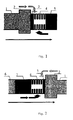
- layers 1 and 2 form an n-type region and layer 3, region 4 and layer 5 form a p-type region.
- Fig. 1 and 2 characterize the electron injection into the active area.
- the lower arrows show the hole injection into the active area.
- the arrow under Fig. 1 and Fig. 2 denotes the direction of epitaxial growth of the heterostructure.
- the applied heterostructure whose individual embodiments are described in Fig. 1 and 2 can be produced by the method of gas phase epitaxy of organometallic compounds on an insulating pad.
- the insulation pad can be made of sapphire, among others.
- the carrier recombination takes place in the quantum wells of the active region 4.
- the material width of these quantum wells is identical to the width of the forbidden energy band and is smaller than the width of the usual material of the active region 4.
- Fig. 2 the heterostructure is shown with two pn junctions.
- the radiation recombination takes place in the active area 4 of the upper pn junction.
- the main part of the carrier recombination in the upper trough comes about.
- the upper trough usually has the best process material quality.
- said heterostructure has the best light emission characteristics. It should be noted that (due to the bias of the lower pn transition in the reverse direction in the operating state of the heterostructure), this pn junction must be tunnel-transparent. Because of this he is through the Reason it is formed by the highly doped n + and p + regions, which are arranged in the lower part of the heterostructure in each of the layers 6 and 7.
- the registered semiconductor light-emitting structures can be used as light-emitting elements in household and industrial appliances and find application in various fields.
- the proposed semiconductor light-emitting heterostructures were tested in the Laboratory of Semiconductor and Quantum Physics of the Department of Physics and Technology (Fizikotexnicheskijinstitut in A.F.loffe) of the Russian Academy of Sciences and showed a relatively high external quantum efficiency. The experiments showed an unchanged external quantum efficiency with increasing pumping current.
Landscapes
- Led Devices (AREA)
Applications Claiming Priority (2)
| Application Number | Priority Date | Filing Date | Title |
|---|---|---|---|
| RU2006129223/28A RU2306634C1 (ru) | 2006-08-08 | 2006-08-08 | Полупроводниковая светоизлучающая гетероструктура |
| PCT/RU2007/000441 WO2008018817A1 (fr) | 2006-08-08 | 2007-08-01 | Hétérostructure électroluminescente semi-conductrice |
Publications (2)
| Publication Number | Publication Date |
|---|---|
| EP2071638A1 true EP2071638A1 (fr) | 2009-06-17 |
| EP2071638A4 EP2071638A4 (fr) | 2014-07-16 |
Family
ID=38695423
Family Applications (1)
| Application Number | Title | Priority Date | Filing Date |
|---|---|---|---|
| EP07834967.7A Withdrawn EP2071638A4 (fr) | 2006-08-08 | 2007-08-01 | Heterostructure electroluminescente semi-conductrice |
Country Status (3)
| Country | Link |
|---|---|
| EP (1) | EP2071638A4 (fr) |
| RU (1) | RU2306634C1 (fr) |
| WO (1) | WO2008018817A1 (fr) |
Families Citing this family (3)
| Publication number | Priority date | Publication date | Assignee | Title |
|---|---|---|---|---|
| RU2370857C1 (ru) * | 2008-06-05 | 2009-10-20 | Закрытое акционерное общество "ЭПИ-ЦЕНТР" | Полупроводниковая светоизлучающая гетероструктура |
| RU2381596C1 (ru) * | 2008-07-15 | 2010-02-10 | Закрытое акционерное общество "ЭПИ-ЦЕНТР" | Светодиодная гетероструктура |
| RU2400866C1 (ru) * | 2009-05-22 | 2010-09-27 | Государственное образовательное учреждение высшего профессионального образования "Нижегородский государственный университет им. Н.И. Лобачевского" | Светоизлучающий диод |
Family Cites Families (11)
| Publication number | Priority date | Publication date | Assignee | Title |
|---|---|---|---|---|
| EP0772249B1 (fr) * | 1995-11-06 | 2006-05-03 | Nichia Corporation | Dispositif semi-conducteur comprenant un composé de nitrure |
| SG63757A1 (en) * | 1997-03-12 | 1999-03-30 | Hewlett Packard Co | Adding impurities to improve the efficiency of allngan quantum well led's |
| US6515313B1 (en) | 1999-12-02 | 2003-02-04 | Cree Lighting Company | High efficiency light emitters with reduced polarization-induced charges |
| CN100521260C (zh) * | 2002-07-16 | 2009-07-29 | 氮化物半导体株式会社 | 氮化镓类化合物半导体装置 |
| US6835957B2 (en) * | 2002-07-30 | 2004-12-28 | Lumileds Lighting U.S., Llc | III-nitride light emitting device with p-type active layer |
| US6822991B2 (en) * | 2002-09-30 | 2004-11-23 | Lumileds Lighting U.S., Llc | Light emitting devices including tunnel junctions |
| RU2231171C1 (ru) * | 2003-04-30 | 2004-06-20 | Закрытое акционерное общество "Инновационная фирма "ТЕТИС" | Светоизлучающий диод |
| TWI233225B (en) * | 2004-09-03 | 2005-05-21 | Formosa Epitaxy Inc | GaN light emitting diode structure with high reverse withstanding voltage and high anti-electrostatic discharge ability |
| RU2262155C1 (ru) | 2004-09-14 | 2005-10-10 | Закрытое акционерное общество "Нитридные источники света" | Полупроводниковый элемент, излучающий свет в ультрафиолетовом диапазоне |
| US20060076574A1 (en) * | 2004-10-12 | 2006-04-13 | Liang-Wen Wu | Gallium-nitride based light-emitting diodes structure with high reverse withstanding voltage and anti-ESD capability |
| RU2277736C1 (ru) | 2005-02-02 | 2006-06-10 | Закрытое акционерное общество "Нитридные источники света" | Полупроводниковый элемент, излучающий свет в синей области видимого спектра |
-
2006
- 2006-08-08 RU RU2006129223/28A patent/RU2306634C1/ru not_active IP Right Cessation
-
2007
- 2007-08-01 WO PCT/RU2007/000441 patent/WO2008018817A1/fr not_active Ceased
- 2007-08-01 EP EP07834967.7A patent/EP2071638A4/fr not_active Withdrawn
Also Published As
| Publication number | Publication date |
|---|---|
| WO2008018817A1 (fr) | 2008-02-14 |
| EP2071638A4 (fr) | 2014-07-16 |
| RU2306634C1 (ru) | 2007-09-20 |
Similar Documents
| Publication | Publication Date | Title |
|---|---|---|
| EP2165374B1 (fr) | Corps semi-conducteur émetteur de rayonnement | |
| EP2212931B1 (fr) | Led comportant une couche de diffusion de courant | |
| DE602004001927T2 (de) | Heterostrukturen aus III-Nitrid-Halbleitermaterial für lichtemittierende Vorrichtungen | |
| DE3943232C2 (fr) | ||
| DE10392313B4 (de) | Auf Galliumnitrid basierende Vorrichtungen und Herstellungsverfahren | |
| DE102005035722B9 (de) | Optoelektronischer Halbleiterchip und Verfahren zu dessen Herstellung | |
| DE102012217640B4 (de) | Optoelektronisches Bauelement und Verfahren zu seiner Herstellung | |
| DE202005021990U1 (de) | Lichtemittierende Vorrichtung | |
| DE112012001920B4 (de) | Strahlung emittierender Halbleiterchip mit integriertem ESD-Schutz | |
| WO2011117056A1 (fr) | Composant semi-conducteur émettant un rayonnement et procédé de fabrication d'un composant semi-conducteur émettant un rayonnement | |
| DE102008028036A1 (de) | Optoelektronischer Halbleiterkörper mit Tunnelübergang und Verfahren zur Herstellung eines solchen | |
| DE19911701B4 (de) | Licht-emittierende AlGaInP-Bauelemente mit dünnen aktiven Schichten | |
| EP0996985A1 (fr) | COMPOSANT A SEMI-CONDUCTEUR II-VI COMPORTANT AU MOINS UNE JONCTION ENTRE UNE COUCHE CONTENANT DU Se ET UNE COUCHE CONTENANT DU BeTe PROCEDE PERMETTANT DE REALISER LA JONCTION | |
| DE112018000553B4 (de) | Optoelektronischer Halbleiterchip | |
| DE19615179B4 (de) | Verfahren zur Herstellung lichtemittierender Halbleiterbauelemente mit verbesserter Stabilität | |
| EP2071638A1 (fr) | Heterostructure electroluminescente semi-conductrice | |
| DE102007019079A1 (de) | Verfahren zum Herstellen eines optoelektronischen Halbleiterchips und optoelektronischer Halbleiterchip | |
| DE102005048196B4 (de) | Strahlungsemittierender Halbleiterchip | |
| DE102019131422A1 (de) | Optoelektronisches Bauelement und Verfahren zu dessen Herstellung | |
| DE112023000394T5 (de) | Mikrohalbleiter-leuchtdioden-struktur und verfahren zu deren herstellung | |
| WO2018001961A1 (fr) | Corps à semi-conducteur optoélectronique et diode électroluminescente | |
| DE2235502A1 (de) | Elektrolumineszierende halbleiteranordnung | |
| WO2017148476A1 (fr) | Composant à base d'algalnn comportant une jonction à effet tunnel | |
| DE102019129619A1 (de) | Optoelektronisches halbleiterbauteil | |
| EP1729349A1 (fr) | Diode lumineuse grande puissance |
Legal Events
| Date | Code | Title | Description |
|---|---|---|---|
| PUAI | Public reference made under article 153(3) epc to a published international application that has entered the european phase |
Free format text: ORIGINAL CODE: 0009012 |
|
| 17P | Request for examination filed |
Effective date: 20090309 |
|
| AK | Designated contracting states |
Kind code of ref document: A1 Designated state(s): AT BE BG CH CY CZ DE DK EE ES FI FR GB GR HU IE IS IT LI LT LU LV MC MT NL PL PT RO SE SI SK TR |
|
| AX | Request for extension of the european patent |
Extension state: AL BA HR MK RS |
|
| DAX | Request for extension of the european patent (deleted) | ||
| A4 | Supplementary search report drawn up and despatched |
Effective date: 20140617 |
|
| RIC1 | Information provided on ipc code assigned before grant |
Ipc: H01L 33/04 20100101ALN20140611BHEP Ipc: H01L 33/14 20100101ALN20140611BHEP Ipc: H01L 33/06 20100101ALI20140611BHEP Ipc: H01L 33/32 20100101ALI20140611BHEP Ipc: H01L 33/00 20100101AFI20140611BHEP |
|
| STAA | Information on the status of an ep patent application or granted ep patent |
Free format text: STATUS: THE APPLICATION IS DEEMED TO BE WITHDRAWN |
|
| 18D | Application deemed to be withdrawn |
Effective date: 20150115 |