EP2072994A1 - Verfahren zur Behandlung von Germaniumoberflächen und dabei verwendete Lösungen - Google Patents
Verfahren zur Behandlung von Germaniumoberflächen und dabei verwendete Lösungen Download PDFInfo
- Publication number
- EP2072994A1 EP2072994A1 EP07291590A EP07291590A EP2072994A1 EP 2072994 A1 EP2072994 A1 EP 2072994A1 EP 07291590 A EP07291590 A EP 07291590A EP 07291590 A EP07291590 A EP 07291590A EP 2072994 A1 EP2072994 A1 EP 2072994A1
- Authority
- EP
- European Patent Office
- Prior art keywords
- solution
- accordance
- hydrofluoric acid
- acid
- germanium
- Prior art date
- Legal status (The legal status is an assumption and is not a legal conclusion. Google has not performed a legal analysis and makes no representation as to the accuracy of the status listed.)
- Withdrawn
Links
- 229910052732 germanium Inorganic materials 0.000 title claims abstract description 43
- GNPVGFCGXDBREM-UHFFFAOYSA-N germanium atom Chemical compound [Ge] GNPVGFCGXDBREM-UHFFFAOYSA-N 0.000 title claims abstract description 43
- 238000000034 method Methods 0.000 title claims abstract description 37
- KRHYYFGTRYWZRS-UHFFFAOYSA-N Fluorane Chemical compound F KRHYYFGTRYWZRS-UHFFFAOYSA-N 0.000 claims description 80
- QTBSBXVTEAMEQO-UHFFFAOYSA-N Acetic acid Chemical compound CC(O)=O QTBSBXVTEAMEQO-UHFFFAOYSA-N 0.000 claims description 57
- MHAJPDPJQMAIIY-UHFFFAOYSA-N Hydrogen peroxide Chemical compound OO MHAJPDPJQMAIIY-UHFFFAOYSA-N 0.000 claims description 31
- XLYOFNOQVPJJNP-UHFFFAOYSA-N water Substances O XLYOFNOQVPJJNP-UHFFFAOYSA-N 0.000 claims description 26
- 239000000758 substrate Substances 0.000 claims description 23
- GRYLNZFGIOXLOG-UHFFFAOYSA-N Nitric acid Chemical compound O[N+]([O-])=O GRYLNZFGIOXLOG-UHFFFAOYSA-N 0.000 claims description 21
- 229910017604 nitric acid Inorganic materials 0.000 claims description 20
- VEXZGXHMUGYJMC-UHFFFAOYSA-N Hydrochloric acid Chemical compound Cl VEXZGXHMUGYJMC-UHFFFAOYSA-N 0.000 claims description 14
- 150000002366 halogen compounds Chemical class 0.000 claims description 10
- 239000008367 deionised water Substances 0.000 claims description 5
- 229910021641 deionized water Inorganic materials 0.000 claims description 5
- 230000007547 defect Effects 0.000 abstract description 16
- 239000013078 crystal Substances 0.000 abstract 1
- 239000000243 solution Substances 0.000 description 47
- VYZAMTAEIAYCRO-UHFFFAOYSA-N Chromium Chemical compound [Cr] VYZAMTAEIAYCRO-UHFFFAOYSA-N 0.000 description 6
- 229910052804 chromium Inorganic materials 0.000 description 6
- 239000011651 chromium Substances 0.000 description 6
- 230000032798 delamination Effects 0.000 description 6
- 238000005530 etching Methods 0.000 description 6
- 238000012512 characterization method Methods 0.000 description 5
- 238000004381 surface treatment Methods 0.000 description 5
- 235000012431 wafers Nutrition 0.000 description 5
- 150000001875 compounds Chemical class 0.000 description 4
- 239000000203 mixture Substances 0.000 description 4
- 239000007864 aqueous solution Substances 0.000 description 3
- SOCTUWSJJQCPFX-UHFFFAOYSA-N dichromate(2-) Chemical compound [O-][Cr](=O)(=O)O[Cr]([O-])(=O)=O SOCTUWSJJQCPFX-UHFFFAOYSA-N 0.000 description 3
- ZAMOUSCENKQFHK-UHFFFAOYSA-N Chlorine atom Chemical compound [Cl] ZAMOUSCENKQFHK-UHFFFAOYSA-N 0.000 description 2
- XUIMIQQOPSSXEZ-UHFFFAOYSA-N Silicon Chemical compound [Si] XUIMIQQOPSSXEZ-UHFFFAOYSA-N 0.000 description 2
- 229910052801 chlorine Inorganic materials 0.000 description 2
- 239000000460 chlorine Substances 0.000 description 2
- 239000000470 constituent Substances 0.000 description 2
- 238000004377 microelectronic Methods 0.000 description 2
- 229910052710 silicon Inorganic materials 0.000 description 2
- 239000010703 silicon Substances 0.000 description 2
- ZCYVEMRRCGMTRW-UHFFFAOYSA-N 7553-56-2 Chemical compound [I] ZCYVEMRRCGMTRW-UHFFFAOYSA-N 0.000 description 1
- 239000002253 acid Substances 0.000 description 1
- 239000003513 alkali Substances 0.000 description 1
- 238000013459 approach Methods 0.000 description 1
- ZCDOYSPFYFSLEW-UHFFFAOYSA-N chromate(2-) Chemical compound [O-][Cr]([O-])(=O)=O ZCDOYSPFYFSLEW-UHFFFAOYSA-N 0.000 description 1
- 238000000576 coating method Methods 0.000 description 1
- 230000000694 effects Effects 0.000 description 1
- 229910052736 halogen Inorganic materials 0.000 description 1
- 150000002367 halogens Chemical class 0.000 description 1
- 229910052740 iodine Inorganic materials 0.000 description 1
- 239000011630 iodine Substances 0.000 description 1
- 238000004519 manufacturing process Methods 0.000 description 1
- 230000003287 optical effect Effects 0.000 description 1
- 230000009528 severe injury Effects 0.000 description 1
- 231100000331 toxic Toxicity 0.000 description 1
- 230000002588 toxic effect Effects 0.000 description 1
- 230000000007 visual effect Effects 0.000 description 1
- 238000011179 visual inspection Methods 0.000 description 1
Images
Classifications
-
- G—PHYSICS
- G01—MEASURING; TESTING
- G01N—INVESTIGATING OR ANALYSING MATERIALS BY DETERMINING THEIR CHEMICAL OR PHYSICAL PROPERTIES
- G01N1/00—Sampling; Preparing specimens for investigation
- G01N1/28—Preparing specimens for investigation including physical details of (bio-)chemical methods covered elsewhere, e.g. G01N33/50, C12Q
- G01N1/32—Polishing; Etching
Definitions
- the present invention relates to a method of treating germanium surfaces, such as surfaces of germanium wafers, including GeOl structures.
- the present invention relates to a method for characterizing and visualizing defects on such surfaces by carrying out a surface treatment using specific solutions in order to enable a highly satisfactory characterization of the substrate surface, in particular by enlarging the size of defects in order to make them visible and to allow their optical observation.
- crystalline defects in substrates for microelectronic devices are highly undesirable because of their negative impact on functionality and reliability of integrated circuits formed on such substrates.
- structural etching solutions are widely employed. With respect to crystalline defects, the etch rate of structural etching solutions differ, leading to the production of hillocks or etch pits, which can then be visually observed.
- Germanium (Ge) has increasingly been studied in relation to its use as substrate for microelectronic devices, due to the intrinsic advantages of this element, such as high intrinsic electron and hole mobility. In order to fabricate high performance devices, it is however essential to understand germanium surface chemistry and to find effective ways to clean and analyze its surface.
- One well known structural etching solution is a dilute aqueous solution of an alkali dichromate, as for example described by Secco in Journal of the Electrochemical Society 119, No. 7, 948-951 (1972 ).
- This etch already has been used on germanium substrates with highly satisfactory results, such as good etch rate and reliable defect identification.
- dichromate-containing solutions is considered as being unfavorable due to the toxic nature of the dichromate compounds, which are known to cause severe damages to human health.
- differing structural etching solutions have been developed for treating germanium surfaces, such as the etchant disclosed in Applied Physics Letters, Vol. 75, No.
- etchants employed for germanium surfaces are solutions comprising hydrofluoric acid, hydrogen peroxide, and acetic acid in a 1:1:1 ratio as well as the simple use of hydrochloric acid and hydrofluoric acid, respectively, for removing oxide coatings on germanium surfaces, as disclosed in Applied Physics Letters, Vol. 60, No. 7, pages 844-846 , and Applied Physics Letters 88, the article extending from page 021903-1 to 021903-3 .
- the present invention aims at providing a method for treating germanium surfaces, enabling a highly reliable way of characterizing the surface, in particular characterizing defects on the surface, while, at the same time, also enabling the safe treatment of thin germanium substrates without the danger of film delamination.
- the germanium surface may be rinsed with water, preferably deionized water.
- the solution as applied in step (1) is an iodine- and bromine-free solution comprising hydrofluoric acid, nitric acid, and acetic acid.
- the solution consists of hydrofluoric acid, nitric acid, acetic acid, and water (the water originate from the fact that in particular hydrofluoric acid and nitric acid are employed in the form of aqueous solutions, it is however preferred that no additional water is added).
- the constituents for the solution to be employed in step (1) are selected among hydrofluoric acid solutions in water having a hydrofluoric acid concentration of from 40 to 49 vol%, preferably 49 vol%, a nitric acid solution in water having a concentration of nitric acid of from 50 to 70 vol%, preferably 70 vol%, and aqueous acetic acid having an acetic acid concentration of from 70 to 99 vol%, preferably 99 vol%.
- volume ratios are described for the various constituents of the solutions, they preferably refer to volume ratios of hydrofluoric acid with a concentration of 49 vol%, a nitric acid solution in water having a concentration of nitric acid of 70 vol%, and aqueous acetic acid having an acetic acid concentration of 99 vol%.
- the volume ratio of hydrofluoric acid to nitric acid typically is from 1:1 to 1:5, preferably 1:1.5 to 1:4, and in particular about 1:2.
- the volume ratio of hydrofluoric acid to acetic acid typically is from 1:4 to 1:10, preferably 1:5 to 1:8, more preferably 1:6 to 1:7.5, and in particular about 1:6.7.
- a particularly preferred solution to be employed in step (1) is a solution consisting of hydrofluoric acid (49 vol% in water), nitric acid (70 vol% in water), and pure acetic acid (99 vol% or more) with a volume ratio of hydrofluoric acid/nitric acid/acetic acid being 1:2:6.7.
- the temperature for carrying out step (1) of the method in accordance with the present invention is lower than room temperature (20°C) and, in particular it is preferred when the temperature is from 2 to 15°C, more preferably 5 to 13°C, and in particular about 8°C.
- This temperature refers to the temperature of the solution and it is preferred when also the atmosphere in contact with the solution and the germanium substrate to be treated has a temperature within the range as outlined above.
- the treatment time is selected depending on the desired thickness of the germanium substrate to be etched away, and typically the treatment time of several minutes.
- the treated surface preferably is rinsed with water, typically deionized water for several minutes.
- the temperature of this rinsing is not critical.
- the germanium substrate may be pretreated, typically by rinsing with deionized water and/or immersing the surface for a few seconds in a bath comprising an aqueous solution of hydrofluoric acid, typically at a hydrofluoric acid concentration of 49 vol%.
- the solution to be employed in step (2) of the method in accordance with the present invention is a solution comprising hydrofluoric acid, hydrogen peroxide, water, and a halogen compound.
- the halogen compound is a chlorine-containing compound and even more preferably, this compound is an inorganic halogen-containing, preferably chlorine-containing, compound.
- a particular preferred example of such a compound is hydrochloric acid, which may preferably be employed in the form of a hydrochlorric acid solution in water, having a hydrochloric acid concentration of above 20 vol%, more preferably above 30 vol%, and in particular 37 vol%.
- hydrofluoric acid to be employed in accordance with the present invention for the solution to be employed in step (2) is selected among the hydrofluoric acid embodiments as described above for the solution of step (1).
- Hydrogen peroxide to be employed in the solution for step (2) of the present invention preferably is an aqueous hydrogen peroxide solution, typically with a hydrogen peroxide concentration of above 20 vol%, more preferably 25 vol%, and in particular about 29 vol%.
- the second solution to be applied in step (2) consists of hydrofluoric acid, hydrogen peroxide, water, and hydrochloric acid, and with respect to the ratios of the four components the following applies.
- a volume ratios are referred to in the following they preferably refer to volume ratios where the respective components are aqueous hydrofluoric acid with a concentration of 49 vol%, aqueous hydrogen peroxide with a concentration of 29 vol%, and aqueous hydrochloric acid with a concentration of 37 vol%.
- volume ratio of hydrofluoric acid to hydrogen peroxide is from 1:1 to 1:5, preferably 1:2 to 1:4, and in particular 1:2.
- the volume ratio of hydrofluoric acid to water is typically in the range of from 1:5 to 1:25, preferably 1:8 to 1:20, more preferably 1:9 to 1:18, and in particular 1:10 to 1:12.
- the final concentration of the halogen compound, calculated as Cl - content is typically below 15 vol%, such as below 10 vol%, i.e., in embodiments from 3 to 7 vol%, and in particular about 5 vol%.
- step (2) of the method in accordance with the present invention typically, again, is below room temperature, preferably from 2 to 20°C, more preferably from 5 to 15°C, and in particular about 8°C.
- room temperature preferably from 2 to 20°C, more preferably from 5 to 15°C, and in particular about 8°C.
- step (2) The treatment time in step (2) is considerably shorter, compared with step (1), and typically only a few seconds are required in order to obtain germanium substrate surfaces ready for visual inspection. Accordingly, treatment times from 1 to 60 seconds are contemplated, such as from 1 to 30 seconds, and in embodiments even only 1 to 10 seconds.
- the germanium substrate surface may be rinsed with water and may be dried in accordance with conventional processes.
- Steps (1) and (2) as described above preferably are carried out in a manner in that the germanium substrate is dipped with the surface into the respective solution employed during the step (1) and/or (2).
- the two-step procedure in accordance with the present invention enables a good surface treatment of germanium substrates, even thin germanium substrates, without giving rise to film delamination, while enabling with a high reliability the identification of defects on the treated surfaces.
- the present invention also provides a kit-of-parts comprising two solutions (1') and (2'), wherein these two solutions correspond to the solutions as described above for steps (1) and (2), respectively, for the method in accordance with the present invention.
- This kit-of-parts provides the required solutions for the novel and inventive method for treating germanium surfaces in accordance with the present invention.
- the preferred embodiments as outlined above in connection with the method also apply with respect to the kit-of-parts as claimed here.
- the present invention enables an improved treatment of germanium surfaces, enabling the visual observation of the treated surface in order to reveal defects.
- the reliability of the method in accordance with the present invention is similar to the reliability of the prior art chromium-containing etchant, i.e., highly satisfactory.
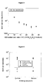
- Figure 4 as contained herein, in this respect clearly shows that with the method in accordance with the present invention etch pit densities can be obtained on germanium surfaces corresponding to the etch pit densities as obtained with the prior art solution, revealing that the method in accordance with the present invention enables the same degree of accuracy with respect to the revealing of etch pits, i.e., defects on the surface.
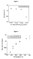
- Figures 1 to 3 as contained herein, furthermore clearly show that within the preferred compositional ratios and within the preferred temperature ranges, highly suitable etch rates can be obtained, securing that the desired effect is obtained without endangering the integrity of GeOl substrate, for example, by delamination.
- the present invention provides a method for treating germanium surfaces, enabling a good control of the etch rates while providing highly satisfactory etch results.
- the present invention enables typically a better control of the etching with results being similar or better, in comparison with the chromium-containing etchant disclosed in the prior art.
- the etch results such as etch pit densities, are similar to densities found with chromium-containing solutions.
- the defects are even better delineated, compared with the chromium-containing prior art etchant, so that even, in addition to the replacement of the undesired chromium-containing etchant, a further advantage is associated with the present invention.
Landscapes
- Physics & Mathematics (AREA)
- Health & Medical Sciences (AREA)
- Life Sciences & Earth Sciences (AREA)
- Chemical & Material Sciences (AREA)
- Analytical Chemistry (AREA)
- Biochemistry (AREA)
- General Health & Medical Sciences (AREA)
- General Physics & Mathematics (AREA)
- Immunology (AREA)
- Pathology (AREA)
- Weting (AREA)
- ing And Chemical Polishing (AREA)
Priority Applications (3)
| Application Number | Priority Date | Filing Date | Title |
|---|---|---|---|
| EP07291590A EP2072994A1 (de) | 2007-12-21 | 2007-12-21 | Verfahren zur Behandlung von Germaniumoberflächen und dabei verwendete Lösungen |
| US12/808,353 US8420548B2 (en) | 2007-12-21 | 2008-11-05 | Method for treating germanium surfaces and solutions to be employed therein |
| PCT/IB2008/003039 WO2009090454A2 (en) | 2007-12-21 | 2008-11-05 | Method for treating germanium surfaces and solutions to be employed therein |
Applications Claiming Priority (1)
| Application Number | Priority Date | Filing Date | Title |
|---|---|---|---|
| EP07291590A EP2072994A1 (de) | 2007-12-21 | 2007-12-21 | Verfahren zur Behandlung von Germaniumoberflächen und dabei verwendete Lösungen |
Publications (1)
| Publication Number | Publication Date |
|---|---|
| EP2072994A1 true EP2072994A1 (de) | 2009-06-24 |
Family
ID=39365434
Family Applications (1)
| Application Number | Title | Priority Date | Filing Date |
|---|---|---|---|
| EP07291590A Withdrawn EP2072994A1 (de) | 2007-12-21 | 2007-12-21 | Verfahren zur Behandlung von Germaniumoberflächen und dabei verwendete Lösungen |
Country Status (3)
| Country | Link |
|---|---|
| US (1) | US8420548B2 (de) |
| EP (1) | EP2072994A1 (de) |
| WO (1) | WO2009090454A2 (de) |
Families Citing this family (1)
| Publication number | Priority date | Publication date | Assignee | Title |
|---|---|---|---|---|
| CN106567079A (zh) * | 2016-09-23 | 2017-04-19 | 中锗科技有限公司 | 一种用于锗单晶片位错检测的腐蚀液及腐蚀方法 |
Citations (1)
| Publication number | Priority date | Publication date | Assignee | Title |
|---|---|---|---|---|
| US3869313A (en) * | 1973-05-21 | 1975-03-04 | Allied Chem | Apparatus for automatic chemical processing of workpieces, especially semi-conductors |
Family Cites Families (2)
| Publication number | Priority date | Publication date | Assignee | Title |
|---|---|---|---|---|
| US3818262A (en) * | 1955-08-04 | 1974-06-18 | Rca Corp | Targets for television pickup tubes |
| FR2864457B1 (fr) * | 2003-12-31 | 2006-12-08 | Commissariat Energie Atomique | Procede de nettoyage par voie humide d'une surface notamment en un materiau de type silicium germanium. |
-
2007
- 2007-12-21 EP EP07291590A patent/EP2072994A1/de not_active Withdrawn
-
2008
- 2008-11-05 US US12/808,353 patent/US8420548B2/en not_active Expired - Fee Related
- 2008-11-05 WO PCT/IB2008/003039 patent/WO2009090454A2/en not_active Ceased
Patent Citations (1)
| Publication number | Priority date | Publication date | Assignee | Title |
|---|---|---|---|---|
| US3869313A (en) * | 1973-05-21 | 1975-03-04 | Allied Chem | Apparatus for automatic chemical processing of workpieces, especially semi-conductors |
Non-Patent Citations (9)
| Title |
|---|
| ABBADIE ET AL.: "comparison of different etching techniques in order to reveal dislocations in thick Ge layers", ECS TRANSACTIONS, vol. 6, no. 4, May 2007 (2007-05-01), chicago (us), pages 263 - 269, XP008091590 * |
| ABBADIE ET AL: "An efficient wet-cleaning of SiGe virtual substrates and of thick, pure Ge layers on Si(001) after a chemical mechanical planarization step", MICROELECTRONIC ENGINEERING, ELSEVIER PUBLISHERS BV., AMSTERDAM, NL, vol. 83, no. 10, 1 October 2006 (2006-10-01), pages 1986 - 1993, XP005510852, ISSN: 0167-9317 * |
| APPLIED PHYSICS LETTERS, vol. 60, no. 7, pages 844 - 846 |
| APPLIED PHYSICS LETTERS, vol. 75, no. 19, pages 2909 - 2911 |
| APPLIED PHYSICS LETTERS, vol. 85, no. 11, pages 1928 - 1930 |
| APPLIED PHYSICS LETTERS, vol. 88, pages 021903 - 1 |
| CLAWSON A R: "Guide to references on III-V semiconductor chemical etching", MATERIALS SCIENCE AND ENGINEERING R: REPORTS, ELSEVIER SEQUOIA S.A., LAUSANNE, CH, vol. 31, no. 1-6, 15 January 2001 (2001-01-15), pages 1 - 438, XP004227677, ISSN: 0927-796X * |
| ECS TRANSACTIONS, vol. 6, no. 4, 2007, pages 263 - 269 |
| JOURNAL OF THE ELECTROCHEMICAL SOCIETY, vol. 119, no. 7, 1972, pages 948 - 951 |
Also Published As
| Publication number | Publication date |
|---|---|
| US20100267244A1 (en) | 2010-10-21 |
| WO2009090454A2 (en) | 2009-07-23 |
| US8420548B2 (en) | 2013-04-16 |
| WO2009090454A3 (en) | 2009-09-03 |
Similar Documents
| Publication | Publication Date | Title |
|---|---|---|
| CN102007394B (zh) | 特别用于应变或应力硅材料的刻蚀组合物、表征这种材料表面上的缺陷的方法,和用刻蚀组合物处理这种表面的工艺 | |
| KR100930294B1 (ko) | Si-기판 및 SiGe-기판을 위한 크롬이 없는 식각용액, 상기 식각 용액을 이용하여 결함을 나타내기위한방법 및 상기 식각 용액을 이용하여 Si-기판 및SiGe-기판을 처리하기 위한 프로세스 | |
| TWI404134B (zh) | 半導體裝置之製造方法及半導體表面上之微型粗糙度之降低方法 | |
| EP1883104B1 (de) | Verfahren zur Herstellung eines gebundenen SOI-Wafers | |
| JP2008131052A6 (ja) | Si基板およびSiGe基板用のクロムを含まないエッチング液、そのエッチング液を使用して欠陥を明らかにする方法、およびそのエッチング液を使用してSi基板およびSiGe基板を処理するプロセス | |
| TWI678601B (zh) | 可抑制含鎢材料之損壞的半導體元件之清洗液及利用該清洗液的半導體元件之清洗方法 | |
| TWI434149B (zh) | 洗淨用組成物、半導體元件之製法 | |
| KR101770754B1 (ko) | 금속 배선 식각액 및 이를 이용한 액정 표시 장치의 제조 방법 | |
| US7579309B2 (en) | Methods for characterizing defects on silicon surfaces and etching composition and treatment process therefor | |
| WO2012031453A1 (zh) | 一种含氟清洗液 | |
| JP2008118138A6 (ja) | シリコン表面上の欠陥を特徴付ける方法、シリコン表面用のエッチング組成物、およびシリコン表面をエッチング組成物で処理するプロセス | |
| WO2009052707A1 (fr) | Composition de nettoyage de résidus de gravure au plasma | |
| US8420548B2 (en) | Method for treating germanium surfaces and solutions to be employed therein | |
| EP1542080A1 (de) | Zusammensetzung zur Entfernung von Photoresistrückständen | |
| EP1909309A1 (de) | Verfahren zur herstellung eines simox-wafers und durch ein solches verfahren hergestellter simox-wafer | |
| KR20050003163A (ko) | 질화물 제거용 식각액 및 이를 이용한 반도체 소자의질화막 제거방법 | |
| JP2017098502A (ja) | エッチング方法 | |
| EP2226374B1 (de) | Ätzzusammensetzung, insbesondere für Siliciummaterialien, Verfahren zur Charakterisierung von Fehlern derartiger Materialien und Verfahren zur Behandlung derartiger Oberflächen mit der Ätzzusammensetzung | |
| CN111902569A (zh) | 蚀刻液 | |
| TWI759450B (zh) | 蝕刻液、蝕刻方法、及顯示裝置之製造方法 | |
| KR101621546B1 (ko) | 액정표시장치용 어레이 기판의 제조 방법 | |
| KR100520507B1 (ko) | 반도체 소자의 티타늄알루미나이드 검사를 위한 알루미늄제거용 화학용액 | |
| WO2023032488A1 (ja) | シリコンウェーハの洗浄方法および製造方法 | |
| Luo et al. | Method to Reduce Crystal Defects in AlCu Bond Pad | |
| KR20110016724A (ko) | 금속 배선 형성을 위한 식각액 조성물 |
Legal Events
| Date | Code | Title | Description |
|---|---|---|---|
| PUAI | Public reference made under article 153(3) epc to a published international application that has entered the european phase |
Free format text: ORIGINAL CODE: 0009012 |
|
| AK | Designated contracting states |
Kind code of ref document: A1 Designated state(s): AT BE BG CH CY CZ DE DK EE ES FI FR GB GR HU IE IS IT LI LT LU LV MC MT NL PL PT RO SE SI SK TR |
|
| AX | Request for extension of the european patent |
Extension state: AL BA HR MK RS |
|
| 17P | Request for examination filed |
Effective date: 20090714 |
|
| RAP1 | Party data changed (applicant data changed or rights of an application transferred) |
Owner name: S.O.I.TEC SILICON ON INSULATOR TECHNOLOGIES |
|
| 17Q | First examination report despatched |
Effective date: 20091030 |
|
| AKX | Designation fees paid |
Designated state(s): AT BE BG CH CY CZ DE DK EE ES FI FR GB GR HU IE IS IT LI LT LU LV MC MT NL PL PT RO SE SI SK TR |
|
| RAP1 | Party data changed (applicant data changed or rights of an application transferred) |
Owner name: SOITEC |
|
| STAA | Information on the status of an ep patent application or granted ep patent |
Free format text: STATUS: THE APPLICATION IS DEEMED TO BE WITHDRAWN |
|
| 18D | Application deemed to be withdrawn |
Effective date: 20140701 |