EP2073023A2 - Composant micromécanique doté d'un élément orientable - Google Patents
Composant micromécanique doté d'un élément orientable Download PDFInfo
- Publication number
- EP2073023A2 EP2073023A2 EP08105758A EP08105758A EP2073023A2 EP 2073023 A2 EP2073023 A2 EP 2073023A2 EP 08105758 A EP08105758 A EP 08105758A EP 08105758 A EP08105758 A EP 08105758A EP 2073023 A2 EP2073023 A2 EP 2073023A2
- Authority
- EP
- European Patent Office
- Prior art keywords
- layer
- micromechanical component
- deflectable
- functional layer
- component according
- Prior art date
- Legal status (The legal status is an assumption and is not a legal conclusion. Google has not performed a legal analysis and makes no representation as to the accuracy of the status listed.)
- Ceased
Links
Images




Classifications
-
- G—PHYSICS
- G01—MEASURING; TESTING
- G01P—MEASURING LINEAR OR ANGULAR SPEED, ACCELERATION, DECELERATION, OR SHOCK; INDICATING PRESENCE, ABSENCE, OR DIRECTION, OF MOVEMENT
- G01P15/00—Measuring acceleration; Measuring deceleration; Measuring shock, i.e. sudden change of acceleration
- G01P15/02—Measuring acceleration; Measuring deceleration; Measuring shock, i.e. sudden change of acceleration by making use of inertia forces using solid seismic masses
- G01P15/08—Measuring acceleration; Measuring deceleration; Measuring shock, i.e. sudden change of acceleration by making use of inertia forces using solid seismic masses with conversion into electric or magnetic values
- G01P15/125—Measuring acceleration; Measuring deceleration; Measuring shock, i.e. sudden change of acceleration by making use of inertia forces using solid seismic masses with conversion into electric or magnetic values by capacitive pick-up
-
- G—PHYSICS
- G01—MEASURING; TESTING
- G01P—MEASURING LINEAR OR ANGULAR SPEED, ACCELERATION, DECELERATION, OR SHOCK; INDICATING PRESENCE, ABSENCE, OR DIRECTION, OF MOVEMENT
- G01P1/00—Details of instruments
- G01P1/02—Housings
- G01P1/023—Housings for acceleration measuring devices
-
- G—PHYSICS
- G01—MEASURING; TESTING
- G01P—MEASURING LINEAR OR ANGULAR SPEED, ACCELERATION, DECELERATION, OR SHOCK; INDICATING PRESENCE, ABSENCE, OR DIRECTION, OF MOVEMENT
- G01P15/00—Measuring acceleration; Measuring deceleration; Measuring shock, i.e. sudden change of acceleration
- G01P15/02—Measuring acceleration; Measuring deceleration; Measuring shock, i.e. sudden change of acceleration by making use of inertia forces using solid seismic masses
- G01P15/08—Measuring acceleration; Measuring deceleration; Measuring shock, i.e. sudden change of acceleration by making use of inertia forces using solid seismic masses with conversion into electric or magnetic values
- G01P15/0802—Details
-
- G—PHYSICS
- G01—MEASURING; TESTING
- G01P—MEASURING LINEAR OR ANGULAR SPEED, ACCELERATION, DECELERATION, OR SHOCK; INDICATING PRESENCE, ABSENCE, OR DIRECTION, OF MOVEMENT
- G01P15/00—Measuring acceleration; Measuring deceleration; Measuring shock, i.e. sudden change of acceleration
- G01P15/02—Measuring acceleration; Measuring deceleration; Measuring shock, i.e. sudden change of acceleration by making use of inertia forces using solid seismic masses
- G01P15/08—Measuring acceleration; Measuring deceleration; Measuring shock, i.e. sudden change of acceleration by making use of inertia forces using solid seismic masses with conversion into electric or magnetic values
- G01P2015/0805—Measuring acceleration; Measuring deceleration; Measuring shock, i.e. sudden change of acceleration by making use of inertia forces using solid seismic masses with conversion into electric or magnetic values being provided with a particular type of spring-mass-system for defining the displacement of a seismic mass due to an external acceleration
- G01P2015/0822—Measuring acceleration; Measuring deceleration; Measuring shock, i.e. sudden change of acceleration by making use of inertia forces using solid seismic masses with conversion into electric or magnetic values being provided with a particular type of spring-mass-system for defining the displacement of a seismic mass due to an external acceleration for defining out-of-plane movement of the mass
- G01P2015/0825—Measuring acceleration; Measuring deceleration; Measuring shock, i.e. sudden change of acceleration by making use of inertia forces using solid seismic masses with conversion into electric or magnetic values being provided with a particular type of spring-mass-system for defining the displacement of a seismic mass due to an external acceleration for defining out-of-plane movement of the mass for one single degree of freedom of movement of the mass
- G01P2015/0831—Measuring acceleration; Measuring deceleration; Measuring shock, i.e. sudden change of acceleration by making use of inertia forces using solid seismic masses with conversion into electric or magnetic values being provided with a particular type of spring-mass-system for defining the displacement of a seismic mass due to an external acceleration for defining out-of-plane movement of the mass for one single degree of freedom of movement of the mass the mass being of the paddle type having the pivot axis between the longitudinal ends of the mass, e.g. see-saw configuration
Definitions
- the invention is based on a micromechanical component according to the preamble of the main claim.
- An acceleration sensor which has a rocker.
- the rocker is connected to a wafer so via torsion bars that an asymmetric and outside the center of gravity of the rocker extending axis of rotation is formed.
- a disadvantage of the acceleration sensor is that in a differential capacitive determination of the deflection of the rocker, the asymmetric suspension of the rocker leads to measurement inaccuracies.
- micromechanical device according to the invention according to the main claim or the features of the independent claims has the advantage that no asymmetric suspension of the deflectable element must be provided.
- the measurement accuracy and the measuring sensitivity of the micromechanical component can be improved in an advantageous manner.
- the deflectable element is subdivided by a plane into a first subarea and into a second subarea.
- the plane in this case runs essentially perpendicular to the main extension plane of the deflectable element and substantially centrally through the suspension element.
- the first subarea has a greater mass moment of inertia than the second subarea.
- the base of the deflectable element which is the Substrate material is arranged, divided by the plane into two substantially equal surface areas. Since the plane extends centrally through the suspension element, the suspension element is arranged substantially symmetrically to the base. The plane is substantially perpendicular to the base of the deflectable element.
- the first partial area and the second partial area have on average the same distance to a rotation axis.
- the different moments of inertia of the first and the second partial area may arise due to a different outer contour of the first partial area relative to the second partial area and / or by the presence of different material densities in the first partial area relative to the second partial area and / or by different masses of the first and second subarea.
- the first subarea preferably has a height perpendicular to the main extension plane of the deflectable element which is greater than the height of the second subarea perpendicular to the main extension plane of the deflectable element. Preferably, this creates a step in the deflectable element.
- the first subregion has a greater mass than the second subregion, if the material densities of the first subregion and of the second subregion are substantially the same.
- the deflection of the deflectable element can be determined by means of a differential capacitance measurement.
- the micromechanical component preferably has a cover element.
- a cap wafer can be used as the cover element.
- the micromechanical component likewise has a deflectable element, wherein here too the deflectable element is connected to a substrate material by means of a suspension element.
- the micromechanical component has a Cover element, wherein the deflection of the deflectable element can be determined by means of a differential capacitance measurement.
- the cover element has for this purpose a conductive layer as a counter electrode.
- the deflectable element and / or a substrate material or a layer on the deflectable element and / or the substrate material preferably forms an electrode, so that an electrode-counterelectrode pair is formed with the cover element.
- the deflectable element likewise has a first partial region and a second partial region in the abovementioned other embodiment, wherein the first partial region has a greater mass moment of inertia than the second partial region.
- the plane preferably divides the base area into two essentially equal areas or the plane divides the base area into two areas of different size.
- the suspension element is arranged asymmetrically with respect to the base of the oscillatory element. The deflectable element is thus suspended asymmetrically on the substrate material.
- the different mass moment of inertia is preferably formed as in the first embodiment.
- the different mass moment of inertia preferably results from the fact that the first partial area is on the center farther from the axis of rotation than the second partial area.
- the first partial region and the second partial region preferably have substantially the same material density, but the first partial region has a mass which corresponds at least to the mass of the second partial region.
- the micromechanical component preferably has a back contact.
- the rear-side contacting of the micromechanical component advantageously allows the use of unstructured cover elements for covering the micromechanical component.
- a unstructured Pyrex wafer can be used as the cover element.
- electrical contacting of the micromechanical component is possible due to the rear-side contacting.
- the production of a cover element is thus advantageously simplified.
- the rear-side contact is usually carried out by a thinning of a precursor of the micromechanical device, whereby advantageously the height of the micromechanical device is reduced.
- the micromechanical component preferably has a first and / or a second functional layer.
- the first and / or the second functional layer are preferably epitaxial polysilicon layers.
- the micromechanical component is preferably in contact with the cover element by means of a contact means.
- the contact means is conductive. If the cover element has a conductive layer or is itself made of conductive material, then an electrical contacting of the conductive layer can be produced by the conductive contact means.
- the contact means may be connected to the conductive layer of the cover element and to a bonding frame, wherein the bonding frame is electrically contacted.
- the use of non-conductive material as a contact means is possible.
- the direct attachment of the cover element to the is preferred Micromechanical device, for example by anodic bonding, possible.
- the preferred contact means is a material or combination of materials whose melting temperature and / or eutectic point is in the temperature range of about 170 ° C to 600 ° C.
- the micromechanical component is preferably used as an acceleration sensor.
- the person skilled in the art will understand that the acceleration is determined by the force of inertia acting on the deflectable element.
- Particularly preferred is a Z-acceleration sensor.
- Another object of the present invention is a method for producing the micromechanical device.
- a first insulation layer and / or a first contacting layer is produced, wherein a protective layer is produced at least partially over the first insulation layer and / or over the first contacting layer.
- a first functional layer, a first mask layer and a second functional layer are produced over the first insulating layer and / or the first contacting layer and the protective layer.
- the mask layer lies between the first and the second functional layer, and the first functional layer lies below the second functional layer, as viewed from a first side of the substrate material.
- a "buried mask" can be formed by means of which, for example, the greater mass moment of inertia of the first subregion can be formed relative to the moment of inertia of the second subregion.
- a second contacting layer is formed on partial regions of the second functional layer and / or a second mask layer is produced on the second functional layer and / or over the second contacting layer, at least on sections.
- a further contacting possibility of the micromechanical component is thus possible by means of the second contacting layer.
- trench structures are produced in a trench process, wherein the trench process is stopped by reaching the first mask layer and / or by reaching the protective layer.
- the different mass moment of inertia of the first and the second subarea may be formed, since some sections of the second functional layer (not covered by the second mask layer) are removed by the trenching process and other sections (covered by the second masking layer) do not pass through the trench process are removed.
- sections of the first and / or the second functional layer, which later form the deflectable element are also perforated in a targeted manner.
- an etching step follows, wherein the protective layer is at least partially removed in the etching step.
- the deflectable element is preferably deflectable. The removal of the protective layer below the deflectable element to be formed is facilitated by the perforation of the first and / or the second functional layer.
- a cover element is attached directly or indirectly to or with the first or on or with the second functional layer.
- An indirect attachment of the cover element is intended to be understood when the cover element is connected by means of a contact means with the first or the second functional layer.
- the cover element preferably has a conductive layer, for example aluminum. However, it is also conceivable that the cover element has no conductive layer.
- the cover element is preferably a Pyrex cap wafer and / or is structured or unstructured.
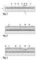
- FIGS. 1 to 6 schematically a first embodiment of a precursor of a micromechanical device is shown.
- FIG. 7 schematically a second embodiment of a precursor of the micromechanical device is shown.
- FIG. 8 schematically shows a preliminary stage of the first embodiment of the micromechanical device with a cover member and rear side contact.
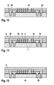
- FIGS. 9 to 16 schematically shows a method for producing a micromechanical device with back contact and various electrode configurations / - embodiments shown.
- FIG. 17 is schematically illustrated an embodiment of a deflectable element with different mass moments of inertia in a first portion and in a second portion.
- FIG. 1 schematically a precursor 1 of a micromechanical device is shown, wherein the precursor 1, a substrate material 3, a first insulating layer 12 and a first contacting layer 13 has.
- the first insulating layer 12 and the first contacting layer 13 are preferably produced on a first side of the substrate material 3.
- the first insulation layer 12 has been produced substantially over the entire area of the substrate material.
- the first contacting layer 13 has been produced over portions of the first insulating layer 12. This results in recesses 32 in the first contacting layer 13.
- a protective layer 14 has been produced, which likewise has recesses 31.
- the protective layer 14 thereby passes into the recesses 32 of the first contacting layer.
- a first functional layer 9 is produced.
- a first mask layer 15 is produced in sections on the first functional layer 9.
- the substrate material 3 is preferably silicon, the first insulation layer 12 silicon oxide, the first contact layer 13 polysilicon, the protective layer 14 silicon oxide, the first functional layer 9 EPI (epitaxial polysilicon) and the first mask layer 15 silicon oxide.
- FIG. 2 schematically shows that a second functional layer 10 has been generated over the first mask layer 15 and the first functional layer 9.
- the second functional layer 10 is preferably made of EPI.
- the first mask layer 15 is buried by the second functional layer 10.
- a second contacting layer 17 is preferably produced in sections over the second functional layer 10. Both the functional layers 9 and 10 and the contacting layer 13 can be doped and / or deposited undoped.
- a second mask layer 18 is generated schematically over sections of the second functional layer 10 and over the second contacting layer 17.
- trench structures in the precursor 1 of the micromechanical device and targeted perforation or perforated regions 22 in the deflectable element 2 to be produced can advantageously be produced later.
- the protective layer 14 can advantageously be removed more easily in a subsequent etching step.
- the precursor 1 of the micromechanical device is shown after an etching step.
- the etching step is preferably an HF gas phase etching.
- the Etching agent is preferably the protective layer 14 removed from the regions 20 and the first mask layer 15 has been removed. Through the recess 31 of the protective layer 14 in this case a suspension element 4 has been formed.
- the removal of the protective layer 14 results in a deflectable element 2, since the deflectable element 2 is in contact only with the substrate material 3 or with the first contacting layer 13 through the suspension element 4.
- the deflectable element 2 is deflectable about an axis of rotation 5, which extends through the suspension element 4.
- the axis of rotation 5 is in the FIG. 5 indicated schematically and extends perpendicular to the plane.
- the FIGS. 1 to 16 otherwise represent sectional representations of the precursor 1 of the micromechanical device.
- the suspension element 4 can be arranged substantially centrally to a base surface 36 of the oscillatory element 2, as in FIG. 17 shown schematically.
- This base surface 36 is facing the substrate material 3 and is divided by the suspension element 4 or a plane 35.
- the surface areas of the base area 36 that are divided by the suspension element 4 are substantially the same size.
- the formation of the stage determines the exact position of the suspension element 4.
- FIG. 6 the micromechanical component is shown with a cover element 6.
- the cover element 6 is connected by means of a contact means 11 with supports 21.
- the supports 21 preferably form a Bonding frame off.
- the points of the first contacting layer 13 identified by the arrows preferably serve as individual electrodes 7 in this structure.
- the deflectable element 2 itself serves as a counterelectrode. In the case of a deflection of the deflectable element 2 about the axis of rotation 5, the end regions of the deflectable element 2 arrive at a different distance from the two electrodes 7, which are formed by the first contacting layer 13. In each case between an electrode 7 and the deflectable element 2 while the capacitance is measured. It is thus possible to measure the difference capacitance.
- FIG. 7 schematically another embodiment of the micromechanical device is shown.
- the suspension member 4 is arranged asymmetrically with respect to the main extension plane of the deflectable member 2.
- the micromechanical component is in contact with a cover element 6, the cover element 6 being connected to the supports 21 by means of contact means 11.
- the supports 21 are preferably formed by the first and / or the second functional layer 9, 10.
- the cover element 6 preferably has a conductive layer 8-for example an aluminum layer-and a second insulation layer 23.
- the contacting of the electrically conductive layer 8 is preferably carried out by an electrical connection of the bonding frame (formed by the supports 21) to the substrate material 3 and / or the contacting layer 13 by an electrically conductive contact means 11.
- the conductive layer 8 forms a counter electrode 16 in this embodiment.
- the first contacting layer 13 below the deflectable element 2 preferably forms the electrode 7 and the deflectable element 2 itself preferably forms a center electrode.
- the distance between the counterelectrode 16 of the cover element 6 and the center electrode of the deflectable element 2 and between the electrode 7 of the first contacting layer 13 and the deflectable element 2 changes.
- the cover element 6 can also be changed consist of highly doped silicon and be connected via the bond and the bonding frame with the substrate material 3 and / or the contacting layer 13. In this case, it is not necessary that the cover member 6 has an additional conductive layer 8 to be effective as a counter electrode 16.
- a further alternative would be a silicon cap of any doping as cover element 6, on which a metallization is deposited directly, the metallization being optionally structured.
- FIGS. 8 to 16 schematically represent a back side contacting a precursor 1 of the micromechanical device.
- the micromechanical device preferably has a third insulating layer 24 and a contact 25 on.
- the first functional layer 9 has to be designed in accordance with FIG FIG. 9 be structured. This results in first contact regions 26 between which the deflectable element 2 formed later lies.
- the first functional layer 9 also passes into recesses 28 of the substrate material 3, wherein the first functional layer 9 is preferably an insulator.
- the recesses 28 are preferably formed by a process step (for example trenches) prior to the application of the first insulating layer 12 and the first contacting layer 13. After the generation of trench structures 19 (FIG. FIG.
- the second contact areas 29 are formed by the subsequent removal of the protective layer 14 from the areas 20, the deflectable element 2 is formed, wherein a fixed counter electrode 16 through the second functional layer 10 is formed.
- the electrode 7 is formed below the deflectable element 2 through the protective layer 13, wherein also here two different and non-contiguous portions of the protective layer 13 each form an electrode 7.
- the deflectable element 2 forms the movable center electrode.
- the third insulation layer 24 and the contacting 25 are then produced on the substrate material 3 ( FIG. 12 ). Since the contacting of the micromechanical component takes place from the rear side, advantageously an unstructured cover element 6, for example a Pyrex cap wafer, can be used to cover the micromechanical device.
- FIG. 13 to 16 schematically show further embodiments of the micromechanical device with back side contacting, for example, a cover member 6 is in contact with a conductive layer 8 with the micromechanical device or a contact means 11 between the cover member 6 and the substrate material 3 is provided.
- FIG. 14 is schematically shown that 10 different contacting areas were created by the second functional layer.
- a cover element 6 which additionally has a conductive layer 8, to the functional layer 9 or 10
- an electrically insulating connection in the region of the bonding frame and an electrically conductive connection within the inner space enclosed by the bonding frame can simultaneously arise.
- the attachment of a covering element 6 made of Pyrex is here called, which is connected by anodic bonding electrically non-conductive with the functional layer 9 or 10.
- this cover element 6 additionally possesses an electrically conductive layer 8, for example of aluminum, an electrically conductive connection to isolated regions in the functional layer 9 and / or 10 can be created in the same connection process. Since the cover element 6 comes to lie directly on the functional layer 9 or 10 in the case of anodic bonding, a depression must be introduced into the functional layer 9 or 10 in the region of the movable structures (deflectable element 2) in order to be able to ensure the mobility of the deflectable element 2 , This is not absolutely necessary when using electrically conductive or non-conductive contact means, since these are already too a spacing between cover element 6 and functional layer 9 or 10 leads.
- FIG. 17 schematically represents the deflectable element 2, wherein a first portion 33 of the deflectable element 2 and a second portion 34 of the deflectable element 2 form a step.
- the first subregion 33 has a height perpendicular to the main extension plane of the deflectable element 2 which is greater than the height of the second subregion 34 perpendicular to the main extension plane of the deflectable element 2.
- 34 to the axis of rotation 5 thus has the first portion 34 (in the FIG. 17 to the left of the axis of rotation 5) has a greater mass moment of inertia than the second portion 34 (in the FIG.
- a plane 35 is substantially perpendicular to the base surface 36 of the deflectable element 2, wherein the base surface 36 is in contact with the substrate material 3 via the suspension element 4 and faces the substrate material 3.
- the plane 35 divides the base 36 into two substantially equal areas, the deflectable element 2 is suspended substantially centrally by the suspension element 4.
Landscapes
- Physics & Mathematics (AREA)
- General Physics & Mathematics (AREA)
- Micromachines (AREA)
Applications Claiming Priority (1)
| Application Number | Priority Date | Filing Date | Title |
|---|---|---|---|
| DE200710061096 DE102007061096A1 (de) | 2007-12-19 | 2007-12-19 | Mikromechanisches Bauelement mit auslenkfähigem Element |
Publications (2)
| Publication Number | Publication Date |
|---|---|
| EP2073023A2 true EP2073023A2 (fr) | 2009-06-24 |
| EP2073023A3 EP2073023A3 (fr) | 2012-05-09 |
Family
ID=40491028
Family Applications (1)
| Application Number | Title | Priority Date | Filing Date |
|---|---|---|---|
| EP08105758A Ceased EP2073023A3 (fr) | 2007-12-19 | 2008-11-11 | Composant micromécanique doté d'un élément orientable |
Country Status (2)
| Country | Link |
|---|---|
| EP (1) | EP2073023A3 (fr) |
| DE (1) | DE102007061096A1 (fr) |
Citations (1)
| Publication number | Priority date | Publication date | Assignee | Title |
|---|---|---|---|---|
| DE19541388A1 (de) | 1995-11-07 | 1997-05-15 | Telefunken Microelectron | Mikromechanischer Beschleunigungssensor |
Family Cites Families (10)
| Publication number | Priority date | Publication date | Assignee | Title |
|---|---|---|---|---|
| DE3824695A1 (de) * | 1988-07-20 | 1990-02-01 | Fraunhofer Ges Forschung | Mikromechanischer beschleunigungssensor mit kapazitiver signalwandlung und verfahren zu seiner herstellung |
| US6073484A (en) * | 1995-07-20 | 2000-06-13 | Cornell Research Foundation, Inc. | Microfabricated torsional cantilevers for sensitive force detection |
| US6230566B1 (en) * | 1999-10-01 | 2001-05-15 | The Regents Of The University Of California | Micromachined low frequency rocking accelerometer with capacitive pickoff |
| DE10065013B4 (de) * | 2000-12-23 | 2009-12-24 | Robert Bosch Gmbh | Verfahren zum Herstellen eines mikromechanischen Bauelements |
| DE60232250D1 (de) * | 2001-08-20 | 2009-06-18 | Honeywell Int Inc | Bogenförmige federelemente für mikro-elektromechanischen beschleunigungssensor |
| US7140250B2 (en) * | 2005-02-18 | 2006-11-28 | Honeywell International Inc. | MEMS teeter-totter accelerometer having reduced non-linearty |
| US7268463B2 (en) * | 2005-07-28 | 2007-09-11 | Freescale Semiconductor, Inc. | Stress release mechanism in MEMS device and method of making same |
| DE102007019647A1 (de) | 2007-04-26 | 2008-10-30 | Robert Bosch Gmbh | Verfahren zur Herstellung eines mikromechanischen Bauelements mit Auffüllschicht und Maskenschicht |
| DE102007019638A1 (de) | 2007-04-26 | 2008-10-30 | Robert Bosch Gmbh | Verfahren zur Herstellung eines mikromechanischen Bauelements mit Trenchstruktur zur Rückseitenkontaktierung |
| US8122767B2 (en) * | 2008-10-08 | 2012-02-28 | Honeywell International Inc. | D'arsonval movement mems accelerometer |
-
2007
- 2007-12-19 DE DE200710061096 patent/DE102007061096A1/de not_active Ceased
-
2008
- 2008-11-11 EP EP08105758A patent/EP2073023A3/fr not_active Ceased
Patent Citations (1)
| Publication number | Priority date | Publication date | Assignee | Title |
|---|---|---|---|---|
| DE19541388A1 (de) | 1995-11-07 | 1997-05-15 | Telefunken Microelectron | Mikromechanischer Beschleunigungssensor |
Also Published As
| Publication number | Publication date |
|---|---|
| DE102007061096A1 (de) | 2009-06-25 |
| EP2073023A3 (fr) | 2012-05-09 |
Similar Documents
| Publication | Publication Date | Title |
|---|---|---|
| DE19537814B4 (de) | Sensor und Verfahren zur Herstellung eines Sensors | |
| DE102007060878B4 (de) | Mikromechanisches System | |
| DE69305955T2 (de) | Beschleunigungssensor und seine herstellung | |
| DE10065013B4 (de) | Verfahren zum Herstellen eines mikromechanischen Bauelements | |
| DE102008043524B4 (de) | Beschleunigungssensor und Verfahren zu seiner Herstellung | |
| DE102014223886B4 (de) | MEMS-Vorrichtung | |
| DE102008043788A1 (de) | Mikromechanisches Bauelement | |
| EP2331453B1 (fr) | Composant micro-mécanique ayant une electrode traversante et procédé de production associé | |
| EP0773443A1 (fr) | Accéléromètre micro-usine | |
| DE19906067A1 (de) | Halbleitersensor für physikalische Größen und dessen Herstellungsverfahren | |
| DE102014215038B4 (de) | Mikromechanischer Sensor und Verfahren zur Herstellung eines mikromechanischen Sensors | |
| DE102013208825A1 (de) | Mikrostrukturbauelement und Verfahren zur Herstellung eines Mikrostrukturbauelements | |
| DE102019202794B3 (de) | Mikromechanische Sensorvorrichtung und entsprechendes Herstellungsverfahren | |
| DE102013216901A1 (de) | Mikromechanisches Bauelement und Verfahren zur Herstellung eines mikromechanischen Bauelements | |
| DE102015212669B4 (de) | Kapazitive mikroelektromechanische Vorrichtung und Verfahren zum Ausbilden einer kapazitiven mikroelektromechanischen Vorrichtung | |
| DE102010061782B4 (de) | Verfahren zum Herstellen eines mikromechanischen Bauelements | |
| DE19817311B4 (de) | Herstellungsverfahren für mikromechanisches Bauelement | |
| DE102010029709B4 (de) | Mikromechanisches Bauelement und Verfahren zum Herstellen eines mikromechanischen Bauelements | |
| EP0950190A1 (fr) | Ensemble micromecanique a semiconducteur et procede de production correspondant | |
| DE10303751A1 (de) | Kapazitiver Sensor für eine dynamische Größe | |
| DE10310339A1 (de) | Verfahren zum Herstellen einer Halbleitervorrichtung | |
| DE102013001674A1 (de) | Vertikale druckempfindliche Struktur | |
| DE10196677B4 (de) | Elektrodenstruktur und Verfahren zum Herstellen eines Dünnschicht-Strukturkörpers | |
| EP2073023A2 (fr) | Composant micromécanique doté d'un élément orientable | |
| EP2150488B1 (fr) | Procédé de fabrication d'un composant micromécanique comportant une couche de charge et une couche de masque |
Legal Events
| Date | Code | Title | Description |
|---|---|---|---|
| PUAI | Public reference made under article 153(3) epc to a published international application that has entered the european phase |
Free format text: ORIGINAL CODE: 0009012 |
|
| AK | Designated contracting states |
Kind code of ref document: A2 Designated state(s): AT BE BG CH CY CZ DE DK EE ES FI FR GB GR HR HU IE IS IT LI LT LU LV MC MT NL NO PL PT RO SE SI SK TR |
|
| AX | Request for extension of the european patent |
Extension state: AL BA MK RS |
|
| RIC1 | Information provided on ipc code assigned before grant |
Ipc: G01P 15/125 20060101ALI20111214BHEP Ipc: G01P 15/08 20060101AFI20111214BHEP Ipc: G01P 1/02 20060101ALI20111214BHEP |
|
| PUAL | Search report despatched |
Free format text: ORIGINAL CODE: 0009013 |
|
| RIN1 | Information on inventor provided before grant (corrected) |
Inventor name: WEBER, HERIBERT Inventor name: TEBJE, LARS Inventor name: SCHEUERER, ROLAND |
|
| AK | Designated contracting states |
Kind code of ref document: A3 Designated state(s): AT BE BG CH CY CZ DE DK EE ES FI FR GB GR HR HU IE IS IT LI LT LU LV MC MT NL NO PL PT RO SE SI SK TR |
|
| AX | Request for extension of the european patent |
Extension state: AL BA MK RS |
|
| RIC1 | Information provided on ipc code assigned before grant |
Ipc: G01P 15/08 20060101AFI20120405BHEP Ipc: G01P 15/125 20060101ALI20120405BHEP Ipc: G01P 1/02 20060101ALI20120405BHEP |
|
| 17P | Request for examination filed |
Effective date: 20121109 |
|
| AKX | Designation fees paid |
Designated state(s): DE FR IT |
|
| STAA | Information on the status of an ep patent application or granted ep patent |
Free format text: STATUS: EXAMINATION IS IN PROGRESS |
|
| 17Q | First examination report despatched |
Effective date: 20171214 |
|
| APBK | Appeal reference recorded |
Free format text: ORIGINAL CODE: EPIDOSNREFNE |
|
| APBN | Date of receipt of notice of appeal recorded |
Free format text: ORIGINAL CODE: EPIDOSNNOA2E |
|
| APBR | Date of receipt of statement of grounds of appeal recorded |
Free format text: ORIGINAL CODE: EPIDOSNNOA3E |
|
| APAF | Appeal reference modified |
Free format text: ORIGINAL CODE: EPIDOSCREFNE |
|
| RAP1 | Party data changed (applicant data changed or rights of an application transferred) |
Owner name: ROBERT BOSCH GMBH |
|
| P01 | Opt-out of the competence of the unified patent court (upc) registered |
Effective date: 20230509 |
|
| APBT | Appeal procedure closed |
Free format text: ORIGINAL CODE: EPIDOSNNOA9E |
|
| STAA | Information on the status of an ep patent application or granted ep patent |
Free format text: STATUS: THE APPLICATION HAS BEEN REFUSED |
|
| 18R | Application refused |
Effective date: 20240701 |