EP2073054A2 - Anzeigevorrichtung - Google Patents
Anzeigevorrichtung Download PDFInfo
- Publication number
- EP2073054A2 EP2073054A2 EP08171628A EP08171628A EP2073054A2 EP 2073054 A2 EP2073054 A2 EP 2073054A2 EP 08171628 A EP08171628 A EP 08171628A EP 08171628 A EP08171628 A EP 08171628A EP 2073054 A2 EP2073054 A2 EP 2073054A2
- Authority
- EP
- European Patent Office
- Prior art keywords
- wiring line
- terminal
- terminal wiring
- contact hole
- metal layer
- Prior art date
- Legal status (The legal status is an assumption and is not a legal conclusion. Google has not performed a legal analysis and makes no representation as to the accuracy of the status listed.)
- Granted
Links
Images


Classifications
-
- G—PHYSICS
- G02—OPTICS
- G02F—OPTICAL DEVICES OR ARRANGEMENTS FOR THE CONTROL OF LIGHT BY MODIFICATION OF THE OPTICAL PROPERTIES OF THE MEDIA OF THE ELEMENTS INVOLVED THEREIN; NON-LINEAR OPTICS; FREQUENCY-CHANGING OF LIGHT; OPTICAL LOGIC ELEMENTS; OPTICAL ANALOGUE/DIGITAL CONVERTERS
- G02F1/00—Devices or arrangements for the control of the intensity, colour, phase, polarisation or direction of light arriving from an independent light source, e.g. switching, gating or modulating; Non-linear optics
- G02F1/01—Devices or arrangements for the control of the intensity, colour, phase, polarisation or direction of light arriving from an independent light source, e.g. switching, gating or modulating; Non-linear optics for the control of the intensity, phase, polarisation or colour
- G02F1/13—Devices or arrangements for the control of the intensity, colour, phase, polarisation or direction of light arriving from an independent light source, e.g. switching, gating or modulating; Non-linear optics for the control of the intensity, phase, polarisation or colour based on liquid crystals, e.g. single liquid crystal display cells
- G02F1/133—Constructional arrangements; Operation of liquid crystal cells; Circuit arrangements
- G02F1/1333—Constructional arrangements; Manufacturing methods
- G02F1/1345—Conductors connecting electrodes to cell terminals
- G02F1/13452—Conductors connecting driver circuitry and terminals of panels
-
- G—PHYSICS
- G02—OPTICS
- G02F—OPTICAL DEVICES OR ARRANGEMENTS FOR THE CONTROL OF LIGHT BY MODIFICATION OF THE OPTICAL PROPERTIES OF THE MEDIA OF THE ELEMENTS INVOLVED THEREIN; NON-LINEAR OPTICS; FREQUENCY-CHANGING OF LIGHT; OPTICAL LOGIC ELEMENTS; OPTICAL ANALOGUE/DIGITAL CONVERTERS
- G02F1/00—Devices or arrangements for the control of the intensity, colour, phase, polarisation or direction of light arriving from an independent light source, e.g. switching, gating or modulating; Non-linear optics
- G02F1/01—Devices or arrangements for the control of the intensity, colour, phase, polarisation or direction of light arriving from an independent light source, e.g. switching, gating or modulating; Non-linear optics for the control of the intensity, phase, polarisation or colour
- G02F1/13—Devices or arrangements for the control of the intensity, colour, phase, polarisation or direction of light arriving from an independent light source, e.g. switching, gating or modulating; Non-linear optics for the control of the intensity, phase, polarisation or colour based on liquid crystals, e.g. single liquid crystal display cells
- G02F1/133—Constructional arrangements; Operation of liquid crystal cells; Circuit arrangements
- G02F1/1333—Constructional arrangements; Manufacturing methods
- G02F1/1345—Conductors connecting electrodes to cell terminals
- G02F1/13458—Terminal pads
-
- G—PHYSICS
- G09—EDUCATION; CRYPTOGRAPHY; DISPLAY; ADVERTISING; SEALS
- G09G—ARRANGEMENTS OR CIRCUITS FOR CONTROL OF INDICATING DEVICES USING STATIC MEANS TO PRESENT VARIABLE INFORMATION
- G09G3/00—Control arrangements or circuits, of interest only in connection with visual indicators other than cathode-ray tubes
- G09G3/006—Electronic inspection or testing of displays and display drivers, e.g. of LED or LCD displays
-
- G—PHYSICS
- G09—EDUCATION; CRYPTOGRAPHY; DISPLAY; ADVERTISING; SEALS
- G09G—ARRANGEMENTS OR CIRCUITS FOR CONTROL OF INDICATING DEVICES USING STATIC MEANS TO PRESENT VARIABLE INFORMATION
- G09G2330/00—Aspects of power supply; Aspects of display protection and defect management
- G09G2330/08—Fault-tolerant or redundant circuits, or circuits in which repair of defects is prepared
-
- G—PHYSICS
- G09—EDUCATION; CRYPTOGRAPHY; DISPLAY; ADVERTISING; SEALS
- G09G—ARRANGEMENTS OR CIRCUITS FOR CONTROL OF INDICATING DEVICES USING STATIC MEANS TO PRESENT VARIABLE INFORMATION
- G09G3/00—Control arrangements or circuits, of interest only in connection with visual indicators other than cathode-ray tubes
- G09G3/20—Control arrangements or circuits, of interest only in connection with visual indicators other than cathode-ray tubes for presentation of an assembly of a number of characters, e.g. a page, by composing the assembly by combination of individual elements arranged in a matrix no fixed position being assigned to or needed to be assigned to the individual characters or partial characters
- G09G3/34—Control arrangements or circuits, of interest only in connection with visual indicators other than cathode-ray tubes for presentation of an assembly of a number of characters, e.g. a page, by composing the assembly by combination of individual elements arranged in a matrix no fixed position being assigned to or needed to be assigned to the individual characters or partial characters by control of light from an independent source
- G09G3/36—Control arrangements or circuits, of interest only in connection with visual indicators other than cathode-ray tubes for presentation of an assembly of a number of characters, e.g. a page, by composing the assembly by combination of individual elements arranged in a matrix no fixed position being assigned to or needed to be assigned to the individual characters or partial characters by control of light from an independent source using liquid crystals
- G09G3/3611—Control of matrices with row and column drivers
- G09G3/3648—Control of matrices with row and column drivers using an active matrix
Definitions
- the present invention relates to a display device, and more particularly, to a technique of connecting terminals to an IC driver or the like when the terminal pitch is small due to the reduced size of the display device, or enhanced screen resolution, or the reduced size of the IC driver.
- liquid crystal displays In liquid crystal displays, a liquid crystal is held between a TFT substrate and an opposite substrate, with pixel electrodes, thin-film transistors (TFTs), and others formed into a matrix pattern on the TFT substrate and pigment dots of a color filter and others formed on the opposite substrate in places that correspond to the locations of the pixel electrodes.
- LCD displays form an image by controlling the light transmittance for each pixel separately by controlling liquid crystal molecules,
- a pixel is formed in a region enclosed by the video signal lines and the scanning lines.
- the major components of each pixel are a pixel electrode and a thin-film transistor (TFT), which is a switching element.
- TFT thin-film transistor
- Numerous pixels formed into a matrix pattern in this manner constitute a display area.
- TFTs are formed first, then an inorganic passivation film is formed on the TFTs, and pixel electrodes are formed on the passivation film.
- An insulating film such as an SiN film is used as the inorganic passivation film, and a transparent conductive film such as an ITO film is used as the pixel electrodes.
- Components formed outside the display area of the TFT substrate include a group of terminals for supplying video signals to the video signal lines and a group of terminals for supplying scanning signals to the scanning lines.
- Bumps formed in an IC driver are connected to these terminal groups, As the screen resolution is higher, more terminals are connected to the IC driver and the pitch between terminals is smaller.
- a reduction in bump pitch as a result of the downsizing of the IC driver also contributes to a narrower terminal pitch. With the terminal pitch reduced, securing enough area for connecting the terminals to the bumps formed in the IC driver is difficult.
- lead-out lines of scanning lines are gathered to one side of the display device. If all the lead-out lines of scanning lines are to be laid on a single plane in this case, a large area is needed. In order to avoid this problem, leading out the lead-out lines of scanning lines three dimensionally through an insulating layer requires less area for the lead-out lines of scanning lines.
- This structure is described in, for example, Japanese Patent Application Laid-open 2004-053702 .
- the step of assembling a liquid crystal display panel includes checking for short circuit and other defects in wiring lines that are formed on the liquid crystal display panel before an IC driver is installed in the liquid crystal display panel. If short circuit and other wiring defects are found at this stage, there is no sense in performing the subsequent steps on the defective liquid crystal display panel, and the manufacturing cost can thus be lowered. TFT switches and the like are therefore placed in an area that is outside the display area and that is close to terminals to be connected to the IC driver.
- a liquid crystal display device structure as this that allows for the checking step is described in Japanese Patent Application No. 2006-181249 (Japanese Patent Application Laid-open 2008-9246 ).
- wiring lines outside the display area are covered with an insulating film such as the passivation film as a protection against the outside air.
- the wiring lines need to be exposed in places where the wiring lines are connected to the bumps of the IC driver or the like, by forming contact holes in the insulating film.
- the contact holes are covered with a transparent conductive film that is chemically stable, for example, an ITO film, in order to avoid the corrosion of the wiring lines in the contact holes.
- a given area is necessary to form a contact hole. Also, a given contact area is needed in order to ensure a reliable connection between a terminal and a bump.
- the enough era for the contact holes or the contact area for the bump-terminal connection can be secured by arranging the terminals in a staggered pattern, or by arranging the terminals in rows as described in Japanese Patent Application No. 2006-193987 (Japanese Patent Application Laid-open 2008-20791 ).
- arranging the terminals in these manners narrows the areas of other wiring lines running in parallel to the wiring lines of the terminals, possibly to a degree that makes the wiring width and the wiring interval smaller than the precision of wiring machining.
- An object of the present invention is to ensure that wiring lines can be patterned even when the wiring pitch is small due to the reduced size of a display device or an IC driver and to high resolution, while securing an area for terminals to be connected to the IC driver and a given area for contact holes in the terminals.
- a main measure of the present invention to attain the above-mentioned object is to compose a single terminal from a first part, which has a contact hole formed above a wiring line of the terminal as well as a transparent conductive film covering the contact hole and connected to the terminal wiring line, and a second part, which has the transparent conductive film but not the contact hole.
- the wiring width of the terminal line is set wide in the first part and narrow in the second part. In regions adjacent to the first part, the wiring width of adjacent terminal wiring lines is set narrower than that of the terminal wiring line in question in the first part, and the adjacent terminal wiring lines are bent away from the first part. The wiring interval is thus widened enough for micromachining.
- a single terminal is divided into a first part in which a contact hole is formed and a second part in which no contact hole is formed, and the width of a wiring line of the terminal is set wide only in the first part where a contact hole is formed. Beside, in the first part, adjacent terminal wiring lines are bent away from the wide terminal wiring line, and hence a larger interval can be set between wiring lines at the same wiring pitch. Micromachining by light exposure can thus be performed at a smaller wiring pitch.
- the pixel pitch can be reduced for higher screen resolution and that a display device can have smaller outside dimensions.
- an IC driver with a reduced bump pitch can be installed in a display device.
- FIG. 5 illustrates an example of a liquid crystal display device to which the present invention is applied.
- FIG. 5 illustrates a small-sized liquid crystal display device used for a mobile phone and the like.
- an opposite substrate 200 is laid on a TFT substrate 100 where pixel electrodes, thin-film transistors (TFTs), and others are formed into a matrix pattern.
- a color filter is formed on the opposite substrate 200, with pigment dots of the color filter in places that correspond to the locations of the pixel electrodes, to enable the liquid crystal display device to form color images.
- a liquid crystal layer is held between the TFT substrate 100 and the opposite substrate 200.
- the TFT substrate 100 and the opposite substrate 200 constitute a display area.
- Part of the TFT substrate 100 is not covered with the opposite substrate 200, and the exposed part of the TFT substrate 100 has an IC driver 300, which is installed to drive the liquid crystal display device, and a flexible wiring board 500, which is installed to supply power, signals, and the like from the outside.
- the IC driver 300 is, as illustrated in FIG. 6 , connected through an anisotropic conductive film 400 to terminals 10, which are formed on the TFT substrate 100.
- the terminals 10 are formed on the TFT substrate 100.
- a terminal includes a wiring metal layer, a contact hole, a transparent conductive film (e.g., ITO film), and others, which are omitted from FIG. 6 .
- the IC driver 300 connects to the terminals 10 by means of bumps 310 formed thereon, and the bumps 310 are connected to the terminals 10 formed on the TFT substrate 100. The connection between the bumps 310 and the terminals 10 is made through the anisotropic conductive film 400.
- the anisotropic conductive film 400 is a resin film in which conductive particles 410 are dispersed.
- the bumps 310 and the terminals 10 are electrically connected through the conductive particles 410.
- the display device to which the present invention is applied thus has multiple scanning lines, multiple video signal lines, which intersect the multiple scanning lines, a display area, where multiple pixels are formed, and a terminal group, which is placed outside the display area,
- the terminal group has the multiple terminals 10, which supply signals to any one of the multiple scanning lines and the multiple video signal lines through terminal wiring lines.
- FIGS. 7A and 7B are detailed diagrams of a part of the TFT substrate 100 where terminals are formed (hereinafter referred to as terminal part).
- FIG. 7A is a plan view of the terminal part. The display area is located above FIG. 7A and an end of the TFT substrate 100 is below FIG. 7A.
- FIG. 7B is a sectional view taken along the line A-A of FIG. 7A .
- the terminals 10 of FIG. 7A are arranged in a staggered pattern since the wiring pitch is small.
- a pitch x between two terminals 10 that are adjacent to each other in the lateral direction of FIGS. 7A and 7B is 36 ⁇ m.
- a gate metal layer 50 serves as lower terminal wiring lines 15.
- the gate metal layer 50 is named so because it uses the same metal as a layer that forms gate electrodes of the TFTs or gate wiring lines in the display area.
- the scanning lines are also formed from the gate metal layer 50.
- Mo for example, is employed for the gate metal layer 50.
- the gate metal layer 50 is wider in the part where the terminals 10 are formed than the wiring parts which precede and follow the terminal part so that a contact hole 40 can be formed.
- the gate metal layer 50 is covered with a gate insulating film 55 as illustrated in FIG. 7B .
- a passivation film 65 formed on the gate insulating film 55 further adds another layer. These insulating films are used to protect the gate metal layer 50.
- the contact hole 40 is formed in the gate insulating film 55 and the passivation film 65 to expose the gate metal layer 50.
- the exposed gate metal layer 50 is covered with an ITO film 30, which is a transparent conductive film.
- the ITO film 30 is provided to protect the gate metal layer 50 and to connect with the bumps 310 of the IC driver 300, and is formed wider than the contact hole 40.
- This embodiment employs an ITO film as a transparent conductive film but other transparent conductive films than an ITO film may be used instead. Hatched regions of FIG. 7A represent the ITO film 30.
- the shape of the contact hole 40 in plan view is oblong as illustrated in FIG. 7A .
- Regions where the bumps 310 of the IC driver 300 are placed are indicated by the dotted lines in FIG. 7A .
- the bumps 310 have substantially the same shape as the ITO film 30, though slightly smaller.
- the bumps 310 are omitted from FIG. 7B .
- This structure allows for machining when the pitch x between adjacent terminals illustrated in FIGS. 7A and 7B is about 36 ⁇ m. Assuming that the width of the gate metal layer 50 in the terminal part is 20 ⁇ m, the interval between two adjacent terminals 10 in the upper row of the staggered pattern is 16 ⁇ m, and one terminal wiring line 15 runs between the two adjacent terminals 10 spaced 16 ⁇ m apart. Accordingly, about 5.3 ⁇ m can be spared for the wiring width and the wiring interval, each, of the gate metal layer 50 that is located between the two adjacent terminals 10 in the upper row of the staggered pattern, which is within the range that wiring lines can be formed by normal micromachining. If the pitch x between adjacent terminals is smaller than 36 ⁇ m, micromachining is difficult.
- FIGS. 8A to 8D illustrate an example of a terminal part structure that is adapted for a wiring pitch smaller than 36 ⁇ m.
- FIG. 8A is a plan view of the terminal part. The display area is located above FIG. 8A and an end of the TFT substrate 100 is below FIG. 8A.
- FIG. 8B is a sectional view taken along the line A-A of FIG. 8A.
- FIG. 8C is a sectional view taken along the line B-B of FIG. 8A.
- FIG. 8D is a sectional view taken along the line C-C of FIG. 8A .
- a feature of the example of FIGS. 8A to 8D is that the terminal wiring lines 15 in the terminal part have a two-layer structure including the gate metal layer 50 and an SD metal layer 60.
- the SD metal layer 60 is named so because it uses the same metal as a layer that forms source/drain electrodes of the TFTs in the display area.
- the video signal lines are also formed from the SD metal layer 60.
- Al for example, is employed for the SD metal layer 60.
- the gate metal layer 50 and the SD metal layer 60 are insulated from each other by the gate insulating film 55. Hatched regions of FIG. 8A represent the ITO film 30.
- terminal wiring lines k, I, m, and n are led out from the display area by the gate metal layer 50.
- the terminal wiring lines k and m switch over to the SD metal layer 60 through a wiring contact hole 42 before entering the terminal part.
- FIG. 8D is a sectional view of the wiring line m taken along the line C-C of FIG, 8A .
- the gate metal layer 50 stretches from the display area and reaches past the wiring contact hole 42.
- the wiring contact hole 42 is formed in the gate insulating film 55 and the passivation film 65 to expose the gate metal layer 50.
- the terminal wiring line 15 (terminal wiring line m) is formed from the SD metal layer 60.
- a terminal contact hole 41 is formed in the passivation film 65 on the side of the terminal 10 to expose the SD metal layer 60 that serves as the terminal wiring line 15 (terminal wiring line m).
- the ITO film 30 covers the wiring contact hole 42 and the terminal contact hole 41 both, to thereby connect the gate metal layer 50 and the terminal 10 with each other.
- the terminal wiring line k has the same structure.
- the terminal wiring line k and the terminal wiring line m thus use the SD metal layer 60 as a terminal wiring line of the terminal 10.
- the terminal wiring line I and the terminal wiring line n use the gate metal layer 50 extended from the display area as a terminal wiring line of the terminal 10.
- the wide terminal wiring line 15 (SD metal layer 60 in the case of the upper row of the staggered pattern, gate metal layer 50 in the case of the lower row) in the region where the terminal 10 is located and the narrow terminal wiring line 15 (gate metal layer 50 in the case of the upper row of the staggered pattern, SD metal layer 60 in the case of the lower row) running beside the terminal 10 are formed from different layers. This does not cause the resolution problem during light exposure since machining in the photolithography process is performed one layer at a time.
- FIG. 8B is a sectional view taken along the line A-A of FIG. 8A.
- the terminal contact holes 41 connect the ITO film 30 and the SD metal layer 60.
- the narrow terminal wiring lines 15 running beside the wide terminal wiring lines 15 (SD metal layer 60) are formed from the gate metal layer 50. This provides more tolerance for micromachining than when terminal wiring lines for the terminals 10 are formed in the same layer. To take the example of FIG.
- the wiring interval in the gate metal layer 50, which is the first layer, is d1
- the wiring interval in the SD metal layer 60, which is the second layer is d2
- d1 and d2 are both larger than a wiring interval d3, which is the interval between wiring lines when all the terminal wiring lines 15 are placed on the same layer.
- FIG. 8C is a sectional view taken along the line B-B of FIG. 8A , and illustrates another sectional structure of the terminal part.
- the terminal contact holes 41 of FIG. 8C connect the gate metal layer 50 and the ITO film 30.
- the narrow terminal wiring lines 15 running beside the wide terminal wiring lines 15 (gate metal layer 50) are formed from the SD metal layer 60. With the gate metal layer 50 and the SD metal layer 60 being separate layers, more tolerance is provided for the photo process, especially light exposure, than when terminal wiring lines are formed in the same layer.
- FIG. 8C is a sectional view taken along the line B-B of FIG. 8A , and illustrates another sectional structure of the terminal part.
- the terminal contact holes 41 of FIG. 8C connect the gate metal layer 50 and the ITO film 30.
- the narrow terminal wiring lines 15 running beside the wide terminal wiring lines 15 (gate metal layer 50) are formed from the SD metal layer 60. With the gate metal layer 50 and the SD metal layer 60 being separate layers, more tolerance is provided for the photo process, especially light
- the interval between wiring lines of the gate metal layer 50 is d1
- the interval between wiring lines of the SD metal layer 60 is d2
- d1 and d2 are both larger than the interval d3, which is the interval between wiring lines when all the wiring lines are formed in the same layer.
- FIGS. 8A to 8D can overcome the resolution problem in the step of exposing the terminal part to light, but requires wiring lines in the terminal part to have a two-layer structure without exception.
- Giving a wiring line a two-layer structure means that photomasks have to be positioned with respect to each other in the photo process. If masks for forming a two-layer wiring line shift from their correct positions, the gate metal layer 50 which is the first layer and the SD metal layer 60 which is the second layer may overlap. Then, if the press-fitting of the bumps 310 of the IC driver 300 damages the insulating film between the gate metal layer 50 and the SD metal layer 60, it risks contact between the two metal layers.
- the contact causes a short circuit between terminal wiring lines to which the same signal is applied (between the part of the terminal wiring line k that is formed from the gate metal layer 50 and the part of the terminal wiring line k that is formed from the SD metal layer 60) and a short circuit between terminal wiring lines to which different signals are applied (for example, between the terminal wiring line k and the terminal wiring line I).
- the former short circuit is not a problem but the latter short circuit is.
- the film strength of the passivation film 65 of FIGS. 8A to 8D is in some cases enhanced by giving the passivation film 65 a two-layer structure.
- employing a two-layer structure for the passivation film 65 increases the number of manufacturing process steps.
- wiring lines in the terminal part can be formed from one layer without its accompanying problem.
- the following embodiments illustrate structures in which wiring lines in the terminal part are formed from one layer while overcoming the resolution problem in light exposure.
- FIGS. 1A and 1B illustrate a first embodiment of the present invention.
- FIG, 1A is a plan view of the first embodiment. The display area is located above FIG. 1A and an end of the TFT substrate 100 is below FIG. 1A.
- FIG. 1B is a sectional view taken along the line A-A of FIG. 1A .
- terminal wiring lines formed from the gate metal layer 50 stretch from the display area. The gate metal layer 50 in the terminal part is wide in some places and narrow in other places.
- the terminal contact hole 41 is formed in the wide part of the gate metal layer 50.
- the gate metal layer 50 has to have a certain width to be able to form the terminal contact hole 41.
- the narrow part of the gate metal layer 50 in the terminal part has no contact hole 41. With no contact hole 41, the gate metal layer 50 does not need to be wide.
- a feature of this embodiment is that a single terminal 10 is divided into a first part 11 and a second part 12 to form in the first part 11 the terminal contact hole 41 through which the gate metal layer 50 and the ITO film 30 are connected.
- the second part 12 no contact hole 41 is formed and the ITO film 30 alone is formed on the passivation film 65.
- the ITO film 30 in the second part 12 is used only for connection with the bumps 310 of the IC driver 300.
- the ITO film 30 in the terminal part is represented by hatched regions in FIG. 1A .
- the ITO film 30 in the first part 11 has substantially the same contour as the gate metal layer 50, whereas the ITO film 30 in the second part 12 is indicated by the dot-dash line and is wider than the gate metal layer 50. However, the ITO film 30 in the second part 12 is not wider than the ITO film 30 in the first part 11.
- Regions where the bumps 310 of the IC driver 300 are to be connected are indicated by the dotted lines in FIG. 1A .
- the bumps 310 of the IC driver 300 each have a width that is, in the first part 11, smaller than that of the ITO film 30 and, in the second part 12, slightly larger than that of the ITO film 30.
- the terminal contact hole 41 has a reduced area, the area of contact between the bump 310 and the ITO film 30 is practically the same as in prior art and is large enough to ensure the bonding strength between the IC driver 300 and the terminals 10.
- FIG. 1B is a sectional view taken along the line A-A of FIG. 1A .
- all terminal wiring lines in the terminal part are formed in the same layer from the same material (gate metal layer 50), which means that adjacent terminal wiring lines are formed in the same layer.
- the gate metal layer 50 is wide in the first part 11 where the terminal contact hole 41 is formed and is narrower in the rest (which includes the second part 12) than in the first part 11.
- the gate insulating film 55 is formed on the gate metal layer 50 and the passivation film 65 is formed on the gate insulating film 55.
- the terminal contact hole 41 is formed to establish contact between the ITO film 30 and the gate metal layer 50.
- the terminal wiring line m runs to the right of the terminal wiring line I at a given distance from the terminal wiring line I.
- the second part 12 of the terminal wiring line n is located.
- the width of the gate metal 50 in the second part 12 of the terminal wiring line n is small and is the same as that of the terminal wiring line m.
- the ITO film 30 is formed with the gate insulating film 55 and the passivation film 65 interposed between the terminal wiring line n and the ITO film 30.
- This ITO film 30 is connected with the gate metal layer 50 through the terminal contact hole 41 that is formed in the first part 11 of the terminal wiring line n. Since the gate metal layer 50 is narrow in the second part 12 of the terminal wiring line n, an interval d4 between wiring lines formed from the gate metal layer 50 can be set large enough for patterning by light exposure, despite all parts of a wiring line being formed from the gate metal layer 50 on the same plane.
- each single terminal 10 includes the first part 11 and the second part 12, which is adjacent to the first part 11 in the running direction of the terminal wiring line.
- one bump 310 formed in the IC driver 300 is connected to both the first part 11 and second part 12 of one terminal 10 in an overlapping manner. This way, other areas than the display area can be made narrower.
- a terminal group according to the embodiments of the present invention desirably includes, as illustrated in FIG. 1A , a terminal whose first part 11 is placed closer to the display area than the second part 12 is (for example, the terminal wiring line n fits this definition) and a terminal whose second part 12 is placed closer to the display area than the first part 11 is (for example, the terminal wiring line I fits this definition).
- a large interval can be secured between terminal wiring lines all the time, including when the terminal 10 of the terminal wiring line I and the terminal 10 of the terminal wiring line n are to be connected to the bumps 310 of the same row.
- a display device reduced in size and having an accordingly smaller framing area around the display area takes a structure in which lead-out lines of scanning lines, in particular, are gathered to one side of the display device. If all the lead-out lines of scanning lines are to be laid on a single plane in this case, a large area is needed. In order to avoid this problem, leading out the lead-out lines of scanning lines three dimensionally through an insulating layer requires less area for the lead-out lines of scanning lines.
- the scanning lines in this case are divided into ones that stretch to the terminal part through the gate metal layer 50 and ones that stretch to the terminal part through the SD metal layer 60. This embodiment is applicable to this and similar structures in which the wiring pitch of the terminal wiring lines 15 that are formed in different layers in the terminal part is small.
- the step of assembling a liquid crystal display panel includes checking for short circuit and other defects in wiring lines that are formed on the liquid crystal display panel before the IC driver 300 is installed in the liquid crystal display panel.
- a test TFT 110, a test wiring line 150, and other components used for the checking are formed in a region that is further outside of the terminal part, where the IC driver 300 is mounted, and that is close to an end of the TFT substrate 100.
- the region that is used only in the checking step is desirably as small as possible from the standpoint of reducing the outside dimensions of a liquid crystal display device.
- FIG. 2A is a plan view of this embodiment.
- the display area is located above FIG. 2A and an end of the TFT substrate 100 is below FIG. 2A .
- an upper half region TE is the terminal part for connecting with the IC driver 300.
- Formed below the region TE in FIG. 2A is a region CO in which a switchover terminal 20 is formed to enable a wiring line to switch over from the gate metal layer 50 to the SD metal layer 60.
- Formed below the switchover terminal 20 in FIG. 2A is a region TFT for the test TFT 110.
- a region TL for the test wiring line 150 is formed below the region TFT in FIG. 2A .
- a feature of the terminal part of this embodiment is that the interval between wiring lines is reduced by providing the terminal 10 from the first part 11 in which the terminal contact hole 41 is formed and the second part 12 in which no contact hole is opened and the ITO film 30 alone is formed, and by laying each terminal wiring line 15 in two layers.
- the wiring interval in this embodiment can therefore be made even smaller than in the first embodiment.
- FIG. 2B is a sectional view taken along the line A-A of FIG. 2A.
- FIG. 2C is a sectional view taken along the line B-B of FIG. 2A.
- FIG. 2D is a sectional view taken along the line C-C of FIG. 2A.
- FIG. 2E is a sectional view taken along the line D-D of FIG. 2A .
- the gate metal layer 50 stretches from the display area.
- the SD metal layer 60 stretches from the display area. This two-layer wiring is employed in order that the lead-out lines of the scanning lines take up less area.
- the terminal wiring lines k and m stretch from the display area to the terminal part as the gate metal layer 50, whereas the terminal wiring lines I and n stretch from the display area to the terminal part as the SD metal layer 60. This is because the scanning lines in the terminal part are wired three-dimensionally in order to reduce the outside dimensions of the display device.
- the first point 11 and the second point 12 are formed in the terminal of each terminal wiring line 15 (terminal wiring line k, I, m, n) of FIG. 2A as in the first embodiment.
- the terminal contact hole 41 for connecting with the terminal wiring line is formed in the first part 11. In the second part 12, no contact hole is opened and the ITO film 30 alone is formed.
- the terminal contact hole 41 connects the SD metal layer 60 and the ITO film 30 to each other and, in the terminal wiring lines I and n, the terminal contact hole 41 connects the gate metal layer 50 and the ITO film 30 with each other.
- a feature of this embodiment is that the wiring contact hole 42 is formed in the first part 11 for switchover from the gate metal layer 50 to the SD metal layer 60, or for switchover from the SD metal layer 60 to the gate metal layer 50.
- the interval between wiring lines on the same layer can be set large.
- FIG. 2B is a sectional view taken along the line A-A of FIG. 2A .
- the terminal wiring line k and the terminal wiring line m are formed from the gate metal layer 50 whereas the terminal wiring line I and the terminal wiring line n are formed from the SD metal layer 60.
- the gate metal layer 50 and the SD metal layer 60 are insulated from each other by the gate insulating film 55.
- the second part 12 is formed in the terminal wiring line I. In other words, in the terminal wiring line I, the ITO film 30 of the terminal 10 is formed but contact holes such as the terminal contact hole 41 and the wiring contact hole 42 are not formed.
- the wiring contact hole 42 is formed, which means that the terminal wiring line 15 switches over between the SD metal layer 60 and the gate metal layer 50 through the wiring contact hole 42, the ITO film 30, and the terminal contact hole 41 in the first part 11.
- FIG. 2C is a sectional view taken along the line B-B of FIG. 2A .
- all the terminal wiring lines are formed from the gate metal layer 50.
- the terminal wiring line I and the terminal wiring line n have both switched over from the SD metal layer 60 to the gate metal layer 50 through the wiring contact holes 42, the ITO film 30, and the terminal contact holes 41 in their respective first parts 11.
- FIG. 2D is a sectional view taken along the line C-C of FIG. 2A .
- the terminal contact hole 41 is formed in the terminal wiring line k, connecting the gate metal layer 50 and the ITO film 30 with each other.
- the terminal wiring line m the second part 12 is formed and the ITO film 30 is formed above the SD metal layer 60, with the passivation film 65 interposed between the ITO film 30 and the SD metal layer 60.
- the terminal wiring line m has already switched over from the gate metal layer 50 to the SD metal layer 60 in the first part 11.
- the other terminal wiring lines, I and n are formed from the gate metal layer 50.
- FIG. 2E is a sectional view taken along the line D-D of FIG. 2A .
- the terminal wiring line k too, has switched over from the gate metal layer 50 to the SD metal layer 60 through the wiring contact hole 42.
- the terminal wiring line m of FIG. 2E is formed from the SD metal layer 60, and has the ITO film 30 above the SD metal layer 60 with the passivation film 65 interposed between the ITO film 30 and the SD metal layer 60, thus forming the second part 12.
- the terminal wiring lines I and n are formed from the gate metal layer 50.
- the basic structure of the first part 11 and the second part 12 in the second embodiment is the same as in the first embodiment, except that switchover in the second embodiment is performed between two terminal wiring lines that have two contact holes 41 and 42 in their respective first parts 11 and that are formed in different layers.
- the first part 11 and the second part 12 of the second embodiment are the same as those of the first embodiment in that the terminal wiring line 15 is wider in the first part 11 than in the second part 12, and in that terminal wiring lines adjacent to one terminal wiring line bend outward in regions adjacent to the first part 11 of the one terminal wiring line.
- One bump 310 of the IC driver 300 is connected to the two contact holes 41 and 42 in the first part 11 and to the second part 12 in an overlapping manner. This way, an area necessary for the connection with the bump 310 is secured and switchover of wiring lines requires a minimum area.
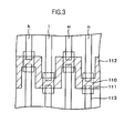
- test TFT 110 is formed for each terminal wiring line 15.
- the test TFT 110 is usually kept turned off.
- the test TFT 110 is turned on by setting a gate electrode 112 to the high level, to detect a short circuit between the terminals 10 and other defects.
- the test TFT 110 includes the gate wiring line (gate electrode) 112, a semiconductor layer 111, which constitutes a channel, and a source/drain electrode 113.
- the SD metal layer 60 extended to the terminal part serves also as the source/drain electrode 113 (SD electrode 113) of the test TFT 110.
- a shared, wide gate electrode 112 runs in the lateral direction across four test TFTs 110.
- the gate electrode 112 is drawn as a wide band in order to avoid complicating the drawing.
- the width of the gate electrode 112 at intersections with the SD metal layer 60 is set small as illustrated in FIG. 3 in order to reduce the capacitance between the gate electrode 112 and the SD electrodes 113.
- FIG. 3 is a schematic plan view in which the overlapping area of the gate wiring line 112 and the SD electrodes 113 in the test TFTs 110 of FIG. 2A is small.
- the terminal part is located above FIG. 3 and the test wiring part is below FIG. 3 .
- the terminal wiring lines k, l, m, and n run from the direction of the terminal part.
- One test TFT 110 is formed for each terminal wiring line.
- Each test TFT 110 is constructed by forming the semiconductor layer (for example, a-Si layer) 111 above the bent gate wiring line 112 with the gate insulating film 55 interposed between the gate wiring line 112 and the semiconductor layer 111, and forming the SD electrode 113 on the semiconductor layer 111.
- the terminal wiring line 15 serves also as the SD electrode 113. As illustrated in FIG. 3 , the gate wiring line 112 is bent to reduce the area of intersections with the SD electrodes 113. The capacitance between the gate wiring line 112 and the SD electrodes 113 is thus made small.
- the test TFTs 110 are formed by the same process that is used to form TFTs within pixels.
- the source/drain electrodes of the test TFTs 110 therefore have to be formed from the SD metal layer 60.
- FIG. 2E which is a sectional view taken along the line D-D of FIG. 2A
- the terminal wiring lines k and m formed from the SD metal layer 60 can be used as the source/drain electrodes 113 of the test TFTs 110 as they are.
- the terminal wiring lines I and n are formed from the gate metal layer 50 and need to switch over to the SD metal layer 60 in order to constitute the source/drain electrodes 113 of the test TFTs 110.
- a terminal for this switchover is the switchover terminal 20.
- the switchover terminal 20 has the same structure as that of the first part 11 of the terminal 10.
- FIG. 2A there is no need to newly form the switchover terminal 20 for the terminal wiring lines k and m, where structures similar to the switchover terminal 20 have been formed in the first part 11 simultaneously.
- only two switchover terminals 20 need to be formed instead of four switchover terminals 20, and hence the longitudinal dimension of FIG. 2A is made smaller by the lengths of two switchover terminals.
- the test wiring line 150 which supplies signals used to check for short circuit and other wiring defects runs in the lateral direction.
- the test wiring line 150 is formed from the gate metal layer 50.
- a structure similar to the first part 11 or the switchover terminal 20 is used for switchover between the test wiring line 150 which is formed from the gate metal layer 50 and the source/drain electrode 113 of the test TFT 110 which is formed from the SD metal layer 60.
- four test wiring lines 150 run in the lateral direction, which means that four systems of wiring lines can be checked for short circuit and other wiring defects.
- FIG. 2B illustrates how the check is conducted.
- short circuit between wiring lines of the same layer is checked between the terminal wiring lines k and m and between the terminal wiring lines I and n
- short circuit between wiring lines of different layers is checked between the terminal wiring lines k and I, between the terminal wiring lines I and m, and between the terminal wiring lines m and n.
- the test wiring line 150 illustrated in FIG. 2A is formed from the gate metal layer 50 and has a constant width in the lateral direction. Similarly to the gate wiring line 120, the test wiring line 150 can be bent in order to reduce the capacitance between the test wiring line 150 and the terminal wiring lines 15 that are formed from the SD metal layer 60, whereby the area of intersections with the terminal wiring lines 15 is made smaller. The capacitance between the test wiring line 150 and the terminal wiring lines 15 can be reduced further if the a-Si layer 111, in addition to the gate insulating film 55, is formed between the test wiring line 150 formed from the gate metal layer 50 and the terminal wiring lines 15 that are formed from the SD metal layer 60.
- test wiring lines 150 are required.
- wiring lines can be laid at a small pitch by bending outward a wiring line on each side of the first part 11 in which the contact holes 41 and 42 are formed.
- This embodiment makes micromachining by light exposure possible even when the terminal pitch x illustrated in FIGS. 2A to 2E is 34 ⁇ m or less. Also, by laying wiring lines in two layers in the terminal part, more tolerance is provided for the reduction in wiring pitch. Further, forming the switchover terminal 20 in the first part 11 makes the region of the switchover terminal 20 for the test TFT 110 smaller, and reduces the size of the display device accordingly.
- FIGS. 4A to 4E illustrate a third embodiment of the present invention.
- FIG. 4A is a plan view. The display area is located above FIG. 4A and an end of the TFT substrate 100 is below FIG. 4A .
- the upper half region TE is the terminal part for connecting with the IC driver 300. Formed below the region TE in FIG. 4A are the region TFT for the test TFT 110 and the region TL for the test wiring line 150.
- This embodiment differs from the second embodiment in that all the terminal wiring lines 15 extended from the display area are formed from the gate metal layer 50. Forming the terminal wiring lines 15 all from the gate metal layer 50 does not hinder micromachining at a small wiring pitch as described in the first embodiment.
- the connection terminals 10 which connect with the bumps 310 of the IC driver 300 each have the first part 11 where the terminal contact hole 41 is formed and the second part 12 where no contact hole is opened and the ITO film 30 alone is formed.
- the first part 11 has, as in the second embodiment, the wiring contact hole 42 for switchover from the gate metal layer 50 to the SD metal layer 60 in addition to the terminal contact hole 41. In this embodiment, every terminal wiring line 15 switches over from the gate metal layer 50 to the SD metal layer 60 in the first part 11 of the terminal 10.
- the test TFT 110 is formed below the region TE in which the terminal part is formed.
- the terminal wiring line 15 needs to be formed from the SD metal layer 60.
- the terminal wiring lines 15 of this embodiment all switch over from the gate metal layer 50 to the SD metal layer 60 in the terminal part, eliminating the need to form the switchover terminals 20 unlike the second embodiment.
- the outside dimensions of the display device can be reduced that much.
- the wide gate electrode 112 runs in the lateral direction to be shared by four test TFTs 110.
- the gate electrode 112 is drawn as a wide band in order to avoid complicating the drawing.
- the width of the gate electrode 112 at intersections with the SD metal layer 60 is set small in order to reduce the capacitance between the gate electrode 112 and the SD electrodes 113, as has been described in the second embodiment with reference to FIG. 3 .
- the test wiring line 150 is formed from the gate metal layer 50 below the test TFTs 110 in FIG. 4A . Two test wiring lines 150 run in this embodiment. All terminal wiring lines can be checked for short circuit with two systems of test wiring lines because the terminal wiring lines of this embodiment are all formed in the same layer, except for the terminal part in which switchover from the gate metal layer 50 to the SD metal layer 60 takes place.
- FIG. 4B is a sectional view taken along the line A-A of FIG. 4A . In this sectional view, all the terminal wiring lines are formed from the gate metal layer 50. FIG. 4B illustrates a sectional view before the terminal wiring line n switches over to the SD metal layer 60 through the ITO film 30 that covers a contact hole formed in the terminal part.
- FIG. 4C is a sectional view taken along the line B-B of FIG. 4A .
- the terminal wiring line n has finished switching over from the gate metal layer 50 to the SD metal layer 60 through the contact holes 41 and 42 and the ITO film 30 that are formed in the terminal part, whereas the terminal wiring line I is switching over through the contact hole 42 formed in the terminal part.
- the terminal wiring lines k and m are still formed from the gate metal layer 50.
- FIG. 4D is a sectional view taken along the line C-C of FIG. 4A .
- the terminal wiring lines I, m, and n have already finished switching over from the gate metal layer 50 to the SD metal layer 60, whereas the terminal wiring line k is switching over from the gate metal layer 50 to the SD metal layer 60 through the terminal contact hole 41 and the ITO film 30 that are formed in the terminal part.
- FIG. 4E is a sectional view taken along the line D-D of FIG. 4A .
- the terminal wiring lines I, m, and n have already finished switching over from the gate metal layer 50 to the SD metal layer 60, whereas the terminal wiring line k has just switched over from the gate metal layer 50 to the SD metal layer 60 through the wiring contact hole 42 and the ITO film 30 that are formed in the terminal part.
- the wiring line interval can be set large by bending the terminal wiring lines 15, and the pitch x between terminals in the lateral direction of FIGS. 4A to 4E can therefore be reduced to 34 ⁇ m or less. Also, switching every terminal wiring line over from the gate metal layer 50 to the SD metal layer 60 in the terminal part eliminates the need to separately form the switchover terminal 20 for connecting the terminal wiring line to the test TFT 110, and is effective to the downsizing of a display device. Further, wiring lines for the terminals 10 of this embodiment are all formed in the same layer, and hence only two systems of the test wiring lines 150 are required, which is advantageous in simplifying the checking step and downsizing a display device. In the case where video signal lines are checked for defects, three systems of the test wiring lines 150 (for example, (one for R signals, one for G signals, and one for B signals) are desirably provided.
- liquid crystal display devices The above-mentioned description is about liquid crystal display devices.
- the present invention can be applied also to other types of display device such as organic EL display devices since the structure of the terminals 10 in other types of display device such as organic EL display devices is basically the same as in liquid crystal display devices.
Landscapes
- Physics & Mathematics (AREA)
- Nonlinear Science (AREA)
- General Physics & Mathematics (AREA)
- Chemical & Material Sciences (AREA)
- Mathematical Physics (AREA)
- Crystallography & Structural Chemistry (AREA)
- Optics & Photonics (AREA)
- Engineering & Computer Science (AREA)
- Theoretical Computer Science (AREA)
- Computer Hardware Design (AREA)
- Liquid Crystal (AREA)
- Devices For Indicating Variable Information By Combining Individual Elements (AREA)
- Vehicle Body Suspensions (AREA)
- Diaphragms For Electromechanical Transducers (AREA)
- Measuring Pulse, Heart Rate, Blood Pressure Or Blood Flow (AREA)
Applications Claiming Priority (1)
| Application Number | Priority Date | Filing Date | Title |
|---|---|---|---|
| JP2007326066A JP4448535B2 (ja) | 2007-12-18 | 2007-12-18 | 表示装置 |
Publications (3)
| Publication Number | Publication Date |
|---|---|
| EP2073054A2 true EP2073054A2 (de) | 2009-06-24 |
| EP2073054A3 EP2073054A3 (de) | 2009-08-12 |
| EP2073054B1 EP2073054B1 (de) | 2010-10-13 |
Family
ID=40457318
Family Applications (1)
| Application Number | Title | Priority Date | Filing Date |
|---|---|---|---|
| EP08171628A Active EP2073054B1 (de) | 2007-12-18 | 2008-12-15 | Anzeigevorrichtung |
Country Status (8)
| Country | Link |
|---|---|
| US (1) | US7924390B2 (de) |
| EP (1) | EP2073054B1 (de) |
| JP (1) | JP4448535B2 (de) |
| KR (1) | KR101021732B1 (de) |
| CN (1) | CN101464574B (de) |
| AT (1) | ATE484768T1 (de) |
| DE (1) | DE602008002990D1 (de) |
| TW (1) | TWI381229B (de) |
Cited By (3)
| Publication number | Priority date | Publication date | Assignee | Title |
|---|---|---|---|---|
| EP2814074A1 (de) * | 2013-05-28 | 2014-12-17 | LG Display Co., Ltd. | Flexible Anzeigevorrichtung und Herstellungsverfahren dafür |
| KR20200007055A (ko) * | 2020-01-08 | 2020-01-21 | 엘지디스플레이 주식회사 | 플렉서블 표시장치 및 그의 제조방법 |
| KR20200145806A (ko) * | 2020-01-08 | 2020-12-30 | 엘지디스플레이 주식회사 | 플렉서블 표시장치 및 그의 제조방법 |
Families Citing this family (23)
| Publication number | Priority date | Publication date | Assignee | Title |
|---|---|---|---|---|
| JP5547427B2 (ja) * | 2009-06-17 | 2014-07-16 | 株式会社ジャパンディスプレイ | 表示装置 |
| US8629965B2 (en) | 2009-06-17 | 2014-01-14 | Hitachi Displays, Ltd. | Display device |
| JP5404289B2 (ja) * | 2009-10-05 | 2014-01-29 | 株式会社ジャパンディスプレイ | 表示パネル |
| JP5431993B2 (ja) * | 2010-02-10 | 2014-03-05 | 株式会社ジャパンディスプレイ | 表示装置 |
| KR101276483B1 (ko) * | 2010-05-13 | 2013-06-18 | 샤프 가부시키가이샤 | 회로 기판 및 표시 장치 |
| JP5730062B2 (ja) | 2011-02-21 | 2015-06-03 | 株式会社ジャパンディスプレイ | 表示装置 |
| JP6022805B2 (ja) | 2012-04-23 | 2016-11-09 | 株式会社ジャパンディスプレイ | 表示装置 |
| US9599866B2 (en) * | 2012-11-08 | 2017-03-21 | Sharp Kabushiki Kaisha | Active matrix substrate and display device |
| US9448454B2 (en) | 2012-11-08 | 2016-09-20 | Sharp Kabushiki Kaisha | Active matrix substrate and display device |
| WO2014073481A1 (ja) * | 2012-11-08 | 2014-05-15 | シャープ株式会社 | アクティブマトリクス基板、及び表示装置 |
| JP6173705B2 (ja) * | 2013-02-07 | 2017-08-02 | 株式会社ジャパンディスプレイ | 表示装置 |
| TWI692280B (zh) * | 2013-03-07 | 2020-04-21 | 日商半導體能源研究所股份有限公司 | 顯示裝置 |
| CN104934440B (zh) * | 2015-04-28 | 2017-12-08 | 京东方科技集团股份有限公司 | 阵列基板及其制作方法、显示装置 |
| CN105974703A (zh) * | 2016-07-13 | 2016-09-28 | 武汉华星光电技术有限公司 | 液晶显示面板 |
| JP2018018006A (ja) * | 2016-07-29 | 2018-02-01 | 株式会社ジャパンディスプレイ | 表示装置 |
| WO2018101159A1 (ja) * | 2016-12-01 | 2018-06-07 | シャープ株式会社 | 接続用配線 |
| KR102593485B1 (ko) * | 2016-12-02 | 2023-10-24 | 삼성디스플레이 주식회사 | 표시 장치 |
| JP6792723B2 (ja) * | 2017-09-26 | 2020-11-25 | シャープ株式会社 | 表示デバイス、表示デバイスの製造方法、表示デバイスの製造装置 |
| JP2020201439A (ja) * | 2019-06-12 | 2020-12-17 | パナソニックIpマネジメント株式会社 | 表示装置 |
| CN211506123U (zh) * | 2019-12-19 | 2020-09-15 | 北京京东方技术开发有限公司 | 一种阵列基板、显示面板及显示装置 |
| CN111402737A (zh) * | 2020-03-26 | 2020-07-10 | 昆山国显光电有限公司 | 一种显示面板 |
| CN113539837B (zh) | 2020-04-17 | 2023-06-23 | 长鑫存储技术有限公司 | 半导体结构引线的制备方法及半导体结构 |
| US12573323B2 (en) * | 2021-06-09 | 2026-03-10 | Sharp Display Technology Corporation | Display device |
Citations (6)
| Publication number | Priority date | Publication date | Assignee | Title |
|---|---|---|---|---|
| US20030040578A1 (en) | 2001-03-27 | 2003-02-27 | Michihiro Sugo | Electrode-forming compositions and electrode members |
| US6590624B1 (en) | 1997-04-11 | 2003-07-08 | Samsung Electronics Co., Ltd. | LCD panels including interconnected test thin film transistors and methods of gross testing LCD panels |
| JP2006181249A (ja) | 2004-12-28 | 2006-07-13 | Yamato Sewing Mach Co Ltd | ミシン |
| JP2006193987A (ja) | 2005-01-14 | 2006-07-27 | Matsushita Electric Works Ltd | 排水管カバー |
| JP2008009246A (ja) | 2006-06-30 | 2008-01-17 | Hitachi Displays Ltd | 表示装置 |
| JP2008020791A (ja) | 2006-07-14 | 2008-01-31 | Hitachi Displays Ltd | 表示装置 |
Family Cites Families (17)
| Publication number | Priority date | Publication date | Assignee | Title |
|---|---|---|---|---|
| EP0845697B1 (de) * | 1995-08-07 | 2004-03-17 | Hitachi, Ltd. | Gegen statische elektrizitat unempfindliche flussigkristall-anzeigevorrichtung mit aktiver matrix |
| TW527513B (en) * | 2000-03-06 | 2003-04-11 | Hitachi Ltd | Liquid crystal display device and manufacturing method thereof |
| KR100390456B1 (ko) * | 2000-12-13 | 2003-07-07 | 엘지.필립스 엘시디 주식회사 | 액정 디스플레이 패널 및 그 제조방법 |
| JP4884586B2 (ja) * | 2000-12-18 | 2012-02-29 | 株式会社 日立ディスプレイズ | 液晶表示装置 |
| KR100737896B1 (ko) * | 2001-02-07 | 2007-07-10 | 삼성전자주식회사 | 어레이 기판과, 액정표시장치 및 그 제조방법 |
| JP2003157020A (ja) * | 2001-11-22 | 2003-05-30 | Advanced Display Inc | フレキシブル基板の実装方法および表示装置 |
| KR100450701B1 (ko) | 2001-12-28 | 2004-10-01 | 엘지.필립스 엘시디 주식회사 | 액정표시장치용 어레이기판과 그 제조방법 |
| JP4006284B2 (ja) | 2002-07-17 | 2007-11-14 | 株式会社 日立ディスプレイズ | 液晶表示装置 |
| TW583446B (en) * | 2003-05-28 | 2004-04-11 | Chunghwa Picture Tubes Ltd | Conducting line structure of a liquid crystal display |
| US7297979B2 (en) | 2003-12-18 | 2007-11-20 | Samsung Electronics Co., Ltd. | Thin film transistor array panel for a display |
| JP2007043049A (ja) * | 2004-12-20 | 2007-02-15 | Matsushita Electric Ind Co Ltd | セル、スタンダードセル、スタンダードセル配置方法、スタンダードセルライブラリ、ならびに半導体集積回路 |
| KR20060078549A (ko) * | 2004-12-31 | 2006-07-05 | 엘지.필립스 엘시디 주식회사 | 액정표시장치 및 그 제조방법 |
| JP2008083072A (ja) * | 2005-01-07 | 2008-04-10 | Sharp Corp | 表示装置 |
| KR101082893B1 (ko) * | 2005-08-24 | 2011-11-11 | 삼성전자주식회사 | 어레이 기판 및 이를 갖는 표시장치 |
| KR20070059668A (ko) * | 2005-12-07 | 2007-06-12 | 엘지.필립스 엘시디 주식회사 | 액정표시장치 |
| JP4783154B2 (ja) * | 2006-01-11 | 2011-09-28 | 東芝モバイルディスプレイ株式会社 | 平面表示装置及びその駆動方法 |
| JP4485559B2 (ja) * | 2007-09-26 | 2010-06-23 | 株式会社 日立ディスプレイズ | 液晶表示装置 |
-
2007
- 2007-12-18 JP JP2007326066A patent/JP4448535B2/ja active Active
-
2008
- 2008-12-02 TW TW097146774A patent/TWI381229B/zh active
- 2008-12-15 AT AT08171628T patent/ATE484768T1/de not_active IP Right Cessation
- 2008-12-15 EP EP08171628A patent/EP2073054B1/de active Active
- 2008-12-15 DE DE602008002990T patent/DE602008002990D1/de active Active
- 2008-12-17 CN CN2008101871502A patent/CN101464574B/zh active Active
- 2008-12-17 US US12/314,843 patent/US7924390B2/en active Active
- 2008-12-17 KR KR1020080128766A patent/KR101021732B1/ko active Active
Patent Citations (6)
| Publication number | Priority date | Publication date | Assignee | Title |
|---|---|---|---|---|
| US6590624B1 (en) | 1997-04-11 | 2003-07-08 | Samsung Electronics Co., Ltd. | LCD panels including interconnected test thin film transistors and methods of gross testing LCD panels |
| US20030040578A1 (en) | 2001-03-27 | 2003-02-27 | Michihiro Sugo | Electrode-forming compositions and electrode members |
| JP2006181249A (ja) | 2004-12-28 | 2006-07-13 | Yamato Sewing Mach Co Ltd | ミシン |
| JP2006193987A (ja) | 2005-01-14 | 2006-07-27 | Matsushita Electric Works Ltd | 排水管カバー |
| JP2008009246A (ja) | 2006-06-30 | 2008-01-17 | Hitachi Displays Ltd | 表示装置 |
| JP2008020791A (ja) | 2006-07-14 | 2008-01-31 | Hitachi Displays Ltd | 表示装置 |
Cited By (7)
| Publication number | Priority date | Publication date | Assignee | Title |
|---|---|---|---|---|
| EP2814074A1 (de) * | 2013-05-28 | 2014-12-17 | LG Display Co., Ltd. | Flexible Anzeigevorrichtung und Herstellungsverfahren dafür |
| US9082667B2 (en) | 2013-05-28 | 2015-07-14 | Lg Display Co., Ltd. | Flexible display device and method for manufacturing the same |
| US9293485B2 (en) | 2013-05-28 | 2016-03-22 | Lg Display Co., Ltd. | Flexible display device and method for manufacturing the same |
| USRE49052E1 (en) | 2013-05-28 | 2022-04-26 | Lg Display Co., Ltd. | Flexible display device and method for manufacturing the same |
| USRE49596E1 (en) | 2013-05-28 | 2023-08-01 | Lg Display Co., Ltd. | Flexible display device and method for manufacturing the same |
| KR20200007055A (ko) * | 2020-01-08 | 2020-01-21 | 엘지디스플레이 주식회사 | 플렉서블 표시장치 및 그의 제조방법 |
| KR20200145806A (ko) * | 2020-01-08 | 2020-12-30 | 엘지디스플레이 주식회사 | 플렉서블 표시장치 및 그의 제조방법 |
Also Published As
| Publication number | Publication date |
|---|---|
| CN101464574B (zh) | 2012-05-30 |
| JP4448535B2 (ja) | 2010-04-14 |
| US20090153008A1 (en) | 2009-06-18 |
| US7924390B2 (en) | 2011-04-12 |
| DE602008002990D1 (de) | 2010-11-25 |
| ATE484768T1 (de) | 2010-10-15 |
| CN101464574A (zh) | 2009-06-24 |
| KR101021732B1 (ko) | 2011-03-15 |
| KR20090066240A (ko) | 2009-06-23 |
| TW200931145A (en) | 2009-07-16 |
| EP2073054A3 (de) | 2009-08-12 |
| EP2073054B1 (de) | 2010-10-13 |
| JP2009145849A (ja) | 2009-07-02 |
| TWI381229B (zh) | 2013-01-01 |
Similar Documents
| Publication | Publication Date | Title |
|---|---|---|
| US7924390B2 (en) | Display device | |
| US11983349B2 (en) | Display device with sensor | |
| US10068545B2 (en) | Display apparatus | |
| CN104380367B (zh) | 显示装置 | |
| US9097920B2 (en) | Display device | |
| CN101950106B (zh) | 显示装置 | |
| KR100763408B1 (ko) | 액정 표시 장치 | |
| JP6681926B2 (ja) | アクティブマトリクス基板及び表示パネル | |
| US9459478B2 (en) | Display apparatus and method of manufacturing the same | |
| US8502950B2 (en) | Substrate for gate-in-panel (GIP) type liquid crystal display device and method for manufacturing the same | |
| JP5431993B2 (ja) | 表示装置 | |
| JP5547427B2 (ja) | 表示装置 | |
| JP2011123162A (ja) | 表示装置 | |
| CN100388100C (zh) | 电光装置、电子设备和安装结构体 | |
| KR20060068442A (ko) | 표시장치용 박막트랜지스터 기판과 그 제조방법 | |
| KR20080052986A (ko) | 액정표시장치와 그 제조방법 | |
| US8169557B2 (en) | Display substrate for liquid crystal display panel | |
| KR100905015B1 (ko) | 끝선이 밝게 빛나는 현상을 제거한 액정표시장치 | |
| US20190079358A1 (en) | Display device | |
| HK1130321B (en) | Display device |
Legal Events
| Date | Code | Title | Description |
|---|---|---|---|
| PUAI | Public reference made under article 153(3) epc to a published international application that has entered the european phase |
Free format text: ORIGINAL CODE: 0009012 |
|
| 17P | Request for examination filed |
Effective date: 20081218 |
|
| AK | Designated contracting states |
Kind code of ref document: A2 Designated state(s): AT BE BG CH CY CZ DE DK EE ES FI FR GB GR HR HU IE IS IT LI LT LU LV MC MT NL NO PL PT RO SE SI SK TR |
|
| AX | Request for extension of the european patent |
Extension state: AL BA MK RS |
|
| PUAL | Search report despatched |
Free format text: ORIGINAL CODE: 0009013 |
|
| AK | Designated contracting states |
Kind code of ref document: A3 Designated state(s): AT BE BG CH CY CZ DE DK EE ES FI FR GB GR HR HU IE IS IT LI LT LU LV MC MT NL NO PL PT RO SE SI SK TR |
|
| AX | Request for extension of the european patent |
Extension state: AL BA MK RS |
|
| RIC1 | Information provided on ipc code assigned before grant |
Ipc: G02F 1/1345 20060101ALN20090709BHEP Ipc: G09G 3/00 20060101ALI20090709BHEP Ipc: G02F 1/13 20060101AFI20090330BHEP |
|
| AKX | Designation fees paid |
Designated state(s): AT BE BG CH CY CZ DE DK EE ES FI FR GB GR HR HU IE IS IT LI LT LU LV MC MT NL NO PL PT RO SE SI SK TR |
|
| GRAP | Despatch of communication of intention to grant a patent |
Free format text: ORIGINAL CODE: EPIDOSNIGR1 |
|
| GRAS | Grant fee paid |
Free format text: ORIGINAL CODE: EPIDOSNIGR3 |
|
| GRAA | (expected) grant |
Free format text: ORIGINAL CODE: 0009210 |
|
| AK | Designated contracting states |
Kind code of ref document: B1 Designated state(s): AT BE BG CH CY CZ DE DK EE ES FI FR GB GR HR HU IE IS IT LI LT LU LV MC MT NL NO PL PT RO SE SI SK TR |
|
| REG | Reference to a national code |
Ref country code: GB Ref legal event code: FG4D |
|
| REG | Reference to a national code |
Ref country code: CH Ref legal event code: EP |
|
| REG | Reference to a national code |
Ref country code: IE Ref legal event code: FG4D |
|
| REF | Corresponds to: |
Ref document number: 602008002990 Country of ref document: DE Date of ref document: 20101125 Kind code of ref document: P |
|
| REG | Reference to a national code |
Ref country code: NL Ref legal event code: VDEP Effective date: 20101013 |
|
| LTIE | Lt: invalidation of european patent or patent extension |
Effective date: 20101013 |
|
| PG25 | Lapsed in a contracting state [announced via postgrant information from national office to epo] |
Ref country code: LT Free format text: LAPSE BECAUSE OF FAILURE TO SUBMIT A TRANSLATION OF THE DESCRIPTION OR TO PAY THE FEE WITHIN THE PRESCRIBED TIME-LIMIT Effective date: 20101013 Ref country code: NO Free format text: LAPSE BECAUSE OF FAILURE TO SUBMIT A TRANSLATION OF THE DESCRIPTION OR TO PAY THE FEE WITHIN THE PRESCRIBED TIME-LIMIT Effective date: 20110113 |
|
| PG25 | Lapsed in a contracting state [announced via postgrant information from national office to epo] |
Ref country code: IS Free format text: LAPSE BECAUSE OF FAILURE TO SUBMIT A TRANSLATION OF THE DESCRIPTION OR TO PAY THE FEE WITHIN THE PRESCRIBED TIME-LIMIT Effective date: 20110213 Ref country code: LV Free format text: LAPSE BECAUSE OF FAILURE TO SUBMIT A TRANSLATION OF THE DESCRIPTION OR TO PAY THE FEE WITHIN THE PRESCRIBED TIME-LIMIT Effective date: 20101013 Ref country code: AT Free format text: LAPSE BECAUSE OF FAILURE TO SUBMIT A TRANSLATION OF THE DESCRIPTION OR TO PAY THE FEE WITHIN THE PRESCRIBED TIME-LIMIT Effective date: 20101013 Ref country code: PT Free format text: LAPSE BECAUSE OF FAILURE TO SUBMIT A TRANSLATION OF THE DESCRIPTION OR TO PAY THE FEE WITHIN THE PRESCRIBED TIME-LIMIT Effective date: 20110214 Ref country code: FI Free format text: LAPSE BECAUSE OF FAILURE TO SUBMIT A TRANSLATION OF THE DESCRIPTION OR TO PAY THE FEE WITHIN THE PRESCRIBED TIME-LIMIT Effective date: 20101013 Ref country code: BG Free format text: LAPSE BECAUSE OF FAILURE TO SUBMIT A TRANSLATION OF THE DESCRIPTION OR TO PAY THE FEE WITHIN THE PRESCRIBED TIME-LIMIT Effective date: 20110113 Ref country code: NL Free format text: LAPSE BECAUSE OF FAILURE TO SUBMIT A TRANSLATION OF THE DESCRIPTION OR TO PAY THE FEE WITHIN THE PRESCRIBED TIME-LIMIT Effective date: 20101013 Ref country code: SE Free format text: LAPSE BECAUSE OF FAILURE TO SUBMIT A TRANSLATION OF THE DESCRIPTION OR TO PAY THE FEE WITHIN THE PRESCRIBED TIME-LIMIT Effective date: 20101013 Ref country code: SI Free format text: LAPSE BECAUSE OF FAILURE TO SUBMIT A TRANSLATION OF THE DESCRIPTION OR TO PAY THE FEE WITHIN THE PRESCRIBED TIME-LIMIT Effective date: 20101013 Ref country code: HR Free format text: LAPSE BECAUSE OF FAILURE TO SUBMIT A TRANSLATION OF THE DESCRIPTION OR TO PAY THE FEE WITHIN THE PRESCRIBED TIME-LIMIT Effective date: 20101013 |
|
| PG25 | Lapsed in a contracting state [announced via postgrant information from national office to epo] |
Ref country code: BE Free format text: LAPSE BECAUSE OF FAILURE TO SUBMIT A TRANSLATION OF THE DESCRIPTION OR TO PAY THE FEE WITHIN THE PRESCRIBED TIME-LIMIT Effective date: 20101013 Ref country code: GR Free format text: LAPSE BECAUSE OF FAILURE TO SUBMIT A TRANSLATION OF THE DESCRIPTION OR TO PAY THE FEE WITHIN THE PRESCRIBED TIME-LIMIT Effective date: 20110114 |
|
| PG25 | Lapsed in a contracting state [announced via postgrant information from national office to epo] |
Ref country code: MC Free format text: LAPSE BECAUSE OF NON-PAYMENT OF DUE FEES Effective date: 20101231 Ref country code: CZ Free format text: LAPSE BECAUSE OF FAILURE TO SUBMIT A TRANSLATION OF THE DESCRIPTION OR TO PAY THE FEE WITHIN THE PRESCRIBED TIME-LIMIT Effective date: 20101013 Ref country code: EE Free format text: LAPSE BECAUSE OF FAILURE TO SUBMIT A TRANSLATION OF THE DESCRIPTION OR TO PAY THE FEE WITHIN THE PRESCRIBED TIME-LIMIT Effective date: 20101013 Ref country code: ES Free format text: LAPSE BECAUSE OF FAILURE TO SUBMIT A TRANSLATION OF THE DESCRIPTION OR TO PAY THE FEE WITHIN THE PRESCRIBED TIME-LIMIT Effective date: 20110124 |
|
| PLBE | No opposition filed within time limit |
Free format text: ORIGINAL CODE: 0009261 |
|
| STAA | Information on the status of an ep patent application or granted ep patent |
Free format text: STATUS: NO OPPOSITION FILED WITHIN TIME LIMIT |
|
| PG25 | Lapsed in a contracting state [announced via postgrant information from national office to epo] |
Ref country code: PL Free format text: LAPSE BECAUSE OF FAILURE TO SUBMIT A TRANSLATION OF THE DESCRIPTION OR TO PAY THE FEE WITHIN THE PRESCRIBED TIME-LIMIT Effective date: 20101013 Ref country code: DK Free format text: LAPSE BECAUSE OF FAILURE TO SUBMIT A TRANSLATION OF THE DESCRIPTION OR TO PAY THE FEE WITHIN THE PRESCRIBED TIME-LIMIT Effective date: 20101013 Ref country code: RO Free format text: LAPSE BECAUSE OF FAILURE TO SUBMIT A TRANSLATION OF THE DESCRIPTION OR TO PAY THE FEE WITHIN THE PRESCRIBED TIME-LIMIT Effective date: 20101013 Ref country code: SK Free format text: LAPSE BECAUSE OF FAILURE TO SUBMIT A TRANSLATION OF THE DESCRIPTION OR TO PAY THE FEE WITHIN THE PRESCRIBED TIME-LIMIT Effective date: 20101013 |
|
| 26N | No opposition filed |
Effective date: 20110714 |
|
| PG25 | Lapsed in a contracting state [announced via postgrant information from national office to epo] |
Ref country code: IE Free format text: LAPSE BECAUSE OF NON-PAYMENT OF DUE FEES Effective date: 20101215 |
|
| REG | Reference to a national code |
Ref country code: DE Ref legal event code: R097 Ref document number: 602008002990 Country of ref document: DE Effective date: 20110714 |
|
| PG25 | Lapsed in a contracting state [announced via postgrant information from national office to epo] |
Ref country code: MT Free format text: LAPSE BECAUSE OF FAILURE TO SUBMIT A TRANSLATION OF THE DESCRIPTION OR TO PAY THE FEE WITHIN THE PRESCRIBED TIME-LIMIT Effective date: 20101013 Ref country code: IT Free format text: LAPSE BECAUSE OF FAILURE TO SUBMIT A TRANSLATION OF THE DESCRIPTION OR TO PAY THE FEE WITHIN THE PRESCRIBED TIME-LIMIT Effective date: 20101013 |
|
| REG | Reference to a national code |
Ref country code: GB Ref legal event code: 732E Free format text: REGISTERED BETWEEN 20120112 AND 20120118 Ref country code: DE Ref legal event code: R082 Ref document number: 602008002990 Country of ref document: DE Representative=s name: PUSCHMANN BORCHERT BARDEHLE PATENTANWAELTE PAR, DE |
|
| REG | Reference to a national code |
Ref country code: GB Ref legal event code: 732E Free format text: REGISTERED BETWEEN 20120119 AND 20120125 |
|
| REG | Reference to a national code |
Ref country code: DE Ref legal event code: R082 Ref document number: 602008002990 Country of ref document: DE Representative=s name: PUSCHMANN BORCHERT BARDEHLE PATENTANWAELTE PAR, DE Effective date: 20120208 Ref country code: DE Ref legal event code: R081 Ref document number: 602008002990 Country of ref document: DE Owner name: PANASONIC LIQUID CRYSTAL DISPLAY CO., LTD., HI, JP Free format text: FORMER OWNER: HITACHI DISPLAYS, LTD., MOBARA, CHIBA, JP Effective date: 20120208 Ref country code: DE Ref legal event code: R081 Ref document number: 602008002990 Country of ref document: DE Owner name: HITACHI DISPLAYS, LTD., MOBARA, JP Free format text: FORMER OWNER: HITACHI DISPLAYS, LTD., MOBARA, CHIBA, JP Effective date: 20120208 Ref country code: DE Ref legal event code: R081 Ref document number: 602008002990 Country of ref document: DE Owner name: HITACHI DISPLAYS, LTD., JP Free format text: FORMER OWNER: HITACHI DISPLAYS, LTD., MOBARA, JP Effective date: 20120208 Ref country code: DE Ref legal event code: R081 Ref document number: 602008002990 Country of ref document: DE Owner name: PANASONIC LIQUID CRYSTAL DISPLAY CO., LTD., JP Free format text: FORMER OWNER: HITACHI DISPLAYS, LTD., MOBARA, JP Effective date: 20120208 |
|
| REG | Reference to a national code |
Ref country code: FR Ref legal event code: TQ Owner name: PANASONIC LIQUID CRYSTAL DISPLAY CO., LTD., JP Effective date: 20120307 Ref country code: FR Ref legal event code: TQ Owner name: HITACHI DISPLAYS, LTD., JP Effective date: 20120307 |
|
| PG25 | Lapsed in a contracting state [announced via postgrant information from national office to epo] |
Ref country code: CY Free format text: LAPSE BECAUSE OF FAILURE TO SUBMIT A TRANSLATION OF THE DESCRIPTION OR TO PAY THE FEE WITHIN THE PRESCRIBED TIME-LIMIT Effective date: 20101013 |
|
| PG25 | Lapsed in a contracting state [announced via postgrant information from national office to epo] |
Ref country code: HU Free format text: LAPSE BECAUSE OF FAILURE TO SUBMIT A TRANSLATION OF THE DESCRIPTION OR TO PAY THE FEE WITHIN THE PRESCRIBED TIME-LIMIT Effective date: 20110414 Ref country code: LU Free format text: LAPSE BECAUSE OF NON-PAYMENT OF DUE FEES Effective date: 20101215 |
|
| PG25 | Lapsed in a contracting state [announced via postgrant information from national office to epo] |
Ref country code: TR Free format text: LAPSE BECAUSE OF FAILURE TO SUBMIT A TRANSLATION OF THE DESCRIPTION OR TO PAY THE FEE WITHIN THE PRESCRIBED TIME-LIMIT Effective date: 20101013 |
|
| REG | Reference to a national code |
Ref country code: CH Ref legal event code: PL |
|
| PG25 | Lapsed in a contracting state [announced via postgrant information from national office to epo] |
Ref country code: LI Free format text: LAPSE BECAUSE OF NON-PAYMENT OF DUE FEES Effective date: 20121231 Ref country code: CH Free format text: LAPSE BECAUSE OF NON-PAYMENT OF DUE FEES Effective date: 20121231 |
|
| REG | Reference to a national code |
Ref country code: FR Ref legal event code: PLFP Year of fee payment: 8 |
|
| REG | Reference to a national code |
Ref country code: FR Ref legal event code: PLFP Year of fee payment: 9 |
|
| REG | Reference to a national code |
Ref country code: FR Ref legal event code: PLFP Year of fee payment: 10 |
|
| REG | Reference to a national code |
Ref country code: DE Ref legal event code: R081 Ref document number: 602008002990 Country of ref document: DE Owner name: PANASONIC INTELLECTUAL PROPERTY CORPORATION OF, US Free format text: FORMER OWNERS: HITACHI DISPLAYS, LTD., MOBARA, CHIBA, JP; PANASONIC LIQUID CRYSTAL DISPLAY CO., LTD., HIMEJI-SHI, HYOGO-KEN, JP Ref country code: DE Ref legal event code: R081 Ref document number: 602008002990 Country of ref document: DE Owner name: JAPAN DISPLAY INC., JP Free format text: FORMER OWNERS: HITACHI DISPLAYS, LTD., MOBARA, CHIBA, JP; PANASONIC LIQUID CRYSTAL DISPLAY CO., LTD., HIMEJI-SHI, HYOGO-KEN, JP Ref country code: DE Ref legal event code: R081 Ref document number: 602008002990 Country of ref document: DE Owner name: MAGNOLIA PURPLE CORP., JP Free format text: FORMER OWNERS: HITACHI DISPLAYS, LTD., MOBARA, CHIBA, JP; PANASONIC LIQUID CRYSTAL DISPLAY CO., LTD., HIMEJI-SHI, HYOGO-KEN, JP |
|
| REG | Reference to a national code |
Ref country code: GB Ref legal event code: 732E Free format text: REGISTERED BETWEEN 20231207 AND 20231213 |
|
| REG | Reference to a national code |
Ref country code: GB Ref legal event code: 732E Free format text: REGISTERED BETWEEN 20250703 AND 20250709 Ref country code: DE Ref legal event code: R081 Ref document number: 602008002990 Country of ref document: DE Owner name: MAGNOLIA PURPLE CORP., JP Free format text: FORMER OWNERS: JAPAN DISPLAY INC., TOKYO, JP; PANASONIC INTELLECTUAL PROPERTY CORPORATION OF AMERICA, TORRANCE, CA, US Ref country code: DE Ref legal event code: R081 Ref document number: 602008002990 Country of ref document: DE Owner name: PANASONIC INTELLECTUAL PROPERTY CORPORATION OF, US Free format text: FORMER OWNERS: JAPAN DISPLAY INC., TOKYO, JP; PANASONIC INTELLECTUAL PROPERTY CORPORATION OF AMERICA, TORRANCE, CA, US |
|
| PGFP | Annual fee paid to national office [announced via postgrant information from national office to epo] |
Ref country code: DE Payment date: 20251028 Year of fee payment: 18 |
|
| PGFP | Annual fee paid to national office [announced via postgrant information from national office to epo] |
Ref country code: GB Payment date: 20251030 Year of fee payment: 18 |
|
| PGFP | Annual fee paid to national office [announced via postgrant information from national office to epo] |
Ref country code: FR Payment date: 20251110 Year of fee payment: 18 |