EP2073094A2 - Temperaturabhängiger Schaltkreis - Google Patents
Temperaturabhängiger Schaltkreis Download PDFInfo
- Publication number
- EP2073094A2 EP2073094A2 EP08167657A EP08167657A EP2073094A2 EP 2073094 A2 EP2073094 A2 EP 2073094A2 EP 08167657 A EP08167657 A EP 08167657A EP 08167657 A EP08167657 A EP 08167657A EP 2073094 A2 EP2073094 A2 EP 2073094A2
- Authority
- EP
- European Patent Office
- Prior art keywords
- temperature
- power
- circuit
- switch
- output
- Prior art date
- Legal status (The legal status is an assumption and is not a legal conclusion. Google has not performed a legal analysis and makes no representation as to the accuracy of the status listed.)
- Granted
Links
Images


Classifications
-
- G—PHYSICS
- G06—COMPUTING OR CALCULATING; COUNTING
- G06F—ELECTRIC DIGITAL DATA PROCESSING
- G06F1/00—Details not covered by groups G06F3/00 - G06F13/00 and G06F21/00
- G06F1/16—Constructional details or arrangements
- G06F1/20—Cooling means
- G06F1/206—Cooling means comprising thermal management
-
- H—ELECTRICITY
- H02—GENERATION; CONVERSION OR DISTRIBUTION OF ELECTRIC POWER
- H02H—EMERGENCY PROTECTIVE CIRCUIT ARRANGEMENTS
- H02H1/00—Details of emergency protective circuit arrangements
- H02H1/06—Arrangements for supplying operative power
-
- H—ELECTRICITY
- H02—GENERATION; CONVERSION OR DISTRIBUTION OF ELECTRIC POWER
- H02H—EMERGENCY PROTECTIVE CIRCUIT ARRANGEMENTS
- H02H5/00—Emergency protective circuit arrangements for automatic disconnection directly responsive to an undesired change from normal non-electric working conditions with or without subsequent reconnection
- H02H5/04—Emergency protective circuit arrangements for automatic disconnection directly responsive to an undesired change from normal non-electric working conditions with or without subsequent reconnection responsive to abnormal temperature
- H02H5/047—Emergency protective circuit arrangements for automatic disconnection directly responsive to an undesired change from normal non-electric working conditions with or without subsequent reconnection responsive to abnormal temperature using a temperature responsive switch
-
- Y—GENERAL TAGGING OF NEW TECHNOLOGICAL DEVELOPMENTS; GENERAL TAGGING OF CROSS-SECTIONAL TECHNOLOGIES SPANNING OVER SEVERAL SECTIONS OF THE IPC; TECHNICAL SUBJECTS COVERED BY FORMER USPC CROSS-REFERENCE ART COLLECTIONS [XRACs] AND DIGESTS
- Y02—TECHNOLOGIES OR APPLICATIONS FOR MITIGATION OR ADAPTATION AGAINST CLIMATE CHANGE
- Y02D—CLIMATE CHANGE MITIGATION TECHNOLOGIES IN INFORMATION AND COMMUNICATION TECHNOLOGIES [ICT], I.E. INFORMATION AND COMMUNICATION TECHNOLOGIES AIMING AT THE REDUCTION OF THEIR OWN ENERGY USE
- Y02D10/00—Energy efficient computing, e.g. low power processors, power management or thermal management
Definitions
- the present invention relates to a circuit for switching off power to electrical equipment if the temperature passes a threshold value.
- a temperature trip switch for shutting down the electrical power to the equipment if the temperature passes a threshold value.
- commercially available temperature switches such as the Maxim MAX6509, may be used to detect an operating temperature and switch an output to trigger an alarm or shut down a sensitive part of the circuitry when a threshold temperature is reached.
- the typical supply current consumed by the MAX6509 temperature switch is around 32 micro amps. In some electrical devices, this is small compared with the normal operating current. However, in battery operated devices, it nevertheless causes an additional drain on the battery. This is particularly an issue for very low power battery operated equipment, as it may significantly shorten the life of the battery.
- the present inventor has addressed such problems of power consumption by a temperature switching device.
- One aspect of the present invention provides a circuit and method for temperature activated switching, by supplying power to a temperature switch only when the temperature approaches a temperature limit at which the temperature switch is operable to switch its output. This reduces the power consumption, because the temperature switch need not be constantly powered up under normal operating conditions.
- the temperature switch has a power input and a switching output for switching at a threshold temperature, and power connection circuitry for connecting or disconnecting power to the power input of the temperature switch.
- An input may be provided for receiving a signal indicating that the current temperature is approaching the threshold temperature of the temperature switch, where the signal is used by the power connection circuitry to control the power supplied to the temperature switch.
- a further input may be provided to indicate that the temperature is no longer approaching the threshold temperature of the temperature switch.
- the temperature switch may be a MAX6509 temperature switch or an alternative equivalent temperature switch or some other type of temperature switch.
- the temperature threshold at which the temperature switch will switch its output may be a fixed value, e.g. set by fixed components in the circuit. Alternatively, it may be a variable value, e.g. influenced by other factors such as the temperature history, the rate of change of temperature, the number of times that the threshold has previously been exceeded, a user adjustable control, etc.
- the circuit may use transistors or logic circuits to control the switching, both for the power output to the temperature sensitive apparatus, and for the power supply to the temperature switch.
- the transistors may comprise FETs or bipolar transistors or a combination of the two
- the logic circuits may comprise arrangements of one or more logic gates, for example, NAND gates, NOR gates, or a combination of the two.
- the electrical equipment being protected preferably includes means for monitoring its own temperature, which may involve continuous temperature measurements, sampled measurements or otherwise. This can be used to generate a signal to initiate the temperature switch being powered up when the threshold temperature is being approached.
- the signal may be a continuous signal, or a single pulse, or some other format of signal such as a series of pulses, indicating that the temperature is within a particular range of the threshold temperature.
- a second signal may be provided to indicate if the temperature has moved sufficiently far away from the threshold temperature to allow the temperature switch to be de-powered again. This second signal may have a similar or different format to the first signal.
- the second signal may be generated at a different temperature from the first signal, e.g. to produce a hysteresis effect in switching on and off of the power to the temperature switch.
- the rate of temperature change as well as the absolute temperature may be a factor in generating the first and/or second signals.
- the circuit is configured for switching on above a temperature threshold, and in other embodiments, the circuit is configured for switching on below a temperature threshold.
- two temperature switches may be used, one switching above a high threshold temperature and the other switching below a low threshold temperature, so that the power sensitive apparatus is only supplied with power between these two thresholds.
- the threshold temperatures for powering up each of the two temperature switches would be selected to leave a normal operating temperature range between them. Then, no more than one of the two temperature switches would be powered up at any given time.
- a user operable switch may be provided for resetting of the temperature trip switch. If the temperature passes the threshold for a first time so that the power is disconnected from the temperature sensitive apparatus, then even if the temperature subsequently passes back through the threshold again, the power may not be automatically restored. A user may activate this switch, e.g. manually or remotely, to once again supply power to the temperature sensitive apparatus. These embodiments are useful for situations where operation should not resume when the temperature returns to an acceptable value. Again, dual temperature switches may be used.
- control lines may be provided to provide signals to the temperature sensitive apparatus indicating that the threshold temperature has been reached.
- the removal of power may be delayed until the temperature sensitive apparatus has completed an operation in progress. Such an operation could be, for example, writing data to a disc drive.
- Embodiments of the invention are particularly useful for battery operated electrical apparatus.
- embodiments of the invention may be used in laptop computers, handheld computers, portable music players, other portable or mobile computing devices, electrical equipment for use in a moving vehicle, mobile or portable communications equipment including radio transceivers and mobile telephones, and any other portable electrical appliances or devices.
- the invention is not limited to battery powered applications, and benefits of the invention may be obtained with any type of electrical apparatus.
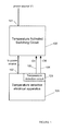
- FIG. 1 shows a temperature sensitive electrical apparatus 120, connected to a temperature activated switching circuit 100.
- the switching circuit 100 is configured for the switching on or off of power to the temperature sensitive electrical apparatus 120, according to a detected temperature.
- the switching circuit 100 is shown as a separate unit to the temperature sensitive apparatus 120, in practice the switching circuit may be provided as a part of the temperature sensitive apparatus rather than a separate unit, and may be located within it.
- the temperature sensitive electrical apparatus 120 has a power input 102, which connects to a power source V1 via the switching circuit 100.
- the input voltage to the temperature sensitive apparatus 120 is V1 when the output of the switching circuit 100 is switched to an "on” setting, and no power is supplied to the temperature sensitive apparatus 120 when the output of the switching circuit 100 is switched to an "off” setting.
- the supplied voltage or current may be reduced when the power switching is operated, or at least some of a plurality of power input connections to the temperature sensitive apparatus 120 may be switched on or off by the switching circuit 100.
- the switching circuit 100 includes a temperature switch, which controls the power output to the temperature sensitive apparatus 120.
- This temperature switch is only supplied with power when the temperature gets close to the switching temperature.
- the temperature switch has its own in-built temperature detector, and a second means of temperature detection is used to control the switching of power to the temperature switch.
- this second means is a temperature detection circuit 121 located within the temperature sensitive apparatus 120.
- both functions may be performed by a single temperature sensor.
- the circuit 121 may include a thermometer, thermostat or other type of temperature sensor, which generates one or more temperature dependent control signals 103, 104, to be fed back to the switching circuit 100 for controlling the power supplied to the temperature switch.
- This temperature sensor may be already present within the temperature sensitive apparatus for some other function, but may be configured for shared use with a circuit according to the present invention.
- the temperature sensor may be configured to detect temperature continuously or discontinuously. It may be configured to measure temperature within a particular temperature range, or to detect when the temperature reaches a particular threshold value.
- the temperature detection circuit 121 may be located within the switching circuit 100, or it may be external to both the switching circuit 100 and the temperature sensitive apparatus 120, e.g. within a power supply for powering the temperature sensitive electrical apparatus 120. However, preferably, it is positioned to be thermally coupled to the temperature sensitive apparatus 120.
- the two temperature dependent control signals 103, 104 are generated by the temperature detection circuit 121, according to the detected temperature.
- the first control signal 103 is generated to indicate when the power should be connected to the temperature switch, and the second control signal 104 is generated to indicate when power should be disconnected from the temperature switch.
- the temperature dependent control signals 103, 104 are received by the switching circuit 100, and are used to control the power supplied to the temperature switch accordingly.
- the temperature switch in the switching circuit 100 is a commercially available temperature switch, such as the Maxim MAX6509.
- the MAX6509 includes a thermostat within its integrated circuit package, for switching its output according to its detected temperature.
- the switching temperature is set by connecting a resistor of selected value to a corresponding control input of the MAX6509 integrated circuit.
- the output of the MAX6509 is used for the switching on or switching off of power to the temperature sensitive electrical apparatus 120.
- the control signals 103, 104 generated by the temperature detection circuit 121 may thus be used to control the connection and disconnection of a voltage to a power input on the MAX6509 integrated circuit.
- the temperature approaches the MAX6509 switching temperature the voltage is applied, thus allowing the MAX6509 to power up and perform its switching function if the switching temperature is reached.
- the voltage is disconnected and no power is supplied to the MAX6509 chip, thus reducing the overall current drain by the power switching circuit 100.
- the power to the temperature switch remains disconnected until the detected temperature approaches its switching threshold.
- the temperature switch thereafter remains powered, regardless of future temperature changes.
- a manually activated reset mechanism may be provided to allow the voltage output to the temperature sensitive apparatus 120 to be turned on, and/or the power to the temperature switch to be turned off once again when the temperature is back to a normal operating range.
- the power to the temperature switch may be disabled as long as the temperature is detected as being outside a critical temperature range, above a selected value, or below a selected value, and only powered on when this condition is not met. The power-on temperature of the temperature switch may be different from the power-off temperature.
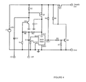
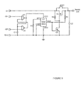
- FIG. 2 shows a circuit according to a first embodiment of the invention.
- the circuit includes a MAX6509 temperature switch, U1.
- the temperature switch U1 has an output -OUT, which is used for controlling the connection of power to the temperature sensitive apparatus.
- a resistor R1 connected between ground and a "SET" input of the temperature switch U1, sets a threshold temperature for the temperature dependent switching of the MAX6509. The output -OUT is not switched until the temperature passes this threshold temperature. At this threshold, the output -OUT is pulled low.
- the temperature switch U1 also includes a hysteresis input "HYST", for selecting the amount of hysteresis in the temperature switching.
- the HYST input is connected to ground, setting the hysteresis to a minimum value (approximately 2°C in the MAX6509).
- a larger amount of hysteresis may be set, if desired, by using a higher voltage on the hysteresis input.
- This temperature switch U1 has a power input VCC, and a ground input GND.
- the circuit shown in Figure 2 is used for disconnecting power from the input VCC of the temperature switch, in order to reduce power consumption by the temperature switch U1 at suitable temperatures.
- either a positive or a negative terminal of the power source, or both may be disconnected from a temperature switch to prevent or reduce the consumption of power at suitable temperatures.
- the circuit of Figure 2 includes a voltage source V1, such as a battery.
- V1 provides 3.6 volts DC, although alternative voltages may be used in other embodiments.
- the negative terminal of the voltage source is connected to ground.
- the positive terminal of the voltage source V1 is connected via a p-channel MOSFET transistor Q1 to a "supply out" power output terminal, which connects to the temperature sensitive electrical apparatus 120 (not shown in figure 2 ) to provide it with power.
- Transistor Q1 is controlled by a second transistor Q4 connected to the output "-OUT" of the temperature switch U1.
- the circuit of Figure 2 has inputs "-On” and “-Off”, which receive the control signals 103, 104 from the temperature detection circuit 121 of the temperature sensitive apparatus 120.
- the minus sign denotes an "active low” on these inputs. This may alternatively be represented by an over-bar or a "_” symbol. Alternatively, the inputs may be simply denoted “On” and “Off”, without indicating an active low. This is particularly useful in embodiments where the inputs are not active low.
- the temperature detection circuit 121 is configured to generate a low voltage pulse on the "-On” input if the temperature reaches a predetermined range of the U1 switching temperature, thus requiring the temperature switch U1 to be powered up.
- the circuit 121 is further configured to generate a low voltage pulse on the "-Off” input if the temperature goes back outside this predetermined temperature range, thus allowing the temperature switch U1 to be de-powered again.
- the form of signals 103 and 104 may be different e.g. high voltages may be used instead of low voltages, and/or continuous signals or some other waveform may be used rather than pulses.
- the "-Off" signal is not implemented, and only the "-On” signal is used.
- the power input VCC of the temperature dependent switch U1 is connected to the positive voltage source V1 via a p-channel MOSFET transistor Q5, so that Q5 can be switched on to power up U1, and switched off to cut the power to U1.
- Capacitor C1 is connected between VCC and ground.
- Resistors R3 and R4 are connected in series between VCC and ground.
- the gate of Q5 is connected to the voltage source V1 via a resistor R2, so that it is initially kept at a high voltage and Q5 is initially switched off.
- the gate of Q5 is also connected via a diode D2 to the "-on"' input.
- the gate of Q5 is also connected to ground via an n-channel MOSFET transistor Q3.
- the gate of Q3 is connected to ground via resistor R4 and to the VCC terminal of U1 via resistor R3. Initially, there is no power connected at VCC, so Q3 is initially kept switched off by R4.
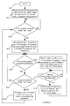
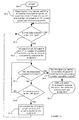
- the flow chart of Figure 3 describes the operation of the circuit of Figure 2 in more detail.
- the process starts at step S1-1.
- power source V1 is connected and no signal is present on the -On and -Off inputs.
- the capacitor C1 is in a discharged state and the transistors Q3 and Q5 are switched off, therefore no power is applied to U1.
- the output (-OUT) of U1 is not pulled low, transistor Q4 is turned on via resistor R5, which turns on transistor Q1 and applies power to the temperature sensitive apparatus 120. which is connected between the supply out and ground pins.
- Resistor R4 (and R3, since C1 is discharged) has the effect of keeping the gate Q3 low and thus keeping it turned off. This keeps Q5 also turned off and thus U1 remains unpowered. This is a stable condition for the circuit.
- the process continues at step S1-3.
- step S1-3 If a pulse is not detected at the -On input, the process remains at step S1-3 until detection of the pulse.
- a low voltage pulse is received at the "-On" terminal, the process continues at step S1-4.
- the voltage at the gate of Q5 is then pulled low by the "-On" pulse, thus switching on transistor Q5.
- the source terminal Q5 is connected to the voltage source V1, and the drain terminal is connected to the VCC power input of U1.
- the effect of Q5 switching on is to provide a voltage V1 at VCC, via Q5, to power up the temperature switch U1.
- Capacitor C1 connected between ground and VCC, stores charge when Q5 is on.
- the resistors R3 and R4 act as a potential divider and supply a suitable voltage to the gate of Q3 to turn it on.
- R3 is significantly lower in value than R4, providing a positive voltage at the gate of Q3.
- the source terminal of Q3 is connected to ground and the drain terminal is connected to the gate of Q5.
- Q3 switched on, a low voltage is supplied via Q3 to the gate of Q5, keeping Q5 switched on.
- the result is that only a single low pulse is required on the -On input to continuously supply power to U1.
- the "-off" terminal is also connected to the gate of transistor Q3 via a diode D1, but no signal is present on the "-off” input at this stage.
- the temperature switch U1 When powered on initially, the temperature switch U1 has its output -OUT switched “off", in a high impedance state.
- the -OUT output is connected to the gate of the n-channel MOSFET transistor Q4, which is also connected to voltage V1 via a resistor R5.
- the gate of Q4 has a high voltage due to R5, and Q4 is accordingly switched on.
- the source and drain terminals of Q4 are connected respectively to ground and to the gate of p-channel MOSFET transistor Q1.
- the gate of Q1 is also connected to V1 via a resistor R6.
- step S1-5 If at step S1-5, the temperature is found to exceed the threshold temperature of U1 set by resistor R1, the process continues to step S1-6, in which the output of the temperature switch -OUT is pulled low. The gate of Q4 is thus pulled low, switching Q4 off. The voltage at the gate of Q1 is then pulled high by R6 connected to V1, so that Q1 is switched off. This has the effect of cutting the power supply to the temperature sensitive apparatus 120. The process then continues to step S1-7.
- step S1-7 if the temperature once more crosses the threshold (plus any hysteresis), so that it is within an acceptable range once again, then the process continues to step S1-8.
- step S1-8 -OUT goes high impedance again, Q4 and Q1 are turned on, power is restored, and the process continues as before at step S1-5.
- step S1-5 If at step S1-5. the temperature has not crossed the threshold, the process goes to step S1-9. At step S1-9, if no signal is detected at the -Off input, then the process goes back to step S1-5. However, if at step S1-9, a low voltage pulse is detected at the -Off input, the process proceeds to step S1-10.
- step S1-10 The low pulse applied to the "'-Off' input causes the gate of transistor Q3 to be pulled low, thus switching off transistor Q3.
- the voltage at the gate of Q5 is then pulled high via R2, so that Q5 switches off.
- the power supply to VCC of U1 is cut off, restoring the circuit to the state in which it started.
- the process moves from step S1-10 back to step S1-3 and continues in this state until a further pulse is received at the -On input.
- Figure 4 shows a further embodiment of the invention, in which bipolar transistors replace the MOSFETs of Figure 1 for Q3 and Q4.
- Three additional resistors are present in the circuit of Figure 4 , to provide suitable biasing to the bipolar transistors. These are R7 connected between the base of Q4 and ground, R8 connected between the base of Q3 and diode D1, and R9 connected between the output of U1 and the base of Q4. Otherwise, the circuit of Figure 4 is the same as that of Figure 2 .
- the circuit of Figure 4 works in the same way as the circuit of Figure 2 .
- FIG. 5 A third embodiment of the invention is shown by the circuit diagram of Figure 5 .
- the circuit of Figure 5 is similar to that of Figure 2 , except for the following differences.
- Figure 5 includes a switch S1 connected, between the source and drain of transistor Q1. Instead of being directly connected to the power source V1; the resistors R2 and R5 and the source terminal of transistor Q5 are connected to V1 via the parallel arrangement of the switch S 1 and the transistor Q1. R6 remains directly connected to V 1.
- a voltage V1 will be supplied at the supply out terminal.
- An additional capacitor C2 is connected between the supply out and ground outputs in the circuit. Otherwise, the circuit of Figure 5 is the same as that of Figure 2 .
- switch S1 is initially in an open position.
- the capacitor C2 remains discharged and hence no power is supplied to the temperature sensitive circuit.
- Resistor R6 holds Q1 turned off, and hence the circuit remains in this state until switch S1 is closed. This powers up the rest of the circuit, which operates as described for Figure 2 and remains powered assuming that the temperature is within the threshold.
- S1 is not held in a closed position, but is opened again after powering the circuit.
- S1 may be biased in the open position so that it will automatically return to an "open" state after being switched to a closed state.
- the -On and -Off inputs are used as described earlier. If, after activating U1 by means of a pulse on the -On input, the temperature crosses the threshold, then Q1 turns off. Since Q1 in Figure 5 also switches off the input voltage to R2, Q5 and R5, then the whole circuit is powered down and remains in this state until S1 is closed again. This embodiment is therefore useful for situations where operation cannot resume when the temperature comes back to an acceptable value.
- FIG. 6 is a flow chart showing the process occurring in the circuit of Figure 5 . This is similar to the process shown in Figure 3 , except that S1 needs to be temporarily closed at step S2-2, and after Q1 is switched off, the circuit remains depowered at step S2-7 until switch S1 is closed again, even if the temperature changes again to an acceptable value.
- two temperature switches may be used instead of one, to set both an upper and lower threshold for the acceptable temperature range.
- Each temperature switch has its own associated circuitry with corresponding transistors Q3 and Q5 etc.
- the -OUT of U1 is open drain in these examples, and thus allows this use of two temperature switches. In normal use, the temperature thresholds would be selected to cause only one at most of the two temperature switches to be powered up at any given time.
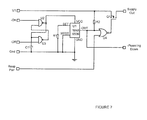
- FIG. 7 shows a circuit according to a fourth embodiment of the invention.
- This circuit uses a logic gate arrangement to perform the switching of power to a MAX6509 temperature switch U1, instead of the Q3/Q5 transistor arrangement of the previous figures.
- the MAX6509 temperature switch has inputs GND, HYST, SET and VCC, and a -OUT output, as discussed with reference to figure 2 .
- the HYST and GND inputs are connected to ground, and the SET input is connected to ground via a resistor R1.
- the circuit of Figure 7 includes an input V1 which is connected to the positive terminal of a voltage source V1.
- the voltage source may be a 3.6V D.C. voltage source as in the earlier figures, or it may have a different voltage.
- the negative terminal of the voltage source is connected to ground.
- the V1 terminal is connected to the positive power connections of the logic gates U2, U3 and U4, and the negative power connections of the logic gates are connected to ground.
- the V1 power terminal is also connected via a p-channel MOSFET transistor Q1 to a "supply out" power output terminal, which connects to the temperature sensitive electrical apparatus 120 (not shown in figure 7 ) to provide it with power.
- Transistor Q1 is controlled by the output of a NOR gate U4, connected to the gate terminal of Q1.
- One input of U4 is connected to the output "-OUT" of the temperature switch U1.
- the other input of this NOR gate is connected to an input terminal labelled "Keep Pwr", which may be driven to a high voltage by the temperature sensitive apparatus to prevent the power being switched off at Q1, or may be tied low if not required.
- the circuit of Figure 7 has inputs "-On” and “-Off, which receive the control signals 103, 104 from the temperature detection circuit 121 of the temperature sensitive apparatus 120, in a similar manner as described with reference to the previous embodiments.
- Both "-On” and “-Off” initially have a high voltage state, but each may be temporarily switched by a low voltage pulse, before returning to a high voltage state once more.
- the "-On” terminal is connected to an input of a first NAND gate U2, and the "-Off” terminal is connected to an input of a second NAND gate U3.
- the NAND gates U2 and U3 are configured as a bistable circuit, with the output of U2 being connected to the second input of U3, and the output of U3 being connected to the second input of U2.
- the power input VCC of the temperature dependent switch U1 is connected to the output of the first NAND gate U2, and a capacitor C1 is also connected between VCC and ground.
- the flow chart of Figure 8 describes the operation of the circuit of Figure 7 in more detail.
- the process starts at step S3-1.
- a power source is connected at the V1 terminal, and a high voltage is present on the -On and -Off inputs.
- the capacitor C1 is in a discharged state and hence one input of the gate U3 is held low. This keeps the output of U3 high, and hence the output of U2 low, since both its outputs are high Therefore, C1 remains discharged, and U3 remains unpowered. This is a stable condition for the circuit.
- the process continues at step S3-3.
- step S3-3 If a low voltage pulse is not detected at the -On input, the process remains at step S3-3 until detection of the pulse.
- step S3-4 One input of the gate U2 is then pulled low by the "-On" pulse, thus switching its output high. This applies power to VCC, charges the capacitor C1 and drives the output of U3 low.
- the output of U3 holds the other input of U2 low, thereby ensuring that the circuit remains in this stable state after completion of the voltage pulse. The result is that only a single low pulse is required on the -On input to continuously supply power to the temperature switch U1.
- the temperature switch U1 When powered on initially, the temperature switch U1 has its output -OUT switched “off", in a high impedance state.
- the -OUT output is connected to one input of a NOR gate U4, and is also connected to voltage V1 via a resistor R2 and to a terminal "-Powering Down", which may be monitored by the temperature sensitive apparatus to allow it to directly detect the state of the temperature switch output.
- the other input to the NOR gate is connected to a terminal "Keep Pwr", which is held low by the temperature sensitive apparatus at this time.
- This output is connected to the gate of p-channel MOSFET transistor Q1.
- the gate of Q1 is pulled low and Q1 is switched on, thus providing a voltage V1 at the "supply out” terminal, to power the temperature sensitive electrical apparatus 120.
- step S3-5 If at step S3-5, the temperature is found to exceed the threshold temperature of U1 set by resistor R1, the process continues to step S3-6, in which the output of the temperature switch -OUT is pulled low, provided that the "Keep Pwr" line is low, as discussed above. The input of U4 is thus pulled low, driving the gate of high, so that Q1 is switched off. This has the effect of cutting the power supply to the temperature sensitive apparatus 120. The process then continues to step S3-7.
- step S3-4 the temperature sensitive apparatus holds the signal "Keep Pwr" high, then the circuit is prevented from turning off the power at Q1, even if the temperature passes the threshold value, because the output of U4 will remain low, keeping Q1 switched on.
- the fact that the circuit is in this state may be determined by the temperature sensitive apparatus monitoring the line "-Powering Down", which is connected to the output of U1. If the output of U1 switches to a low value to indicate that the temperature has passed the threshold, then the temperature sensitive apparatus can complete any necessary operations and then drive the line "Keep Pwr" low. This causes the power to be removed as already described, but having first allowed the necessary operations to be completed, and the process continues to step S3-6 as before. If this functionality is not required, the NOR gate U4 could be replaced by an inverter.
- An alternative use of the "-Powering Down" line is as an interrupt, allowing the temperature sensitive apparatus 120 or some other control circuit to switch off the power at the "supply out” output by supplying a low voltage signal on the "-Powering Down” line, even if the temperature had not passed the threshold value.
- step S3-7 if the temperature once more crosses the threshold (plus any hysteresis), so that it is within an acceptable range once again, then the process continues to step S3-8.
- step S3-8 -OUT goes high impedance again, the output of U4 is driven low and Q1 are turned on, power is restofed, and the process continues as before at step S3-5.
- step S3-8 If the temperature passes back through the threshold before the "Keep Pwr" sign is changed from high to low by the temperature sensitive apparatus, then the process simply continues from step S3-8, and then S3-5, but without any break in the power to the temperature sensitive apparatus having taken place.
- step S3-5 If at step S3-5, the temperature has not crossed the threshold, the process goes to step S3-9. At step S3-9, if no signal is detected at the -Off input, then the process goes back to step S3-5. However, if at step S3-9, a low voltage pulse is detected at the -Off input, the process proceeds to step S3-10.
- FIG. 9 A fifth embodiment of the invention is shown by the circuit diagram of Figure 9 .
- the circuit of Figure 9 is similar to that of Figure 7 , except for the following differences.
- Figure 9 includes a switch S1 connected between the source and drain of transistor Q 1. Instead of being directly connected to the V1 terminal, the resistor R2 and the positive power terminals of U2 and U3 are connected to the supply out terminal of the circuit.
- the gate U4 has been replaced by an N-channel FET Q2 and a resistor R3.
- the "-Powering Down" output and the "Keep Pwr" input are not shown in this embodiment, although they may be included if required.
- An additional capacitor C2 is connected between the supply out and ground outputs in the circuit. Otherwise, the circuit of Figure 9 is the same as that of Figure 7 .
- switch S1 is initially in an open position.
- the capacitor C2 remains discharged and hence no power is supplied to the temperature sensitive circuit.
- Resistor R3 holds Q1 turned off, and hence the circuit remains in this state until switch S1 is closed.
- This powers up the rest of the circuit, which operates as described for Figure 7 and remains powered assuming that the temperature is within the threshold.
- S1 is not held in a closed position, but is opened again after powering the circuit.
- S1 may be biased in the open position so that it will automatically return to an "open" state after being switched to a closed state.
- the -On and -Off inputs are used as described earlier. If, after activating U1by means of a pulse on the -On input, the temperature crosses the threshold, then Q1 turns off. Since Q1 in Figure 9 also switches off the input voltage to U2 and U3, then the whole circuit is powered down and remains in this state until S1 is closed again. This embodiment is therefore useful for situations where operation cannot resume when the temperature comes back to an acceptable value.
- any of the described embodiments it is possible to replace the FETs with bipolar devices, and/or to replace NAND gates with other logic gates or gate arrangements, e.g. NOR gates, or circuits using discrete FETs or bipolar transistors (or a combination of these) having essentially the same functionality.
- FIG 10 is a flow chart showing the process occurring in the circuit of Figure 9 . This is similar to the process shown in Figure 8 , except that S1 needs to be temporarily closed at step S4-2, and after Q1 is switched off, the circuit remains depowered at step S4-7 until switch S1 is closed again, even if the temperature changes again to an acceptable value.
- the temperature switch is only powered up when the temperature approaches the limits. In most cases, this will seldom happen and the temperature switch will mostly remain switched off.
- the current taken when the temperature switch is not powered up is essentially the supply current of U2, U3 and U4, which can be made very low by suitable choice of components. In embodiments with two temperatures switches (one for high temperatures and one for low), at most one of these is powered up at any given time, thereby halving even the maximum current consumption compared with the known prior art.
- the temperature detection circuit or other control circuitry may take other factors into account when making a power switching decision, such as whether the temperature has passed or approached the threshold on a previous occasion, or how quickly the detected temperature is changing. Any combination of such factors may be used to generate a control signal for either switching power to the temperature switch or switching off a voltage to the temperature sensitive apparatus.
Landscapes
- Engineering & Computer Science (AREA)
- Theoretical Computer Science (AREA)
- Human Computer Interaction (AREA)
- Physics & Mathematics (AREA)
- General Engineering & Computer Science (AREA)
- General Physics & Mathematics (AREA)
- Electronic Switches (AREA)
- Control Of Temperature (AREA)
- Power Conversion In General (AREA)
- Dc-Dc Converters (AREA)
Applications Claiming Priority (1)
| Application Number | Priority Date | Filing Date | Title |
|---|---|---|---|
| GB0724803A GB2455750B (en) | 2007-12-19 | 2007-12-19 | Temperature dependent switching circuit |
Publications (3)
| Publication Number | Publication Date |
|---|---|
| EP2073094A2 true EP2073094A2 (de) | 2009-06-24 |
| EP2073094A3 EP2073094A3 (de) | 2011-03-09 |
| EP2073094B1 EP2073094B1 (de) | 2012-04-25 |
Family
ID=39048398
Family Applications (1)
| Application Number | Title | Priority Date | Filing Date |
|---|---|---|---|
| EP20080167657 Not-in-force EP2073094B1 (de) | 2007-12-19 | 2008-10-27 | Temperaturabhängiger Schaltkreis |
Country Status (4)
| Country | Link |
|---|---|
| US (1) | US8212421B2 (de) |
| EP (1) | EP2073094B1 (de) |
| AT (1) | ATE555432T1 (de) |
| GB (1) | GB2455750B (de) |
Families Citing this family (3)
| Publication number | Priority date | Publication date | Assignee | Title |
|---|---|---|---|---|
| US10974606B2 (en) | 2016-08-31 | 2021-04-13 | Cps Technology Holdings Llc | Bi-stable relay |
| DE102021134028A1 (de) * | 2021-12-21 | 2023-06-22 | Infineon Technologies Ag | Thermische regulierung & schutz für leistungselektronische komponenten |
| US12399628B2 (en) * | 2024-01-10 | 2025-08-26 | SK Hynix Inc. | Method and apparatus of performing graceful thermal shutdown in solid state drives |
Family Cites Families (7)
| Publication number | Priority date | Publication date | Assignee | Title |
|---|---|---|---|---|
| US3917970A (en) * | 1974-12-23 | 1975-11-04 | Illinois Tool Works | Temperature sensor with hysteresis |
| FR2348832A1 (fr) * | 1976-04-20 | 1977-11-18 | Ferodo Sa | Perfectionnements aux circuits d'alimentation de moteurs electriques,notamment d'un moto-ventilateur de refroidissement d'un radiateur de vehicule automobile |
| US5881298A (en) * | 1996-09-05 | 1999-03-09 | Micron Technology, Inc. | Portable computer with selectively operable cooling unit |
| US5835885A (en) * | 1997-06-05 | 1998-11-10 | Giga-Byte Technology Co., Ltd. | Over temperature protection method and device for a central processing unit |
| JP2003088100A (ja) * | 2001-09-13 | 2003-03-20 | Tdk Corp | スイッチング電源装置 |
| JP4039163B2 (ja) * | 2002-08-01 | 2008-01-30 | ソニー株式会社 | マルチチップモジュール、マルチチップモジュールのシャットダウン方法 |
| US6935130B2 (en) * | 2003-06-24 | 2005-08-30 | Aopen Inc. | Computer cooling system |
-
2007
- 2007-12-19 GB GB0724803A patent/GB2455750B/en not_active Expired - Fee Related
-
2008
- 2008-10-27 EP EP20080167657 patent/EP2073094B1/de not_active Not-in-force
- 2008-10-27 AT AT08167657T patent/ATE555432T1/de active
- 2008-12-03 US US12/327,106 patent/US8212421B2/en not_active Expired - Fee Related
Also Published As
| Publication number | Publication date |
|---|---|
| GB2455750A (en) | 2009-06-24 |
| EP2073094B1 (de) | 2012-04-25 |
| GB2455750B (en) | 2012-06-13 |
| US8212421B2 (en) | 2012-07-03 |
| EP2073094A3 (de) | 2011-03-09 |
| US20090315665A1 (en) | 2009-12-24 |
| GB0724803D0 (en) | 2008-01-30 |
| ATE555432T1 (de) | 2012-05-15 |
Similar Documents
| Publication | Publication Date | Title |
|---|---|---|
| US20110163723A1 (en) | Battery pack and method of battery pack power management | |
| US7679224B2 (en) | Circuit for protecting computer | |
| JP5608544B2 (ja) | 出力回路 | |
| KR960024821A (ko) | 전원관리기구, 전원관리방법, 및 입출력장치용 제어기 | |
| US10530356B2 (en) | Overcurrent detection circuit and method, load switch, and portable device | |
| CN110726938B (zh) | 电流感测系统及其实现方法和集成电路 | |
| CN101183795A (zh) | 在电池组的备用状态期间具有低功耗的电池状态监测电路 | |
| CN101604867A (zh) | 一种主电源与后备电源的切换方法和切换电路 | |
| WO2002008874A3 (en) | Method and apparatus to provide deterministic power-on voltage in a system having processor-controlled voltage level | |
| US7383449B2 (en) | Power management for connected circuits | |
| JP2011514581A5 (de) | ||
| EP2073094B1 (de) | Temperaturabhängiger Schaltkreis | |
| US8308316B2 (en) | Lamp | |
| CN103959648A (zh) | 节约电荷的功率门控装置和方法 | |
| US8754551B2 (en) | Electric power supply control circuit | |
| JP3853759B2 (ja) | 移動携帯端末 | |
| CN216649230U (zh) | 一种低功耗高温保护电路 | |
| JP2002171749A (ja) | 過電流保護機能を有するスイッチングレギュレータおよびそれを用いた電子機器 | |
| JP2007222000A (ja) | 過電流保護機能を有するスイッチングレギュレータおよびそれを用いた電子機器 | |
| KR100534110B1 (ko) | Usb전원공급장치 | |
| CN102799249B (zh) | 一种计算机及其电源控制装置 | |
| US9935431B2 (en) | Power supply identification apparatus and power supply identification method | |
| KR20120092919A (ko) | Atx 시스템의 온/오프 기능을 제어하기 위한 장치 | |
| US8988134B2 (en) | System and method for operating low power circuits at high temperatures | |
| KR100662435B1 (ko) | 발열방지를 위한 충전회로 |
Legal Events
| Date | Code | Title | Description |
|---|---|---|---|
| PUAI | Public reference made under article 153(3) epc to a published international application that has entered the european phase |
Free format text: ORIGINAL CODE: 0009012 |
|
| AK | Designated contracting states |
Kind code of ref document: A2 Designated state(s): AT BE BG CH CY CZ DE DK EE ES FI FR GB GR HR HU IE IS IT LI LT LU LV MC MT NL NO PL PT RO SE SI SK TR |
|
| AX | Request for extension of the european patent |
Extension state: AL BA MK RS |
|
| PUAL | Search report despatched |
Free format text: ORIGINAL CODE: 0009013 |
|
| AK | Designated contracting states |
Kind code of ref document: A3 Designated state(s): AT BE BG CH CY CZ DE DK EE ES FI FR GB GR HR HU IE IS IT LI LT LU LV MC MT NL NO PL PT RO SE SI SK TR |
|
| AX | Request for extension of the european patent |
Extension state: AL BA MK RS |
|
| 17P | Request for examination filed |
Effective date: 20110412 |
|
| AKX | Designation fees paid |
Designated state(s): AT BE BG CH CY CZ DE DK EE ES FI FR GB GR HR HU IE IS IT LI LT LU LV MC MT NL NO PL PT RO SE SI SK TR |
|
| GRAP | Despatch of communication of intention to grant a patent |
Free format text: ORIGINAL CODE: EPIDOSNIGR1 |
|
| RTI1 | Title (correction) |
Free format text: TEMPERATURE DEPENDENT SWITCHING CIRCUIT |
|
| GRAS | Grant fee paid |
Free format text: ORIGINAL CODE: EPIDOSNIGR3 |
|
| GRAA | (expected) grant |
Free format text: ORIGINAL CODE: 0009210 |
|
| AK | Designated contracting states |
Kind code of ref document: B1 Designated state(s): AT BE BG CH CY CZ DE DK EE ES FI FR GB GR HR HU IE IS IT LI LT LU LV MC MT NL NO PL PT RO SE SI SK TR |
|
| REG | Reference to a national code |
Ref country code: GB Ref legal event code: FG4D |
|
| REG | Reference to a national code |
Ref country code: CH Ref legal event code: EP |
|
| REG | Reference to a national code |
Ref country code: AT Ref legal event code: REF Ref document number: 555432 Country of ref document: AT Kind code of ref document: T Effective date: 20120515 |
|
| REG | Reference to a national code |
Ref country code: IE Ref legal event code: FG4D |
|
| REG | Reference to a national code |
Ref country code: DE Ref legal event code: R096 Ref document number: 602008015148 Country of ref document: DE Effective date: 20120628 |
|
| REG | Reference to a national code |
Ref country code: NL Ref legal event code: VDEP Effective date: 20120425 |
|
| REG | Reference to a national code |
Ref country code: AT Ref legal event code: MK05 Ref document number: 555432 Country of ref document: AT Kind code of ref document: T Effective date: 20120425 |
|
| LTIE | Lt: invalidation of european patent or patent extension |
Effective date: 20120425 |
|
| PG25 | Lapsed in a contracting state [announced via postgrant information from national office to epo] |
Ref country code: CY Free format text: LAPSE BECAUSE OF FAILURE TO SUBMIT A TRANSLATION OF THE DESCRIPTION OR TO PAY THE FEE WITHIN THE PRESCRIBED TIME-LIMIT Effective date: 20120425 Ref country code: PL Free format text: LAPSE BECAUSE OF FAILURE TO SUBMIT A TRANSLATION OF THE DESCRIPTION OR TO PAY THE FEE WITHIN THE PRESCRIBED TIME-LIMIT Effective date: 20120425 Ref country code: FI Free format text: LAPSE BECAUSE OF FAILURE TO SUBMIT A TRANSLATION OF THE DESCRIPTION OR TO PAY THE FEE WITHIN THE PRESCRIBED TIME-LIMIT Effective date: 20120425 Ref country code: IS Free format text: LAPSE BECAUSE OF FAILURE TO SUBMIT A TRANSLATION OF THE DESCRIPTION OR TO PAY THE FEE WITHIN THE PRESCRIBED TIME-LIMIT Effective date: 20120825 Ref country code: LT Free format text: LAPSE BECAUSE OF FAILURE TO SUBMIT A TRANSLATION OF THE DESCRIPTION OR TO PAY THE FEE WITHIN THE PRESCRIBED TIME-LIMIT Effective date: 20120425 Ref country code: SE Free format text: LAPSE BECAUSE OF FAILURE TO SUBMIT A TRANSLATION OF THE DESCRIPTION OR TO PAY THE FEE WITHIN THE PRESCRIBED TIME-LIMIT Effective date: 20120425 Ref country code: NO Free format text: LAPSE BECAUSE OF FAILURE TO SUBMIT A TRANSLATION OF THE DESCRIPTION OR TO PAY THE FEE WITHIN THE PRESCRIBED TIME-LIMIT Effective date: 20120725 |
|
| PG25 | Lapsed in a contracting state [announced via postgrant information from national office to epo] |
Ref country code: PT Free format text: LAPSE BECAUSE OF FAILURE TO SUBMIT A TRANSLATION OF THE DESCRIPTION OR TO PAY THE FEE WITHIN THE PRESCRIBED TIME-LIMIT Effective date: 20120827 Ref country code: HR Free format text: LAPSE BECAUSE OF FAILURE TO SUBMIT A TRANSLATION OF THE DESCRIPTION OR TO PAY THE FEE WITHIN THE PRESCRIBED TIME-LIMIT Effective date: 20120425 Ref country code: LV Free format text: LAPSE BECAUSE OF FAILURE TO SUBMIT A TRANSLATION OF THE DESCRIPTION OR TO PAY THE FEE WITHIN THE PRESCRIBED TIME-LIMIT Effective date: 20120425 Ref country code: GR Free format text: LAPSE BECAUSE OF FAILURE TO SUBMIT A TRANSLATION OF THE DESCRIPTION OR TO PAY THE FEE WITHIN THE PRESCRIBED TIME-LIMIT Effective date: 20120726 Ref country code: SI Free format text: LAPSE BECAUSE OF FAILURE TO SUBMIT A TRANSLATION OF THE DESCRIPTION OR TO PAY THE FEE WITHIN THE PRESCRIBED TIME-LIMIT Effective date: 20120425 |
|
| PG25 | Lapsed in a contracting state [announced via postgrant information from national office to epo] |
Ref country code: BE Free format text: LAPSE BECAUSE OF FAILURE TO SUBMIT A TRANSLATION OF THE DESCRIPTION OR TO PAY THE FEE WITHIN THE PRESCRIBED TIME-LIMIT Effective date: 20120425 |
|
| PG25 | Lapsed in a contracting state [announced via postgrant information from national office to epo] |
Ref country code: SK Free format text: LAPSE BECAUSE OF FAILURE TO SUBMIT A TRANSLATION OF THE DESCRIPTION OR TO PAY THE FEE WITHIN THE PRESCRIBED TIME-LIMIT Effective date: 20120425 Ref country code: DK Free format text: LAPSE BECAUSE OF FAILURE TO SUBMIT A TRANSLATION OF THE DESCRIPTION OR TO PAY THE FEE WITHIN THE PRESCRIBED TIME-LIMIT Effective date: 20120425 Ref country code: RO Free format text: LAPSE BECAUSE OF FAILURE TO SUBMIT A TRANSLATION OF THE DESCRIPTION OR TO PAY THE FEE WITHIN THE PRESCRIBED TIME-LIMIT Effective date: 20120425 Ref country code: EE Free format text: LAPSE BECAUSE OF FAILURE TO SUBMIT A TRANSLATION OF THE DESCRIPTION OR TO PAY THE FEE WITHIN THE PRESCRIBED TIME-LIMIT Effective date: 20120425 Ref country code: AT Free format text: LAPSE BECAUSE OF FAILURE TO SUBMIT A TRANSLATION OF THE DESCRIPTION OR TO PAY THE FEE WITHIN THE PRESCRIBED TIME-LIMIT Effective date: 20120425 Ref country code: CZ Free format text: LAPSE BECAUSE OF FAILURE TO SUBMIT A TRANSLATION OF THE DESCRIPTION OR TO PAY THE FEE WITHIN THE PRESCRIBED TIME-LIMIT Effective date: 20120425 Ref country code: NL Free format text: LAPSE BECAUSE OF FAILURE TO SUBMIT A TRANSLATION OF THE DESCRIPTION OR TO PAY THE FEE WITHIN THE PRESCRIBED TIME-LIMIT Effective date: 20120425 |
|
| PG25 | Lapsed in a contracting state [announced via postgrant information from national office to epo] |
Ref country code: IT Free format text: LAPSE BECAUSE OF FAILURE TO SUBMIT A TRANSLATION OF THE DESCRIPTION OR TO PAY THE FEE WITHIN THE PRESCRIBED TIME-LIMIT Effective date: 20120425 |
|
| PLBE | No opposition filed within time limit |
Free format text: ORIGINAL CODE: 0009261 |
|
| STAA | Information on the status of an ep patent application or granted ep patent |
Free format text: STATUS: NO OPPOSITION FILED WITHIN TIME LIMIT |
|
| 26N | No opposition filed |
Effective date: 20130128 |
|
| PG25 | Lapsed in a contracting state [announced via postgrant information from national office to epo] |
Ref country code: ES Free format text: LAPSE BECAUSE OF FAILURE TO SUBMIT A TRANSLATION OF THE DESCRIPTION OR TO PAY THE FEE WITHIN THE PRESCRIBED TIME-LIMIT Effective date: 20120805 |
|
| REG | Reference to a national code |
Ref country code: DE Ref legal event code: R097 Ref document number: 602008015148 Country of ref document: DE Effective date: 20130128 |
|
| PG25 | Lapsed in a contracting state [announced via postgrant information from national office to epo] |
Ref country code: MC Free format text: LAPSE BECAUSE OF NON-PAYMENT OF DUE FEES Effective date: 20121031 |
|
| REG | Reference to a national code |
Ref country code: CH Ref legal event code: PL |
|
| PG25 | Lapsed in a contracting state [announced via postgrant information from national office to epo] |
Ref country code: LI Free format text: LAPSE BECAUSE OF NON-PAYMENT OF DUE FEES Effective date: 20121031 Ref country code: BG Free format text: LAPSE BECAUSE OF FAILURE TO SUBMIT A TRANSLATION OF THE DESCRIPTION OR TO PAY THE FEE WITHIN THE PRESCRIBED TIME-LIMIT Effective date: 20120725 Ref country code: CH Free format text: LAPSE BECAUSE OF NON-PAYMENT OF DUE FEES Effective date: 20121031 |
|
| REG | Reference to a national code |
Ref country code: IE Ref legal event code: MM4A |
|
| PG25 | Lapsed in a contracting state [announced via postgrant information from national office to epo] |
Ref country code: IE Free format text: LAPSE BECAUSE OF NON-PAYMENT OF DUE FEES Effective date: 20121027 |
|
| PG25 | Lapsed in a contracting state [announced via postgrant information from national office to epo] |
Ref country code: MT Free format text: LAPSE BECAUSE OF FAILURE TO SUBMIT A TRANSLATION OF THE DESCRIPTION OR TO PAY THE FEE WITHIN THE PRESCRIBED TIME-LIMIT Effective date: 20120425 |
|
| PG25 | Lapsed in a contracting state [announced via postgrant information from national office to epo] |
Ref country code: TR Free format text: LAPSE BECAUSE OF FAILURE TO SUBMIT A TRANSLATION OF THE DESCRIPTION OR TO PAY THE FEE WITHIN THE PRESCRIBED TIME-LIMIT Effective date: 20120425 |
|
| PG25 | Lapsed in a contracting state [announced via postgrant information from national office to epo] |
Ref country code: LU Free format text: LAPSE BECAUSE OF NON-PAYMENT OF DUE FEES Effective date: 20121027 |
|
| PG25 | Lapsed in a contracting state [announced via postgrant information from national office to epo] |
Ref country code: HU Free format text: LAPSE BECAUSE OF FAILURE TO SUBMIT A TRANSLATION OF THE DESCRIPTION OR TO PAY THE FEE WITHIN THE PRESCRIBED TIME-LIMIT Effective date: 20081027 |
|
| REG | Reference to a national code |
Ref country code: FR Ref legal event code: PLFP Year of fee payment: 8 |
|
| PGFP | Annual fee paid to national office [announced via postgrant information from national office to epo] |
Ref country code: FR Payment date: 20150923 Year of fee payment: 8 |
|
| PGFP | Annual fee paid to national office [announced via postgrant information from national office to epo] |
Ref country code: GB Payment date: 20151021 Year of fee payment: 8 Ref country code: DE Payment date: 20151020 Year of fee payment: 8 |
|
| REG | Reference to a national code |
Ref country code: DE Ref legal event code: R119 Ref document number: 602008015148 Country of ref document: DE |
|
| GBPC | Gb: european patent ceased through non-payment of renewal fee |
Effective date: 20161027 |
|
| REG | Reference to a national code |
Ref country code: FR Ref legal event code: ST Effective date: 20170630 |
|
| PG25 | Lapsed in a contracting state [announced via postgrant information from national office to epo] |
Ref country code: FR Free format text: LAPSE BECAUSE OF NON-PAYMENT OF DUE FEES Effective date: 20161102 Ref country code: GB Free format text: LAPSE BECAUSE OF NON-PAYMENT OF DUE FEES Effective date: 20161027 Ref country code: DE Free format text: LAPSE BECAUSE OF NON-PAYMENT OF DUE FEES Effective date: 20170503 |
|
| P01 | Opt-out of the competence of the unified patent court (upc) registered |
Effective date: 20230512 |