EP2073154A1 - Biometrisches Mikromodul - Google Patents
Biometrisches Mikromodul Download PDFInfo
- Publication number
- EP2073154A1 EP2073154A1 EP07291576A EP07291576A EP2073154A1 EP 2073154 A1 EP2073154 A1 EP 2073154A1 EP 07291576 A EP07291576 A EP 07291576A EP 07291576 A EP07291576 A EP 07291576A EP 2073154 A1 EP2073154 A1 EP 2073154A1
- Authority
- EP
- European Patent Office
- Prior art keywords
- micro
- module
- card
- contact
- electrical contacts
- Prior art date
- Legal status (The legal status is an assumption and is not a legal conclusion. Google has not performed a legal analysis and makes no representation as to the accuracy of the status listed.)
- Withdrawn
Links
Images

Classifications
-
- G—PHYSICS
- G06—COMPUTING OR CALCULATING; COUNTING
- G06K—GRAPHICAL DATA READING; PRESENTATION OF DATA; RECORD CARRIERS; HANDLING RECORD CARRIERS
- G06K19/00—Record carriers for use with machines and with at least a part designed to carry digital markings
- G06K19/06—Record carriers for use with machines and with at least a part designed to carry digital markings characterised by the kind of the digital marking, e.g. shape, nature, code
- G06K19/067—Record carriers with conductive marks, printed circuits or semiconductor circuit elements, e.g. credit or identity cards also with resonating or responding marks without active components
- G06K19/07—Record carriers with conductive marks, printed circuits or semiconductor circuit elements, e.g. credit or identity cards also with resonating or responding marks without active components with integrated circuit chips
- G06K19/077—Constructional details, e.g. mounting of circuits in the carrier
- G06K19/07745—Mounting details of integrated circuit chips
-
- G—PHYSICS
- G06—COMPUTING OR CALCULATING; COUNTING
- G06K—GRAPHICAL DATA READING; PRESENTATION OF DATA; RECORD CARRIERS; HANDLING RECORD CARRIERS
- G06K19/00—Record carriers for use with machines and with at least a part designed to carry digital markings
- G06K19/06—Record carriers for use with machines and with at least a part designed to carry digital markings characterised by the kind of the digital marking, e.g. shape, nature, code
- G06K19/067—Record carriers with conductive marks, printed circuits or semiconductor circuit elements, e.g. credit or identity cards also with resonating or responding marks without active components
- G06K19/07—Record carriers with conductive marks, printed circuits or semiconductor circuit elements, e.g. credit or identity cards also with resonating or responding marks without active components with integrated circuit chips
- G06K19/0716—Record carriers with conductive marks, printed circuits or semiconductor circuit elements, e.g. credit or identity cards also with resonating or responding marks without active components with integrated circuit chips at least one of the integrated circuit chips comprising a sensor or an interface to a sensor
- G06K19/0718—Record carriers with conductive marks, printed circuits or semiconductor circuit elements, e.g. credit or identity cards also with resonating or responding marks without active components with integrated circuit chips at least one of the integrated circuit chips comprising a sensor or an interface to a sensor the sensor being of the biometric kind, e.g. fingerprint sensors
-
- G—PHYSICS
- G06—COMPUTING OR CALCULATING; COUNTING
- G06K—GRAPHICAL DATA READING; PRESENTATION OF DATA; RECORD CARRIERS; HANDLING RECORD CARRIERS
- G06K19/00—Record carriers for use with machines and with at least a part designed to carry digital markings
- G06K19/06—Record carriers for use with machines and with at least a part designed to carry digital markings characterised by the kind of the digital marking, e.g. shape, nature, code
- G06K19/067—Record carriers with conductive marks, printed circuits or semiconductor circuit elements, e.g. credit or identity cards also with resonating or responding marks without active components
- G06K19/07—Record carriers with conductive marks, printed circuits or semiconductor circuit elements, e.g. credit or identity cards also with resonating or responding marks without active components with integrated circuit chips
- G06K19/077—Constructional details, e.g. mounting of circuits in the carrier
- G06K19/07745—Mounting details of integrated circuit chips
- G06K19/07747—Mounting details of integrated circuit chips at least one of the integrated circuit chips being mounted as a module
-
- G—PHYSICS
- G06—COMPUTING OR CALCULATING; COUNTING
- G06K—GRAPHICAL DATA READING; PRESENTATION OF DATA; RECORD CARRIERS; HANDLING RECORD CARRIERS
- G06K19/00—Record carriers for use with machines and with at least a part designed to carry digital markings
- G06K19/06—Record carriers for use with machines and with at least a part designed to carry digital markings characterised by the kind of the digital marking, e.g. shape, nature, code
- G06K19/067—Record carriers with conductive marks, printed circuits or semiconductor circuit elements, e.g. credit or identity cards also with resonating or responding marks without active components
- G06K19/07—Record carriers with conductive marks, printed circuits or semiconductor circuit elements, e.g. credit or identity cards also with resonating or responding marks without active components with integrated circuit chips
- G06K19/077—Constructional details, e.g. mounting of circuits in the carrier
- G06K19/07749—Constructional details, e.g. mounting of circuits in the carrier the record carrier being capable of non-contact communication, e.g. constructional details of the antenna of a non-contact smart card
- G06K19/07766—Constructional details, e.g. mounting of circuits in the carrier the record carrier being capable of non-contact communication, e.g. constructional details of the antenna of a non-contact smart card comprising at least a second communication arrangement in addition to a first non-contact communication arrangement
- G06K19/07769—Constructional details, e.g. mounting of circuits in the carrier the record carrier being capable of non-contact communication, e.g. constructional details of the antenna of a non-contact smart card comprising at least a second communication arrangement in addition to a first non-contact communication arrangement the further communication means being a galvanic interface, e.g. hybrid or mixed smart cards having a contact and a non-contact interface
Definitions
- the invention relates to micro-modules, in particular micro-modules used for smart cards.
- a smart card, chip card, or integrated circuit card can be any pocket-sized card with one or more embedded integrated circuit.
- Smart cards can typically receive input, process the input, and deliver an output.
- Smart cards may be simple memory cards containing only non-volatile memory storage components, and possibly some specific security logic. But smart cards can also be more elaborate microprocessor cards containing volatile memory and microprocessor components.
- Smart cards bodies are typically made of plastic, generally PVC or ABS. Smart cards dimensions typically correspond to credit card size.
- the ID-1 form factor of ISO 7810 defines 85.60 x 53.98 mm smart cards.
- Another popular size is ID-000 which is 25 x 15 mm. Both are .76 mm thick.
- Smart cards can comprise a contact interface (for example as specified in ISO 7816-2), a contact-less interface (such as Mifare), or both (combicards). When multiple interfaces are provided, each interface may be associated with a specific chip, or a single chip may be provided with multiple interfaces.
- Contact smart cards typically comprise a micro-module which outside surface (i.e. the surface of the micro-module which is visible once the micro-module has been embedded in the smart card) is in general rectangular (about 1cm by 1cm) and mostly metallic (e.g. gold) since it consists primarily of electrical contacts. When the smart card is inserted into a reader, the outside surface of the micro-module establishes contact with corresponding electrical connectors of the reader.
- the reader can then read information from the smart card, write information back, etc.
- ISO/IEC 7816 and ISO/IEC 7810 series of standards define possible physical shape and positions of the electrical connectors, the electrical characteristics, the communications protocols, the format of the commands sent to the smart card and the responses returned by the smart card, robustness of the card, the functionality.
- Contact smart cards may contain batteries, but most often energy is supplied by the smart card reader.
- a second type is the contactless smart card, in which the chip communicates with the card reader for example through RFID induction technology (typically at data rates of 106 to 848 kbit/s). These cards require proximity to an antenna to complete transaction.
- a standard for contact-less smart card communications is ISO/IEC 14443, dated 2001. It defines two types of contact-less cards ("A" and "B"), and allows for communications at distances up to 10 cm. There had been proposals for ISO 14443 types C, D, E and F that have been rejected by the International Organization for Standardization. An alternative standard for contact-less smart cards is ISO 15693, which allows communications at distances up to 50 cm.
- Examples of payment cards which are adapted for contact-less technology comprise products from Visa (Quick VSDC - "qVSDC", Visa Wave, MSD), MasterCard (PayPass Magstripe, PayPass MChip), or American Express (Express Pay).
- Major roll-outs of contact-less payment cards started in 2005 in USA, and in 2006 in Asia and Europe. Contact-less transactions typically cover a payment range of ⁇ $5-50 only because the user does not type a PIN code.
- Non-EMV cards typically work like magnetic stripe cards, which is a typical card technology in the USA (see PayPass Magstripe and VISA MSD). Such cards typically do not control the remaining amount.
- EMV cards may have two interfaces (contact and contact-less) and may work as a normal EMV card via contact interface. Via contact-less interface they work almost like an EMV (card command sequence adopted on contact-less features as low power and short transaction time).
- micro-module which is usable in particular to manufacture more easily a smart card with finger print recognition capability.
- the micro-module according the invention is also suitable to manufacture other types of devices, such as MMC or SD cards, or any device comprising a contact interface with an internal chip.
- Figure 1 represents a known method for embedding a micro module on a smart card
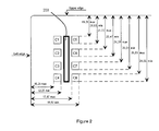
- Figure 2 represents a smart card comprising a micro-module according to a preferred embodiment of the invention.
- Figure 1 shows a simplified process for creating a basic micro-module according to state of the art and embedding it in a known smart card body.
- a chip 100 is transferred onto a continuous metal strip 102.
- the metal strip contains electrical contacts which are connected to corresponding contacts on the chip (e.g. gold wire bonding).
- An electrical contact should be understood according to the definition given for example in ISO 7816-1, that is: a conducting element ensuring galvanic continuity between integrated circuit(s) and external interfacing equipment(s).
- a protective resin 104 is then applied, and after cutting of the metal strip 102 this forms a micro-module 110.
- the micro-module 110 may then be transferred into a cavity 108 provided in the card body 106 of a smart card such that the metal strip 102 which forms the outside surface of the micro-module is flush with the card surface.
- any available space between electrical contacts being typically filled with dummy contacts (i.e. contacts not necessarily connected to the chip), two contiguous contacts being separated by the minimum space necessary to provide electrical isolation.
- a person watching the outside surface can't typically tell visually whether a contact is an electrical contact or a dummy contact (i.e. whether it's connected to the chip or not).
- the person may know that the smart card complies with a standard which specifies the shape and position of electrical contacts. However the smart card could also implement additional proprietary electrical contacts in positions not specified by the standard, which the person could consider as dummy contacts, while they are not.
- a micro-module according to a preferred embodiment of the invention comprises an outside surface which consists primarily of electrical contacts.
- the outside surface measures less than 30mm by 30mm (if substantially rectangular), or less than about 30mm in diameter (if substantially circular).
- the outside surface of the micro-module comprises a substantially rectangular area free of electrical contacts (which may be occupied by a dummy contact in corresponding state of the art micro-modules).
- the substantially rectangular area measures at least 0,4mm by 5mm.
- the substantially rectangular area may be a subset of a slightly greater non rectangular area (e.g. a violin shape area contains a rectangle).
- a biometric sensor is embedded in said substantially rectangular area.
- the biometric sensor can be rectangular, or at least substantially rectangular (e.g.
- Micro-modules according to a preferred embodiment comprise two rows of electrical contacts, the area for the biometric sensor being located between the two rows.
- the micro-module is inserted in a smart card complying with ISO 7816-2.
- the micro-module of this preferred embodiment comprises eight electrical contacts C1...C8 and a rectangular area 200 free of electrical contacts.
- the rectangular area 200 is at least 2mm wide since the left contacts C1, C2, C3 and C4 end at most 17,87mm from the left edge while the right contacts C5, C6, C7 and C8 begin at least 19,87mm from the left edge.
- off-the-shelf fingerprint sensors such as those included in Atmel AT77C101B, AT77C102B, AT77C104B, or AT77C105A products are as small as 0,4mm in width by 11,6mm in length, and can therefore fit in the space allowed by ISO7816, the main issue being the width.
- Such fingerprint sensors are typically 8 pixels wide (the pixel size is approximately 50 ⁇ m by 50 ⁇ m).
- the micro-module embeds a battery. It is therefore possible to check the fingerprint of a user in a standalone mode, and then, at a later stage, to insert the smart card (or other medium carrying the micro-module) in a reader, and to carry out the tasks requiring user authentication.
- a timeout is preferably implemented in order that a successful standalone authentication can only be used within a predefined delay, for example 2 minutes.
- the micro-module further comprises a contact-less chip (the contact and contact-less functions may be provided by a single chip or by two separate chips).
- the micro-module preferably also comprises an antenna, which has to be compact enough to fit in the micro-module.
- the micro-module is a smart card micro-module and a type of particularly suitable antenna is described in PCT/FR2006/0021012 . Smart Packaging Solutions (SPS) sells this type of antennas.
- the invention is particularly advantageous in the context of contactless micro-modules used in payment smart cards, since contact-less payment smart cards typically don't use a PIN (this would be too long to type) and therefore have a limited maximum transaction amount in order to prevent important frauds with stolen smart cards.
- the card holder can scan his finger through the micro-module before paying (e.g. while queuing). This results in a payment as fast as with state of the art solutions and more secure since the user is authenticated.
- a timeout should preferably be implemented.
- This solution is more secure than a mere switch, which prevents the remote use of a contact-less smart card by a hacker standing close to the card holder, but not the use of a stolen smart card (the thief can activate the switch).
- the battery is preferably inside the micro-module rather than in the card body for the above mentioned reasons.
- the card holder could scan his finger when the smart card is in the field of and powered by a contact-less reader. This avoids the use of a battery, but this can slow down the payment slightly (it is no longer possible to anticipate the authentication and carry it out before establishment of the connection with the contact-less reader). This is still faster than typing a PIN code though.
- a standard antenna is used (antenna located in the device hosting the micro-module rather than in the micro-module itself), but this renders the manufacturing of the hosting device more complex.
- the electrical contacts of the micro-module are treated in order to increase their resistance to corrosion. Indeed, the fact that the card holder repeatedly "wipes" the contacts with his finger (the sensor being contiguous with at least certain contacts) could damage them (sweat, etc.).
- NiHS Nickel Hard Surface technique
- FCI Microconnections which has been used successfully to increase the lifetime of the contacts. In the context of the invention, such techniques rather avoid shortening the lifetime of the contacts too much.
- the invention also relate to smart cards comprising above described micro-modules.
Landscapes
- Engineering & Computer Science (AREA)
- Computer Hardware Design (AREA)
- Microelectronics & Electronic Packaging (AREA)
- Physics & Mathematics (AREA)
- General Physics & Mathematics (AREA)
- Theoretical Computer Science (AREA)
- Automation & Control Theory (AREA)
- Credit Cards Or The Like (AREA)
Priority Applications (1)
| Application Number | Priority Date | Filing Date | Title |
|---|---|---|---|
| EP07291576A EP2073154A1 (de) | 2007-12-20 | 2007-12-20 | Biometrisches Mikromodul |
Applications Claiming Priority (1)
| Application Number | Priority Date | Filing Date | Title |
|---|---|---|---|
| EP07291576A EP2073154A1 (de) | 2007-12-20 | 2007-12-20 | Biometrisches Mikromodul |
Publications (1)
| Publication Number | Publication Date |
|---|---|
| EP2073154A1 true EP2073154A1 (de) | 2009-06-24 |
Family
ID=39293400
Family Applications (1)
| Application Number | Title | Priority Date | Filing Date |
|---|---|---|---|
| EP07291576A Withdrawn EP2073154A1 (de) | 2007-12-20 | 2007-12-20 | Biometrisches Mikromodul |
Country Status (1)
| Country | Link |
|---|---|
| EP (1) | EP2073154A1 (de) |
Cited By (7)
| Publication number | Priority date | Publication date | Assignee | Title |
|---|---|---|---|---|
| EP2842079B1 (de) | 2012-04-24 | 2016-06-01 | Zwipe AS | Verfahren zur herstellung einer elektronischen karte |
| US10089568B2 (en) | 2016-06-01 | 2018-10-02 | CPI Card Group—Colorado, Inc. | IC chip card with integrated biometric sensor pads |
| WO2020115375A2 (fr) | 2018-12-07 | 2020-06-11 | Smart Packaging Solutions | Carte à puce en métal à double interface de communication |
| US10762322B2 (en) | 2009-12-29 | 2020-09-01 | Idex Biometrics Asa | Fingerprint sensor including a substrate defining a ledge with contact points for incorporation into a smartcard |
| US10783337B2 (en) | 2016-08-16 | 2020-09-22 | CPI Card Group—Colorado, Inc. | IC chip card |
| WO2023094700A1 (en) * | 2021-11-29 | 2023-06-01 | Zwipe As | Biometric smartcard module |
| WO2025083441A1 (en) * | 2023-10-17 | 2025-04-24 | Linxens Holding | Sensor module |
Citations (5)
| Publication number | Priority date | Publication date | Assignee | Title |
|---|---|---|---|---|
| DE19618103A1 (de) * | 1996-05-06 | 1997-11-13 | Siemens Ag | Chipkartenmodul mit Beschichtung aus leitfähigem Kunststoff und Verfahren zu dessen Herstellung |
| FR2765010A1 (fr) * | 1997-06-20 | 1998-12-24 | Inside Technologies | Micromodule electronique, notamment pour carte a puce |
| WO2000031686A1 (fr) | 1998-11-24 | 2000-06-02 | Gemplus | Procede de fabrication de carte a puce a contact affleurant utilisant une etape de gravure au laser et carte a puce obtenue par le procede |
| DE10221214A1 (de) * | 2002-05-13 | 2003-11-27 | Orga Kartensysteme Gmbh | Chipmodul |
| WO2007026077A1 (fr) | 2005-08-30 | 2007-03-08 | Smart Packaging Solutions (Sps) | Module électronique à double interface de communication, notamment pour carte à puce |
-
2007
- 2007-12-20 EP EP07291576A patent/EP2073154A1/de not_active Withdrawn
Patent Citations (5)
| Publication number | Priority date | Publication date | Assignee | Title |
|---|---|---|---|---|
| DE19618103A1 (de) * | 1996-05-06 | 1997-11-13 | Siemens Ag | Chipkartenmodul mit Beschichtung aus leitfähigem Kunststoff und Verfahren zu dessen Herstellung |
| FR2765010A1 (fr) * | 1997-06-20 | 1998-12-24 | Inside Technologies | Micromodule electronique, notamment pour carte a puce |
| WO2000031686A1 (fr) | 1998-11-24 | 2000-06-02 | Gemplus | Procede de fabrication de carte a puce a contact affleurant utilisant une etape de gravure au laser et carte a puce obtenue par le procede |
| DE10221214A1 (de) * | 2002-05-13 | 2003-11-27 | Orga Kartensysteme Gmbh | Chipmodul |
| WO2007026077A1 (fr) | 2005-08-30 | 2007-03-08 | Smart Packaging Solutions (Sps) | Module électronique à double interface de communication, notamment pour carte à puce |
Cited By (13)
| Publication number | Priority date | Publication date | Assignee | Title |
|---|---|---|---|---|
| US10762322B2 (en) | 2009-12-29 | 2020-09-01 | Idex Biometrics Asa | Fingerprint sensor including a substrate defining a ledge with contact points for incorporation into a smartcard |
| US9471825B2 (en) | 2012-04-24 | 2016-10-18 | Zwipe As | Method of manufacturing an electronic card |
| EP2842079B1 (de) | 2012-04-24 | 2016-06-01 | Zwipe AS | Verfahren zur herstellung einer elektronischen karte |
| US10089568B2 (en) | 2016-06-01 | 2018-10-02 | CPI Card Group—Colorado, Inc. | IC chip card with integrated biometric sensor pads |
| US10783337B2 (en) | 2016-08-16 | 2020-09-22 | CPI Card Group—Colorado, Inc. | IC chip card |
| WO2020115375A2 (fr) | 2018-12-07 | 2020-06-11 | Smart Packaging Solutions | Carte à puce en métal à double interface de communication |
| WO2020115375A3 (fr) * | 2018-12-07 | 2020-08-06 | Smart Packaging Solutions | Carte à puce en métal à double interface de communication |
| FR3089659A1 (fr) * | 2018-12-07 | 2020-06-12 | Smart Packaging Solutions | Carte à puce en métal à double interface de communication |
| US11630978B2 (en) | 2018-12-07 | 2023-04-18 | Smart Packaging Solutions | Metal chip card with dual communication interface |
| WO2023094700A1 (en) * | 2021-11-29 | 2023-06-01 | Zwipe As | Biometric smartcard module |
| US20250028924A1 (en) * | 2021-11-29 | 2025-01-23 | Zwipe As | Biometric smartcard module |
| US12602564B2 (en) | 2021-11-29 | 2026-04-14 | Smart Packaging Solutions | Biometric smartcard module |
| WO2025083441A1 (en) * | 2023-10-17 | 2025-04-24 | Linxens Holding | Sensor module |
Similar Documents
| Publication | Publication Date | Title |
|---|---|---|
| AU2007229728B2 (en) | A method for making a secure personal card and its working process | |
| EP2073154A1 (de) | Biometrisches Mikromodul | |
| US8777113B2 (en) | Integrated circuit film for smart card and mobile communication device | |
| US20100250812A1 (en) | Electronic multipurpose card | |
| EP2055034A2 (de) | Transponderkarte mit benutzerbetätigtem schalter und verfahren zur herstellung der karte | |
| CN112639826B (zh) | 生物特征接口 | |
| AU2013229126B2 (en) | Dual-interface adapter device | |
| KR20020035781A (ko) | 스마트 카드 생산의 집적된 접합 및 시험 | |
| WO2007057786A3 (en) | Rfid reader with multiple interfaces | |
| US12602564B2 (en) | Biometric smartcard module | |
| EP2234039B1 (de) | Chipkarten | |
| US20060163364A1 (en) | Ic chip, card and mobile terminal connected to the same | |
| CN110610220A (zh) | 指纹辨识智能卡 | |
| KR20070025872A (ko) | 아이씨 카드와 아이씨 카드 제조 방법 | |
| EP2797025B1 (de) | Mobile Näherungskupplungsvorrichtung mit Anzeige | |
| EP4287070A1 (de) | Verfahren zum betrieb einer karte | |
| CN202111694U (zh) | 集成电路贴片及移动通信装置 | |
| US10504019B1 (en) | Pressed security trace completion | |
| TWI521443B (zh) | 一種個人安全卡及其使用方法 | |
| JPH10105669A (ja) | 非接触式icカード | |
| KR20120037133A (ko) | 안테나를 내장한 마이크로 sd 장치 | |
| WO2007073510A2 (en) | Adapter for receiving a transaction card | |
| KR20070030571A (ko) | 스마트카드 |
Legal Events
| Date | Code | Title | Description |
|---|---|---|---|
| PUAI | Public reference made under article 153(3) epc to a published international application that has entered the european phase |
Free format text: ORIGINAL CODE: 0009012 |
|
| AK | Designated contracting states |
Kind code of ref document: A1 Designated state(s): AT BE BG CH CY CZ DE DK EE ES FI FR GB GR HU IE IS IT LI LT LU LV MC MT NL PL PT RO SE SI SK TR |
|
| AX | Request for extension of the european patent |
Extension state: AL BA HR MK RS |
|
| AKX | Designation fees paid | ||
| REG | Reference to a national code |
Ref country code: DE Ref legal event code: 8566 |
|
| STAA | Information on the status of an ep patent application or granted ep patent |
Free format text: STATUS: THE APPLICATION IS DEEMED TO BE WITHDRAWN |
|
| 18D | Application deemed to be withdrawn |
Effective date: 20091229 |