EP2073189A1 - Dispositif à plasma et son procédé de commande - Google Patents
Dispositif à plasma et son procédé de commande Download PDFInfo
- Publication number
- EP2073189A1 EP2073189A1 EP08171490A EP08171490A EP2073189A1 EP 2073189 A1 EP2073189 A1 EP 2073189A1 EP 08171490 A EP08171490 A EP 08171490A EP 08171490 A EP08171490 A EP 08171490A EP 2073189 A1 EP2073189 A1 EP 2073189A1
- Authority
- EP
- European Patent Office
- Prior art keywords
- voltage
- pulse
- display device
- plasma display
- scan
- Prior art date
- Legal status (The legal status is an assumption and is not a legal conclusion. Google has not performed a legal analysis and makes no representation as to the accuracy of the status listed.)
- Withdrawn
Links
Images
Classifications
-
- G—PHYSICS
- G09—EDUCATION; CRYPTOGRAPHY; DISPLAY; ADVERTISING; SEALS
- G09G—ARRANGEMENTS OR CIRCUITS FOR CONTROL OF INDICATING DEVICES USING STATIC MEANS TO PRESENT VARIABLE INFORMATION
- G09G3/00—Control arrangements or circuits, of interest only in connection with visual indicators other than cathode-ray tubes
- G09G3/20—Control arrangements or circuits, of interest only in connection with visual indicators other than cathode-ray tubes for presentation of an assembly of a number of characters, e.g. a page, by composing the assembly by combination of individual elements arranged in a matrix no fixed position being assigned to or needed to be assigned to the individual characters or partial characters
- G09G3/2007—Display of intermediate tones
- G09G3/2018—Display of intermediate tones by time modulation using two or more time intervals
- G09G3/2022—Display of intermediate tones by time modulation using two or more time intervals using sub-frames
-
- G—PHYSICS
- G09—EDUCATION; CRYPTOGRAPHY; DISPLAY; ADVERTISING; SEALS
- G09G—ARRANGEMENTS OR CIRCUITS FOR CONTROL OF INDICATING DEVICES USING STATIC MEANS TO PRESENT VARIABLE INFORMATION
- G09G3/00—Control arrangements or circuits, of interest only in connection with visual indicators other than cathode-ray tubes
- G09G3/20—Control arrangements or circuits, of interest only in connection with visual indicators other than cathode-ray tubes for presentation of an assembly of a number of characters, e.g. a page, by composing the assembly by combination of individual elements arranged in a matrix no fixed position being assigned to or needed to be assigned to the individual characters or partial characters
- G09G3/22—Control arrangements or circuits, of interest only in connection with visual indicators other than cathode-ray tubes for presentation of an assembly of a number of characters, e.g. a page, by composing the assembly by combination of individual elements arranged in a matrix no fixed position being assigned to or needed to be assigned to the individual characters or partial characters using controlled light sources
- G09G3/28—Control arrangements or circuits, of interest only in connection with visual indicators other than cathode-ray tubes for presentation of an assembly of a number of characters, e.g. a page, by composing the assembly by combination of individual elements arranged in a matrix no fixed position being assigned to or needed to be assigned to the individual characters or partial characters using controlled light sources using luminous gas-discharge panels, e.g. plasma panels
- G09G3/288—Control arrangements or circuits, of interest only in connection with visual indicators other than cathode-ray tubes for presentation of an assembly of a number of characters, e.g. a page, by composing the assembly by combination of individual elements arranged in a matrix no fixed position being assigned to or needed to be assigned to the individual characters or partial characters using controlled light sources using luminous gas-discharge panels, e.g. plasma panels using AC panels
- G09G3/291—Control arrangements or circuits, of interest only in connection with visual indicators other than cathode-ray tubes for presentation of an assembly of a number of characters, e.g. a page, by composing the assembly by combination of individual elements arranged in a matrix no fixed position being assigned to or needed to be assigned to the individual characters or partial characters using controlled light sources using luminous gas-discharge panels, e.g. plasma panels using AC panels controlling the gas discharge to control a cell condition, e.g. by means of specific pulse shapes
- G09G3/292—Control arrangements or circuits, of interest only in connection with visual indicators other than cathode-ray tubes for presentation of an assembly of a number of characters, e.g. a page, by composing the assembly by combination of individual elements arranged in a matrix no fixed position being assigned to or needed to be assigned to the individual characters or partial characters using controlled light sources using luminous gas-discharge panels, e.g. plasma panels using AC panels controlling the gas discharge to control a cell condition, e.g. by means of specific pulse shapes for reset discharge, priming discharge or erase discharge occurring in a phase other than addressing
- G09G3/2927—Details of initialising
-
- G—PHYSICS
- G09—EDUCATION; CRYPTOGRAPHY; DISPLAY; ADVERTISING; SEALS
- G09G—ARRANGEMENTS OR CIRCUITS FOR CONTROL OF INDICATING DEVICES USING STATIC MEANS TO PRESENT VARIABLE INFORMATION
- G09G3/00—Control arrangements or circuits, of interest only in connection with visual indicators other than cathode-ray tubes
- G09G3/20—Control arrangements or circuits, of interest only in connection with visual indicators other than cathode-ray tubes for presentation of an assembly of a number of characters, e.g. a page, by composing the assembly by combination of individual elements arranged in a matrix no fixed position being assigned to or needed to be assigned to the individual characters or partial characters
- G09G3/22—Control arrangements or circuits, of interest only in connection with visual indicators other than cathode-ray tubes for presentation of an assembly of a number of characters, e.g. a page, by composing the assembly by combination of individual elements arranged in a matrix no fixed position being assigned to or needed to be assigned to the individual characters or partial characters using controlled light sources
- G09G3/28—Control arrangements or circuits, of interest only in connection with visual indicators other than cathode-ray tubes for presentation of an assembly of a number of characters, e.g. a page, by composing the assembly by combination of individual elements arranged in a matrix no fixed position being assigned to or needed to be assigned to the individual characters or partial characters using controlled light sources using luminous gas-discharge panels, e.g. plasma panels
- G09G3/288—Control arrangements or circuits, of interest only in connection with visual indicators other than cathode-ray tubes for presentation of an assembly of a number of characters, e.g. a page, by composing the assembly by combination of individual elements arranged in a matrix no fixed position being assigned to or needed to be assigned to the individual characters or partial characters using controlled light sources using luminous gas-discharge panels, e.g. plasma panels using AC panels
- G09G3/296—Driving circuits for producing the waveforms applied to the driving electrodes
-
- G—PHYSICS
- G09—EDUCATION; CRYPTOGRAPHY; DISPLAY; ADVERTISING; SEALS
- G09G—ARRANGEMENTS OR CIRCUITS FOR CONTROL OF INDICATING DEVICES USING STATIC MEANS TO PRESENT VARIABLE INFORMATION
- G09G2310/00—Command of the display device
- G09G2310/06—Details of flat display driving waveforms
- G09G2310/066—Waveforms comprising a gently increasing or decreasing portion, e.g. ramp
-
- G—PHYSICS
- G09—EDUCATION; CRYPTOGRAPHY; DISPLAY; ADVERTISING; SEALS
- G09G—ARRANGEMENTS OR CIRCUITS FOR CONTROL OF INDICATING DEVICES USING STATIC MEANS TO PRESENT VARIABLE INFORMATION
- G09G2320/00—Control of display operating conditions
- G09G2320/02—Improving the quality of display appearance
- G09G2320/0228—Increasing the driving margin in plasma displays
-
- G—PHYSICS
- G09—EDUCATION; CRYPTOGRAPHY; DISPLAY; ADVERTISING; SEALS
- G09G—ARRANGEMENTS OR CIRCUITS FOR CONTROL OF INDICATING DEVICES USING STATIC MEANS TO PRESENT VARIABLE INFORMATION
- G09G2330/00—Aspects of power supply; Aspects of display protection and defect management
- G09G2330/04—Display protection
- G09G2330/045—Protection against panel overheating
Definitions
- the present invention relates to a plasma display device and a method of driving the same, and more particularly, to a plasma display device and a method of driving the same capable of stably performing high-speed addressing at a low address voltage without deteriorating a display quality.
- flat display devices In recent years, many kinds of flat display devices have been developed, and some of them are already on the market. These flat display devices include liquid crystal display device, field emission display device, and plasma display device.
- the plasma display device can display digital images by means of discharge, and can be formed to have a larger screen size than the other flat display devices.
- the plasma display device is a display device using a discharge system that includes two substrates and an inert gas sealed between the two substrates.
- a discharge system when a voltage is applied between the two substrates, discharge is generated between the two substrates, and ultra-violet radiation occurs there between, which results in the emission of visible light.
- one TV field is divided into a plurality of sub-fields, each sub-field is divided into several sections, and driving signals are supplied in each of the sections.
- one sub-field is divided into a reset section, an address section, and a sustain section.
- the reset section discharging cells formed in a display panel of the plasma display device are initialized.
- the initialized discharging cells are divided into display discharging cells and non-display discharging cells in the address section, and perform display discharge in the sustain section.
- an address driver and a scan driver supply address signals and scan signals to the discharging cells of the display panel, respectively.
- the address driver and the display panel are generally connected to each other by a cable having a driving chip therein or a tape carrier package (TCP) having a film shape.
- the driving chip plays an important role in transmitting the address signals. In particular, since this driving chip transmits a larger amount of driving signals than the other driving chips, the driving chip generates the largest amount of heat among the driving chips provided in driving units, and the driving chip is expensive. Therefore, a technique for reducing the amount of heat generated from the driving chip to prevent the damage of the driving chip has been developed.
- address pulses having a low peak voltage should be supplied.
- driving signals having a low peak voltage cause an erroneous discharge or a low discharge, which results in deterioration of the display quality of a plasma display device.
- the sustain section for display discharge is shortened, which results in deterioration of display quality. For this reason, it is necessary to supply driving signals for address electrodes of a PDP capable of stably performing address discharge while effectively reducing the amount of heat generated from the driving chip.
- an aspect of the present invention is to provide a plasma display device and a method of driving the same capable of stably performing high-speed addressing at a low voltage without deteriorating a display quality.
- a plasma display device includes a display panel including discharging cells; a driving unit that supplies driving signals including a reset signal, an address signal, and a sustain signal to the discharging cells and includes a scan driver for generating the reset signal; and a logic controller that controls the driving unit.
- the scan driver supplies the reset signal including a falling pulse comprising a falling ramp pulse and a step pulse
- the logic controller supplies a switch control signal for generating the step pulse to the scan driver.
- the reset signal may be a main reset signal including a rising ramp pulse applied in a set-up section and the falling pulse applied in a set-down section.
- the reset signal may be a sub-reset signal including the falling pulse that gradually falls from a sustain voltage of the sustain signal after the sustain signal is supplied.
- the falling pulse may include: a first section in which a scan voltage of a scan signal is reduced at a first gradient by falling ramp pulse; and a second section which is continuous with the first section and in which the step pulse is applied.
- the falling ramp pulse may have different gradients in the first section and the second section.
- the scan driver may include: a first supply unit that supplies the falling ramp pulse in the first section; and a second supply unit that supplies the step pulse in the second section.
- the first supply unit may include: a first switch that switches connection between a first power supply and the display panel; and a falling ramp controller that controls the first switch to generate the falling ramp pulse having the first gradient.
- the second supply unit may include: a second switch that switches connection between the first power supply and the display panel; and a step pulse controller that controls the on/off states of the second switch to generate the step pulse.
- the first power supply may supply the scan voltage.
- a method of driving a plasma display device by using driving signals each having a reset section includes: supplying a first voltage to a scan electrode; supplying a falling ramp pulse that falls from the first voltage at a first gradient; and supplying a step pulse having a second gradient during the supply of the falling ramp pulse.
- the supplying of the first voltage may include: applying a rising ramp pulse to the scan electrode that gradually rises from the first voltage; and returning the voltage of the scan electrode to the first voltage from a peak voltage of the rising ramp pulse.
- the supplying of the first voltage may include: applying the first voltage to the scan electrode to supply a sustain signal for sustain discharge among the driving signals; and maintaining the voltage of the scan electrode to the first voltage.
- the supplying of the falling ramp pulse may include: generating a control signal for turning on or off a first switch that supplies the second to the display panel.
- the supplying of the step pulse may include: generating a control signal for turning on or off a second switch that supplies a second voltage lower than the first voltage to a display panel of the plasma display device.
- the supplying of the step pulse may include: varying a switch-on period or a switch-off period of the control signal to change the second gradient.
- a minimum voltage of the step pulse may vary to be same to the second voltage or over the second voltage.
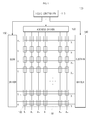
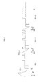
- FIG. 1 is a diagram illustrating an example of the arrangement of electrodes and connection among drivers in a plasma display device according to an embodiment of the invention
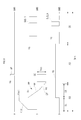
- FIG. 2 is a diagram illustrating an example of driving signals for driving the plasma display device according to the embodiment of the invention
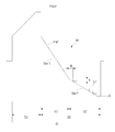
- FIG. 3 is a diagram illustrating a driving signal in a reset section shown in FIG. 2 ;
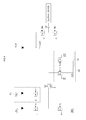
- FIG. 4 is a circuit diagram illustrating a driving circuit of a scan driver according to the embodiment of the invention.
- FIG. 5 is a diagram illustrating the waveform of a driving pulse including a sub-reset section having a step pulse therein.
- FIG. 1 is a diagram illustrating an example of the arrangement of electrodes and connection among drivers in a plasma display device according to an embodiment of the invention.
- FIG. 1 shows a single-scan-type display panel, and other types of display panels will be described later.
- the invention is not limited to the plasma display device shown in FIG. 1 .
- the plasma display device includes a logic controller 110, an address driver 120, a scan driver 130, a sustain driver 140, and a display panel 150.
- the logic controller 110 converts image signals transmitted from an image processor or the outside into data that can be processed by the drivers 120, 130, and 140. In addition, the logic controller 110 transmits data and control signals to the drivers 120, 130, and 140 to control the drivers 120, 130, and 140. In particular, the logic controller 110 controls the scanning driver 130 to apply a falling pulse comprising falling ramp pulse FRP and a step pulse SP connected the end of a falling ramp pulse FRP in a reset section RS, among driving signals supplied from the scan driver 130 to the display panel 150.
- the step pulse SP will be described below in more detail with reference to FIGS. 2 and 3 .
- the address driver 120 receives data and control signals from the logic controller 110 and supplies address pulses AP to address electrodes A (A1 to Am) of the display panel 150. Discharging cells 160 performing or not performing a display discharge are selected by the address pulses AP supplied from the address driver 120. In a selective write mode, the selected discharging cells perform the display discharge in an address section AS. Meanwhile, in a selective erase mode, the non-selected discharging cells perform the display discharge in the address section AP.
- the scan driver 130 receives data and control signals from the logic controller 110 and supplies reset pulses RP, scan pulses SC, and sustain pulses SUS to scan electrodes Y (Y1 to Yn) of the display panel 150.
- the scan driver 130 supplies a rising ramp pulse RRP that gradually rises and falling pulse comprising a falling ramp pulse that gradually falls and the step pulse SP at the end of the falling ramp pulse in the reset section RS.
- the scan driver 130 supplies the scan pulse SC in the address section AS in synchronization with the address pulse AP.
- the scan driver 130 supplies sustain pulses SUS_Y in a sustain section SS.
- the scan driver 130 supplies the falling pulse comprising the falling ramp pulse FRP and the step pulse SP to the display panel 150 under the control of the logic controller 110 to perform high-speed addressing while stably performing an address discharge. That is, the step pulse SP supplied from the scan driver 130 reduces the amount of visible light generated by discharge caused by the falling ramp pulse FRP. As a result, wall charges are efficiently erased, and thus an address voltage is lowered, making it possible to remarkably reduce the amount of heat generated from a connection member, which will be described in more detail with reference to FIGS. 2 and 3 .
- the sustain driver 140 supplies sustain pulses SUS_X in response to the data and control signals transmitted from the logic controller 110.
- the scan driver 130 and the sustain driver 140 supply the sustain pulses SUS_X, but the invention is not limited thereto.
- only the scan driver 130 may supply the sustain pulses.
- the sustain driver 140 may be integrated with the scan driver 130, which will be described later in more detail.
- the display panel 150 receives driving signals supplied from the address driver 120, the scan driver 130, and the sustain driver 140 to display images.
- the address electrodes A, the scan electrodes Y, and sustain electrodes X are formed on the display panel 150.
- the address driver 120 is arranged on one side of the display panel 150, and the address electrodes A and the address driver 120 are connected to each other by a connection member, particularly, a tape carrier package.
- the address electrodes A are formed in one direction, for example, in a vertical direction of the display panel 150.
- the scan electrodes Y and the sustain electrodes X are formed on the display panel 150 so as to intersect the address electrodes A.
- the scan electrodes Y and the sustain electrodes X are connected to the scan driver 130 and the sustain driver 140 by connection members, respectively.
- the discharging cells 160 are formed at intersections among the address electrodes A, the scan electrodes Y, and the sustain electrodes X.
- FIG. 2 is a diagram illustrating an example of a driving signal used to drive the plasma display device according to the embodiment of the invention.
- the driving signal supplied to the display panel 150 is divided into the reset section RS, the address section AS, and the sustain section SS.
- a rising ramp waveform RRP is applied to the scan electrode Y and a ground voltage GND is applied to the sustain electrode X and the address electrode A in a set-up section SU of the reset section RS where a sub-field SFn starts.
- a dark discharge is generated between the scan electrode Y and the other electrodes X and A in each discharging cell 160 by the rising ramp waveform RRP.
- the dark discharge causes positive wall charges to remain on the address electrode A and the sustain electrode X and negative wall charges to remain on the scan electrode Y.
- the falling ramp pulse FRP of the falling FP is applied to the scan electrode Y in a set-down section SD subsequent to the set-up section SU.
- a positive bias voltage Vb is applied to the sustain electrode X
- a ground voltage(GND) is applied to the address electrode A.
- the dark discharge is generated between the scan electrode Y and the address electrode X in each discharging cell 160 by the falling ramp pulse FRP, so that an excessively large amount of wall charges generated in the set-up section SU is adjusted to the amount of wall charges necessary for address discharge. Therefore, the distribution of wall charges in the discharging cell 160 is changed so as to be most suitable for the address discharge.
- the step pulse SP of the falling pulse FP is applied at the end of the set-down section SD.
- the step pulse SP starts from a voltage level lower than a ground voltage GND and is lowered to an erase voltage Ve.
- the erase voltage Ve may be equal to a scan voltage Vsc, which will be described later, and the erase voltage Ve may be variable.
- the step pulse SP makes it possible to supply the scan voltage Vsc at a low level, which makes it possible to lower the potential of the address pulse AP.
- a low scan voltage Vsc can be applied, which makes it possible to smoothly generate the address discharge without discharge delay and thus to drive the plasma display device at a high speed at a low address voltage Va.
- the supply of the step pulse SP makes it possible to increase the width of the reset pulse RP, prevent an erroneous discharge, and improve the stability of the address discharge, which will be described later in more detail with reference to FIG. 3 .
- a negative scan pulse SC is supplied to the scan electrode Y, and the address pulse AP is supplied in synchronization with the scan pulse SC.
- the discharging cell 160 is selected by the address pulse AP and the scan pulse SC.
- the voltage Va of the address pulse AP is lower than the address voltage Va according to the related art.
- the address driver 120 particularly, a driving chip of the tape carrier package can process the address pulse AP having a low address voltage. As a result, heat generated from the address driver is reduced, and the address driver can be stably driven. Meanwhile, a bias voltage Vb can be continuously supplied to the sustain electrode X in the address section AS as well as in the set-down section SD.
- the sustain pulses SUS_Y and X having a positive sustain voltage Vs are alternately applied to the scan electrode Y and the sustain electrode X in the sustain section SS. Therefore, the selected discharging cell 160 performs a display discharge in the address section AS.
- FIG. 3 is a diagram illustrating a driving pulse in the reset section shown in FIG. 2 .
- the address voltage Va and the scan voltage Vsc are lower than those in the related art. Therefore, the plasma display device and a method of driving the same according to the embodiments of the invention can perform high-speed addressing at a low address voltage Va.
- discharge is generated when the difference between a wall charge voltage formed by wall charges and a voltage formed by the falling ramp pulse FRP is higher than a discharge voltage in a portion of the set-down section SD in which the voltage applied to the scan electrode is reduced at a constant gradient in the reset section of the falling ramp pulse FRP, as shown in FIG. 3 .
- the reduction rate of the wall charge voltage is approximately equal to that of the falling ramp pulse FRP.
- the difference between the wall charge voltage and the voltage formed by the falling ramp pulse FRP is maintained at a sufficient level to generate discharge, and thus discharge is continuously generated. Therefore, most of the wall charges except the wall charges necessary for the address discharge are erased, and the environment of the discharging cell is initialized.
- the internal environment of the discharging cells that has performed the display discharge in the previous sub-field is different from that of the discharging cells that have not performed the display discharge in the previous sub-field.
- the difference in internal environment affects the address discharge, which causes a problem in that no discharging cell is selected or unnecessary discharging cells are selected.
- the distribution of wall charges in the discharging cells becomes non-uniform, which makes it necessary to increase the address voltage or the scan voltage of the scan pulse SC.
- the address pulse AP is supplied together with the scan pulse SC in order to minimize the discharge delay.
- the difference between the voltage of the address pulse AP and the voltage of the scan pulse SC is higher than a firing voltage Vf, the address discharge is generated.
- the falling ramp pulse FRP and the step pulse SP of the falling pulse FP have different gradients in two sections.
- the set-down section SD is divided into a first section R1 in which the falling ramp pulse FRP has a first gradient Ver1 and a second section R2 in which the falling ramp pulse FRP has a second gradient Ver2.
- the first gradient Ver1 of the first section R1 may be equal to or different from the second gradient Ver2 of the second section R2 according to operational conditions.
- the second gradient Ver2 may be larger than the first gradient Ver1 in order to increase the amount of wall charges to be erased.
- the second gradient Ver2 may be smaller than the first gradient Ver1 in order to decrease the amount of wall charges to be erased. That is, the first and second gradients Ver1 and Ver2 depend on unique characteristics of a plasma display device, and the invention is not limited to the above-mentioned relationship between the first and second gradients Ver1 and Ver2.
- the wall charges excessively generated in the set-up section SU are erased in the set-down section SD.
- the voltage formed by the wall charges is lower than the voltage formed by the falling ramp pulse FRP in a predetermined portion of the first section R1.
- the wall charges are recombined and energy is released.
- the discharge causes the reduction rate of the voltage formed by the wall charges to be substantially equal to that of the voltage formed by the falling ramp pulse FRP. That is, the discharge causes the gradient of the voltage formed by the wall charges to be equal to the first gradient Ver1.
- the gradient of the second section R2 is adjusted to be smaller than that of the first section R1 in order to leave some of the wall charges without erasing all of the wall charges.
- the time when the second section R2 is applied may be adjusted arbitrarily.
- the second section R2 may be applied at a point of time when the supply of power from a power supply for supplying a falling ramp pulse having the first section R1 stops.
- the falling ramp pulse FRP having the second gradient Ver2 in the second section R2 is supplied, an erase discharge stops or is reduced by the falling ramp pulse FRP having a gradient lower than a reduction gradient of the wall charge voltage. Then, all of the wall charges are not completely erased, but some of the wall charges remain. The remaining wall charges assist the address discharge in the subsequent address section AS.
- the erase rate of the wall charges should be increased in order to prevent an erroneous discharge.
- the second gradient Ver2 is adjusted to be larger than the first gradient Ver1 in order to increase the erase rate of the wall charges.
- the width W is a power-off section
- the height H is a power-on section.
- FIG. 4 is a circuit diagram illustrating the structure of a driving circuit of the scan driver according to the embodiment of the invention.
- the structure of the driving circuit shown in FIG. 4 is just illustrative, but is not limitative.
- the structure of the driving circuit will be described with reference to FIGS. 2 and 3 as well as FIG. 4 .
- a sustain switch Ys, a node switch Ypn, and a low switch SW L are turned on, and a sustain voltage(or called a first voltage) Vs is applied to a panel Cp.
- a rising ramp switch Yrr is turned on under the control of a rising ramp pulse supply unit RR, and a reset high voltage Vset is applied to the panel Cp. Then, the rising ramp pulse RRP that rises gradually is supplied to the panel Cp.
- the rising ramp switch Yrr is turned off to cut the supply of the reset high voltage Vset, and the sustain switch Ys is turned off to cut the supply of the sustain voltage Vs.
- a first supply unit FR turns on a falling ramp switch(or called a first switch) Yfr to supply the scan voltage(or called a second voltage) Vsc, which is a reset low voltage, to the panel Cp, and the falling ramp pulse FRP that falls gradually is supplied to the panel Cp.
- the first supply unit FR includes a falling ramp controller CF controlling the falling ramp switch Yfr.
- a scan switch(or called a second switch) Ysc is switched by a second supply unit ST such that a step pulse having the second gradient Ver2 is supplied to the panel Cp.
- the second supply unit ST includes a step pulse controller CS controlling the scan switch Ysc.
- a separate power supply is not used to supply power to the panel Cp through the scan switch Ysc, but the scan voltage Vsc is supplied to the panel Cp through the scan switch Ysc.
- the scan voltage Vsc is generated from the first power supply.
- FIG. 5 is a waveform diagram illustrating a driving waveform including sub-reset sections each having the step pulse. A continuous series of three sub-fields is shown in FIG. 5 , and a main reset section and sub-reset sections are mixed in the three sub-fields.
- the step pulse SP can be applied to a sub-reset section SR1 as well as a falling ramp pulse in a main reset section MR.
- a voltage having the same waveform as the falling ramp pulse FRP of the main reset section MR is applied immediately after the last sustain pulse SUS_L to initialize the discharging cell. Therefore, the falling ramp pulse FRP can be applied to the sub-reset section SR1 as well as the main reset section MR.
- the sub-reset section SR1 including the step pulse SP be selectively applied to a sub-field SFn+1 having a large grey weight value.
- the sub-reset section SR1 including the step pulse SP serves as the set-up section SU of the main reset section MR in the sub-field SFn+1 having a large grey weight value, which makes it unnecessary to additionally provide the set-up section SU in the sub-field SFn+1 having a large grey weight value. Therefore, the sub-reset section SR1, not the main reset section MR, is provided after the display discharge in the sub-field SFn+1 having a large grey weight value to initialize the internal environment of the discharging cell as in the main reset section MR.
- the grey weight value becomes larger, a larger amount of wall charge can be generated in the sub-reset section SR1 than in the set-up section of the main reset section. Therefore, an erase pulse plays an important role in the generation of wall charges, and thus it is preferable to apply the falling ramp pulse FRP including the step pulse SP in the sub-field SFn+1 having a large grey weight value.
- the falling pulse FP having the step pulse SP may be applied to all of the sub-reset sections SR. However, it is preferable to apply the falling pulse FP comprising the step pulse SP to only some sub-fields SFn and SFn+1, if necessary, as shown in FIG. 5 , but the invention is not limited thereto.
- a reset waveform including a step pulse is used, which makes it possible to stably perform high-speed addressing at a low voltage without deteriorating a display quality.
Landscapes
- Engineering & Computer Science (AREA)
- Physics & Mathematics (AREA)
- Computer Hardware Design (AREA)
- General Physics & Mathematics (AREA)
- Theoretical Computer Science (AREA)
- Power Engineering (AREA)
- Plasma & Fusion (AREA)
- Control Of Indicators Other Than Cathode Ray Tubes (AREA)
- Control Of Gas Discharge Display Tubes (AREA)
Applications Claiming Priority (1)
| Application Number | Priority Date | Filing Date | Title |
|---|---|---|---|
| KR1020070131357A KR20090063847A (ko) | 2007-12-14 | 2007-12-14 | 플라즈마 디스플레이 장치 및 이의 구동 방법 |
Publications (1)
| Publication Number | Publication Date |
|---|---|
| EP2073189A1 true EP2073189A1 (fr) | 2009-06-24 |
Family
ID=40269645
Family Applications (1)
| Application Number | Title | Priority Date | Filing Date |
|---|---|---|---|
| EP08171490A Withdrawn EP2073189A1 (fr) | 2007-12-14 | 2008-12-12 | Dispositif à plasma et son procédé de commande |
Country Status (5)
| Country | Link |
|---|---|
| US (1) | US20090153443A1 (fr) |
| EP (1) | EP2073189A1 (fr) |
| JP (1) | JP2009145886A (fr) |
| KR (1) | KR20090063847A (fr) |
| CN (1) | CN101458894A (fr) |
Families Citing this family (1)
| Publication number | Priority date | Publication date | Assignee | Title |
|---|---|---|---|---|
| US20250159879A1 (en) * | 2023-11-14 | 2025-05-15 | Ememory Technology Inc. | Non-volatile memory device for low operation voltage |
Citations (4)
| Publication number | Priority date | Publication date | Assignee | Title |
|---|---|---|---|---|
| EP1533781A2 (fr) * | 2003-11-21 | 2005-05-25 | Lg Electronics Inc. | Méthode et dispositif de commande d'un panneau d'affichage à plasma |
| EP1580713A2 (fr) * | 2004-03-15 | 2005-09-28 | Samsung SDI Co., Ltd. | Dispositif et procédé de pilotage d'un panneau d'affichage à plasma et dispositif d'affichage à plasma |
| US20050280024A1 (en) * | 2004-05-20 | 2005-12-22 | Jin-Sung Kim | Plasma display panel and driving method thereof |
| US20060164340A1 (en) * | 2003-05-14 | 2006-07-27 | Samsung Sdi Co., Ltd. | Plasma display panel and method for driving the same |
-
2007
- 2007-12-14 KR KR1020070131357A patent/KR20090063847A/ko not_active Ceased
-
2008
- 2008-12-01 JP JP2008306606A patent/JP2009145886A/ja not_active Withdrawn
- 2008-12-12 EP EP08171490A patent/EP2073189A1/fr not_active Withdrawn
- 2008-12-12 CN CNA2008101840326A patent/CN101458894A/zh active Pending
- 2008-12-12 US US12/333,671 patent/US20090153443A1/en not_active Abandoned
Patent Citations (4)
| Publication number | Priority date | Publication date | Assignee | Title |
|---|---|---|---|---|
| US20060164340A1 (en) * | 2003-05-14 | 2006-07-27 | Samsung Sdi Co., Ltd. | Plasma display panel and method for driving the same |
| EP1533781A2 (fr) * | 2003-11-21 | 2005-05-25 | Lg Electronics Inc. | Méthode et dispositif de commande d'un panneau d'affichage à plasma |
| EP1580713A2 (fr) * | 2004-03-15 | 2005-09-28 | Samsung SDI Co., Ltd. | Dispositif et procédé de pilotage d'un panneau d'affichage à plasma et dispositif d'affichage à plasma |
| US20050280024A1 (en) * | 2004-05-20 | 2005-12-22 | Jin-Sung Kim | Plasma display panel and driving method thereof |
Also Published As
| Publication number | Publication date |
|---|---|
| JP2009145886A (ja) | 2009-07-02 |
| CN101458894A (zh) | 2009-06-17 |
| KR20090063847A (ko) | 2009-06-18 |
| US20090153443A1 (en) | 2009-06-18 |
Similar Documents
| Publication | Publication Date | Title |
|---|---|---|
| JP4100338B2 (ja) | プラズマディスプレイパネルの駆動方法 | |
| JP2006195488A (ja) | 高コントラストプラズマディスプレイ | |
| JP2003330411A (ja) | プラズマディスプレイパネルの駆動方法及び装置 | |
| JP4100337B2 (ja) | プラズマディスプレイパネルの駆動方法 | |
| JP4050286B2 (ja) | プラズマディスプレイ装置及びその駆動方法 | |
| US20040164931A1 (en) | Plasma display and method of driving the same | |
| EP2073189A1 (fr) | Dispositif à plasma et son procédé de commande | |
| KR100884535B1 (ko) | 플라즈마 표시 장치 및 그 구동 방법 | |
| KR100627412B1 (ko) | 플라즈마 표시 장치 및 그 구동 방법 | |
| EP1777683A2 (fr) | Procédé de commande de panneau d'affichage à plasma | |
| JP2007072464A (ja) | プラズマディスプレイ装置及びプラズマディスプレイ装置の駆動方法 | |
| KR100739079B1 (ko) | 플라즈마 표시 장치 및 그 구동 방법 | |
| KR100570690B1 (ko) | 플라즈마 표시장치의 구동방법. | |
| KR100551040B1 (ko) | 플라즈마 표시 패널의 구동 방법 및 플라즈마 표시 장치 | |
| KR20070091426A (ko) | 플라즈마 표시 장치 및 그 구동방법 | |
| KR100542517B1 (ko) | 플라즈마 표시 패널 및 그의 구동방법 | |
| KR100740095B1 (ko) | 플라즈마 표시 장치 및 그 구동 방법 | |
| KR100649258B1 (ko) | 플라즈마 표시 장치 및 그 구동 방법 | |
| JP2006133738A (ja) | プラズマディスプレイ装置およびその駆動方法 | |
| KR100726662B1 (ko) | 플라즈마 디스플레이 패널의 구동 장치 | |
| KR100786863B1 (ko) | 플라즈마 표시 장치 및 그 구동 방법 | |
| KR100778448B1 (ko) | 플라즈마 표시 장치 및 그 구동 방법 | |
| KR20050077823A (ko) | 휘도를 보상할 수 있는 플라즈마 표시 패널의 구동 방법 | |
| KR20060034808A (ko) | 플라즈마 표시 장치 및 그 구동 방법 | |
| US20070273616A1 (en) | Driving method for plasma display apparatus |
Legal Events
| Date | Code | Title | Description |
|---|---|---|---|
| PUAI | Public reference made under article 153(3) epc to a published international application that has entered the european phase |
Free format text: ORIGINAL CODE: 0009012 |
|
| 17P | Request for examination filed |
Effective date: 20081213 |
|
| AK | Designated contracting states |
Kind code of ref document: A1 Designated state(s): AT BE BG CH CY CZ DE DK EE ES FI FR GB GR HR HU IE IS IT LI LT LU LV MC MT NL NO PL PT RO SE SI SK TR |
|
| AX | Request for extension of the european patent |
Extension state: AL BA MK RS |
|
| 17Q | First examination report despatched |
Effective date: 20090721 |
|
| AKX | Designation fees paid |
Designated state(s): DE FR GB HU |
|
| STAA | Information on the status of an ep patent application or granted ep patent |
Free format text: STATUS: THE APPLICATION IS DEEMED TO BE WITHDRAWN |
|
| 18D | Application deemed to be withdrawn |
Effective date: 20091201 |