EP2073310B1 - Système d'antenne réseau et son module d'émission-réception - Google Patents
Système d'antenne réseau et son module d'émission-réception Download PDFInfo
- Publication number
- EP2073310B1 EP2073310B1 EP08253794.5A EP08253794A EP2073310B1 EP 2073310 B1 EP2073310 B1 EP 2073310B1 EP 08253794 A EP08253794 A EP 08253794A EP 2073310 B1 EP2073310 B1 EP 2073310B1
- Authority
- EP
- European Patent Office
- Prior art keywords
- transmitting
- transmit
- terminal
- element antennas
- receiving
- Prior art date
- Legal status (The legal status is an assumption and is not a legal conclusion. Google has not performed a legal analysis and makes no representation as to the accuracy of the status listed.)
- Not-in-force
Links
- 230000010363 phase shift Effects 0.000 claims description 15
- 230000002194 synthesizing effect Effects 0.000 description 9
- 230000005540 biological transmission Effects 0.000 description 5
- 238000010586 diagram Methods 0.000 description 3
- 238000010276 construction Methods 0.000 description 1
- 230000007423 decrease Effects 0.000 description 1
- 230000000593 degrading effect Effects 0.000 description 1
- 238000002955 isolation Methods 0.000 description 1
- 238000012986 modification Methods 0.000 description 1
- 230000004048 modification Effects 0.000 description 1
- 231100000989 no adverse effect Toxicity 0.000 description 1
Images

Classifications
-
- H—ELECTRICITY
- H01—ELECTRIC ELEMENTS
- H01Q—ANTENNAS, i.e. RADIO AERIALS
- H01Q3/00—Arrangements for changing or varying the orientation or the shape of the directional pattern of the waves radiated from an antenna or antenna system
- H01Q3/26—Arrangements for changing or varying the orientation or the shape of the directional pattern of the waves radiated from an antenna or antenna system varying the relative phase or relative amplitude of energisation between two or more active radiating elements; varying the distribution of energy across a radiating aperture
- H01Q3/30—Arrangements for changing or varying the orientation or the shape of the directional pattern of the waves radiated from an antenna or antenna system varying the relative phase or relative amplitude of energisation between two or more active radiating elements; varying the distribution of energy across a radiating aperture varying the relative phase between the radiating elements of an array
- H01Q3/34—Arrangements for changing or varying the orientation or the shape of the directional pattern of the waves radiated from an antenna or antenna system varying the relative phase or relative amplitude of energisation between two or more active radiating elements; varying the distribution of energy across a radiating aperture varying the relative phase between the radiating elements of an array by electrical means
- H01Q3/36—Arrangements for changing or varying the orientation or the shape of the directional pattern of the waves radiated from an antenna or antenna system varying the relative phase or relative amplitude of energisation between two or more active radiating elements; varying the distribution of energy across a radiating aperture varying the relative phase between the radiating elements of an array by electrical means with variable phase-shifters
-
- H—ELECTRICITY
- H01—ELECTRIC ELEMENTS
- H01Q—ANTENNAS, i.e. RADIO AERIALS
- H01Q21/00—Antenna arrays or systems
- H01Q21/0006—Particular feeding systems
Definitions
- the present invention relates to an array antenna system and a transmit/receive module thereof for use as a radar apparatus and the like.
- An electronic scan-type array antenna system that has a plurality of two-dimensionally arrayed element antennas and that scans by changing a transmitting directivity of pulse signals transmitted from those element antennas and a receiving directivity of their reflected waves by way of phase control has been used as a radar apparatus and the like.
- a unitary unit is formed by units having transmitting and receiving paths connected to one element antenna through a circulator.
- FIG. 1 shows a prior art exemplary structure in which a transmitting/receiving unit is formed by combining two unitary units for example.
- Each of a plurality of, e.g., five, transmit/receive modules 31 is connected with element antennas 32a and 32b in the array antenna system 30.
- the transmit/receive module 31 is composed of two unitary units 31a and 31b having the same structure from each other.
- the unitary unit 31a has a three-terminal circulator 41a having terminals A, B and C, a receiving amplifier 42a, a receiving phase shifter 43a, a transmitting phase shifter 44a and a transmitting amplifier 45a.
- a transmitting signal sent from a transmitting signal generating section 34 is distributed by a transmitting signal distributing section 33.
- the transmitting phase shifter 44a applies a phase shift amount controlled by a transmitting/receiving phase control section 38 to the transmitting signal and the transmitting amplifier 45a amplifies it.
- the signal is then input to the three-terminal circulator 41a and is transmitted from the element antenna 32a.
- a received signal processing section 36 electrically conducts image processing on the synthesized signal and an image displaying section 37 displays a radar image. The same applies also to the unitary unit 31b.
- This prior art array antenna system 30 has had a problem that it requires the transmission phase shifters 44a and 44b and the transmission amplifiers 45a and 45b because it has the receiving and transmitting paths per each of the unitary units 31a and 31b.
- the unitary unit 31b it is conceivable to form one of the unitary units, e.g., the unitary unit 31b, close to the both ends of the apparatus to have only the receiving path in order to reduce the transmission phase shifters 44a and 44b and the transmitting amplifiers45a and 45b.
- the antenna system is constructed as such, there have been problems that an apparent size as an antenna becomes small and an antenna gain drops, degrading in performance as an antenna system.
- the present invention is a transmit/receive module as defined in claim 1, and an array antenna system including such modules.
- the present invention can provide an array antenna system and its transmit/receive module whose cost may be reduced as a whole by reducing circuits of a transmitting path without dropping a transmitting antenna gain.
- an array antenna system has a plurality of arrayed element antennas and transmit/receive modules that are respectively connected with those element antennas and that respectively apply a predetermined phase shift amount to transmitting signals to be supplied to the element antennas and to received signals received by the element antennas, wherein the transmit/receive module has one transmitting path that is connected to the first and second element antennas and that amplifies and distributes the transmitting signal to the first and second element antennas after applying a predetermined transmitting phase shift amount and two receiving paths that respectively amplify and apply a receiving phase shift amount to the received signals received from the first and second element antennas.
- the circuits of the transmitting path may be cut and the cost may be lowered as a whole without lowering the transmitting antenna gain.
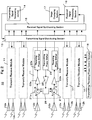
- FIG. 2 is a diagram showing an overall structure of an array antenna system according to one embodiment of the invention when it is applied as a radar apparatus.
- This array antenna system 10 has a plurality of transmit/receive modules 11, two element antennas 12a and 12b connected respectively to each transmit/receive module 11, a transmitting signal distributing section 13 connected to a transmitting path of the transmit/receive module 11, a transmitting signal generating section 14 that supplies transmitting signals to the transmitting signal distributing section 13, a received signal synthesizing section 15 for synthesizing received signals obtained through a receiving path of the transmit/receive module 11, a received signal processing section 16 for performing image processing and others on the received signal synthesized in the received signal synthesizing section 15, an image displaying section 17 for displaying the signal processed in the received signal processing section 16 and a transmitting/receiving phase control section 18 for controlling phase shift amounts of a transmitting phase shifter and a receiving phase shifter described later within each transmit/receive module 11.
- the transmit/receive module 11 has one transmitting path and two receiving paths. Specifically, the transmit/receive module 11 has a three-terminal circulator 21a whose terminal A is connected to the element antenna 12a, a receiving amplifier 22a whose input terminal is connected to a terminal B of the three-terminal circulator 21a, a receiving phase shifter 23a whose input terminal is connected with an output terminal of the receiving amplifier 22a and whose output terminal is connected with the received signal synthesizing section 15 described above, a three-terminal circulator 21b whose terminal A is connected to the element antenna 12b, a receiving amplifier 22b whose input terminal is connected to a terminal C of the three-terminal circulator 21b, a receiving phase shifter 23b whose input terminal is connected with an output terminal of the receiving amplifier 22b and whose output terminal is connected with the received signal synthesizing section 15 described above, a transmitting phase shifter 24 that is connected with an output terminal of the transmitting signal distributing section 13, a transmitting amplifier 25 whose input terminal
- the receiving amplifiers 22a and 22b and the transmitting amplifier 25 are composed of Monolithic Microwave Integrated Circuits (MMIC) for example.
- MMIC Monolithic Microwave Integrated Circuits
- a Y-shaped distributor composed of a planar microwave IC proposed by Wilkinson (here, this distributor will be also referred to as the Wilkinson-type distributor) may be used for example as the bi-distributor 26.
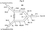
- FIG. 3 shows a shape of a micro-strip line of one exemplary Y-shaped distributor used in the transmit/receive module 11 of the embodiment described above.
- a micro-strip line ML1 whose one end is a terminal PT1 is divided at point P1 into micro-strip lines ML12 and ML13.
- the micro-strip lines are then bent at points P12 and P13 as micro-strip lines ML22 and ML33 that are parallel to each other and are bent outwardly at next points P22 and P33 to be formed as micro-strip lines ML2 and ML3.
- Other ends of the micro-strip lines ML2 and ML3 are formed as terminals PT2 and PT3, respectively.
- a resistance R is then connected between the points P22 and P33.
- a signal input from the terminal PT1 is output to the terminals PT2 and PT3 by being divided with a predetermined ratio, e.g., equally. That is, an output from the terminal PT2 is input to the terminal C of the three-terminal circulator 21a and is output from the terminal A of this circulator 21a. Meanwhile, an output from the terminal PT3 is input to the terminal B of the three-terminal circulator 21b and is output from the terminal A of this circulator 21b.
- terminals PT2 and PT3 are connected respectively to the three-terminal circulators 21a and 21b in the present embodiment, substantially there is no input from the three-terminal circulators 21a and 21b to the terminals PT2 and PT3.
- the three-terminal circulator 21a has an electrical characteristic of sending a signal input from the terminal A to the terminal B, of sending a signal input from the terminal B to the terminal C and of sending a signal input from the terminal C to the terminal A.
- the three-terminal circulator 21b also has an electrical characteristic of sending a signal input from the terminal A to the terminal C, of sending a signal input from the terminal C to the terminal B and of sending a signal input from the terminal B to the terminal A. Accordingly, the transmitting signal distributed in the bi-distributor 26 and input to the terminal C of the three-terminal circulator 21a is supplied to the element antenna 12a connected to the terminal A of the three-terminal circulator 21a and is transmitted. Meanwhile, the transmitting signal supplied from the bi-distributor 26 to the terminal B of the three-terminal circulator 21b is supplied to the element antenna 12b connected to the terminal A and is transmitted.
- a signal received by the element antenna 12a is supplied to the terminal A of the three-terminal circulator 21a and is output from the terminal B to be supplied to the receiving amplifier 22a.
- a signal received by the element antenna 12b is supplied to the terminal A of the three-terminal circulator 21b and is output from the terminal C to be supplied to the receiving amplifier 22b.
- the three-terminal circulators 21a and 21b having such characteristics that rotation directions of input signals are reversed from each other may be obtained just by changing polarities of magnets provided upper and lower parts of the circulators while keeping components other than the magnets the same.
- FIG. 2 shows the system having only the five transmit/receive modules 11 in a row in order to facilitate understanding thereof, an actual system is normally provided with many more transmit/receive modules arrayed even two-dimensionally.
- a transmitting signal e.g., a pulse signal, generated by the transmitting signal generating section 14 is supplied to the transmitting signal distributing section 13 and is sent from the transmitting signal distributing section 13 to the transmitting phase shifter 24 of each transmit/receive module 11.
- the transmitting phase shifter 24 applies a predetermined phase shift amount (delay amount) to the transmitting signal based on a phase control signal sent from the transmitting/receiving phase control section 18 and sends the signal to the transmitting amplifier 25 to amplify the same.
- the transmitting signal provided with the predetermined phase shift amount and amplified is supplied to the bi-distributor 26 to be distributed substantially equally to the terminals C and B of the three-terminal circulators 21a and 21b.
- the transmitting signal supplied from the bi-distributor 26 to the terminal C of the three-terminal circulator 21a is output out of the terminal A to be transmitted from the element antenna 12a. Meanwhile, the transmitting signal supplied from the bi-distributor 26 to the terminal B of the three-terminal circulator 21b is output out of the terminal A and is transmitted from the element antenna 12b.
- the transmitting signal transmitted from the element antenna 12a has the same phase with the transmitting signal transmitted from the element antenna 12b. While different phases are applied to the transmitting signals between neighboring transmit/receive modules in electronically scanning the transmitting signals in general, the transmitting signals having the same phase are transmitted from the antennas 12a and 12b connected to one transmit/receive module. That is, the received signals having the equal phase are transmitted from the antennas 12a and 12b in a direction perpendicular to the array of those antennas.
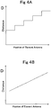
- the transmitting signal has a step-like phase plane as shown in FIG. 4A as a whole.
- FIG. 4A shows a distance D by an axis of ordinate and each position of the element antenna by an axis of abscissas. Accordingly, it signifies the same phase plane of the transmitting signals transmitted from the respective element antennas.
- the phase plane of the radio transmitted from the element antenna is shown extremely clearly in FIG. 4A . Accordingly, the step-like portion of the boundary between the phase plane of the radio waves transmitted with equal phase from the pair of antennas and that of the radio waves transmitted with equal phase from a neighboring pair of element antennas is conspicuous. However, because a number of the transmit/receive modules is actually so large as several tens or more, the stepped-like portions give substantially no adverse effect to the transmitting characteristics.
- the respective antennas 12a and 12b receive reflected waves of the radar transmitting signals transmitted as described above and returned from each object.
- the radar-receiving signal received by each element antenna 12a is input to the terminal A of the three-terminal circulator 21a. Then, the radar-receiving signal is output out of the terminal B of the three-terminal circulator 21a and is input to an input terminal of the receiving amplifier 22a to be amplified.
- the receiving phase shifter 23a applies a phase shift amount controlled by the transmitting/receiving phase control section 18 to the received signal amplified by the receiving amplifier 22a and supplies the signal to the received signal synthesizing section 15.
- the radar-receiving signal received by each element antenna 12b is input to the terminal A of the three-terminal circulator 21b. Then, the radar-receiving signal is output out of the terminal C of the three-terminal circulator 21b and is input to an input terminal of the receiving amplifier 22b to be amplified.
- the receiving phase shifter 23b applies a phase shift amount controlled by the transmitting/receiving phase control section 18 to the received signal amplified by the receiving amplifier 22b and supplies the signal to the received signal synthesizing section 15.
- the receiving phase shifter 23a corresponding to the element antenna 12a is different from the receiving phase shifter 23b corresponding to the element antenna 12b in the case of the receiving. Accordingly, the transmitting/receiving phase control section 18 can apply different phase shift amounts to the both receiving phase shifters 23a and 23b within the same transmit/receive module 11, so that the same phase plane in receiving has substantially a linear characteristic as shown in FIG. 4B.
- FIG. 4B shows a distance D by an axis of ordinate and each position of the element antenna by an axis of abscissas.
- the received signal processing section 16 performs the image processing on the received signal synthesized by the received signal synthesizing section 15 to display on a radar display screen of the image display section 17.
- the present invention is applicable also to an array antenna system in which the element antennas are two-dimensionally disposed and having much more element antennas and transmit/receive modules.
- each transmit/receive module of the array antenna system of the invention requires the distributor and one high-output transmitting amplifier as compared to that of the prior art antenna system, each transmit/receive module requires only one transmitting path. That is, it becomes possible to eliminate one each of the transmitting amplifiers and the transmitting phase shifters.
- transmit/receive modules e.g., about ten modules
- transmit/receive modules composed of the same unitary units are disposed at a center part of the antenna system
- transmit/receive modules whose one unitary unit is composed of only a receiving path are disposed at both ends (e.g., about 15 modules each) of the apparatus.
- the prior art antenna system described above is composed of the 20 transmit/receive two-channel modules at the center part and of the array antenna system 30 transmit/receive one-channel modules at the both ends.
- a transmitting antenna gain improves by about 3 dB. Because the number of the transmitting element antennas decreases from 50 to 40, transmitting electric power drops by about 1 dB. As a result, the transmitting antenna gain improves by about 2 dB. Still more, an interval (interval where phase control can be made) in a transmitting elevation (EL) direction is doubled as compared to the case of the prior art apparatus described above and a transmitting EL scan range may be run over by ⁇ 4°.
- EL transmitting elevation
- the invention has an advantage of keeping the characteristics of the apparatus without dropping the transmitting antenna gain. Still more, because the invention allows the transmitting amplifier and the transmitting phase shifter of the transmitting path to be cut, it allows the transmit/receive module to be downsized and the cost of the transmit/receive module to be lowered. Consequently, the invention has such merits that it allows the array antenna system to be downsized and the cost of the apparatus to be lowered.
- distributors other than the Y-shaped distributor may be used.
- the distributor is not also limited to the bi-distributor.
- the distributor is not limited to the Wilkinson-type and a distributor through which signals pass with substantially equal phase may be used as the bi-distributor of the invention.
- the invention is not limited to that having the three terminals.
- the invention is not also limited to the circulator and may use a signal switch that automatically switches transmitting and receiving paths.
- the path of the transmitting phase shifter 24, the transmitting amplifier 25 and the be-distributor 26, i.e., the part of the transmitting path and the path of the receiving amplifier 22a, the receiving phase shifter 23a or of the receiving amplifier 22b and the receiving phase shifter 23b, i.e., the part of the receiving path, have formed the separate paths in the embodiment described above as shown in FIG. 2 .
- the invention may be arranged so as to overlap the part of the transmitting path with the part of the receiving path and to switch the paths temporally. That is, the transmitting phase shifter 24 may be used also as the receiving phase shifter 23a or the receiving phase shifter 23b so as to switch during transmission and receiving by means of a switch. Although such arrangement requires the switch, the number of the phase shifters, e.g., three in the case of the transmit/receive module of the embodiment shown in FIG. 2 , may be reduced further to two.
Landscapes
- Variable-Direction Aerials And Aerial Arrays (AREA)
- Radar Systems Or Details Thereof (AREA)
Claims (5)
- Module de transmission/réception pour un ensemble d'antennes comprenant une pluralité desdits modules en parallèle et qui, lors de l'utilisation, est connecté avec des premier et deuxième éléments d'antennes et qui applique une valeur de décalage de phase prédéterminée aux signaux de transmission à fournir aux éléments d'antennes et aux signaux de réception reçus par les éléments d'antennes, le module de transmission/réception comprenant :un premier et un deuxième commutateur de signaux (21a, 21b) pour une connexion respectivement avec les premier et deuxième éléments d'antennes (12a, 12b) ;un dispositif de décalage de phase de transmission (24) permettant d'appliquer une valeur de décalage de phase prédéterminée au signal de transmission et pour transmettre avec la même phase appliquée au premier et au deuxième éléments d'antennes ;un amplificateur de transmission (25) permettant d'amplifier le signal de transmission auquel la valeur de décalage de phase prédéterminée a été appliquée par le dispositif de décalage de phase de transmission ;un distributeur (26) permettant de distribuer le signal de transmission amplifié par l'amplificateur de transmission au premier et au deuxième commutateur de signaux (21a, 21b) ;des premier et deuxième amplificateurs de réception (22a, 22b) qui sont connectés au premier et au deuxième commutateur de signaux pour amplifier respectivement les signaux reçus par le premier et le deuxième élément d'antennes ; etdes premier et deuxième dispositifs de décalage de phase de réception (23a, 23b) permettant d'appliquer une valeur de décalage de phase prédéterminée respectivement aux signaux reçus amplifiés par les premier et deuxième amplificateurs de réception avec différentes phases de réception appliquées aux premier et deuxième éléments d'antennes.
- Module de transmission/réception selon la revendication 1, dans lequel les premier et deuxième commutateurs de signaux (21a, 21b) sont des circulateurs dont les directions de rotation des signaux sont opposées entre elles.
- Module de transmission/réception selon la revendication 1 ou 2, dans lequel le distributeur (26) est un distributeur à deux sorties dont les phases provisoires sont essentiellement égales.
- Module de transmission/réception selon la revendication 3, dans lequel le distributeur (26) est un distributeur de type Wilkinson.
- Système d'ensemble d'antennes (10) comprenant une pluralité d'éléments d'antennes en réseau et de modules de transmission/réception qui sont connectés avec les éléments d'antennes et qui sont conçus pour appliquer une valeur de décalage de phase prédéterminée aux signaux de transmission à fournir aux éléments d'antennes et aux signaux reçus par les éléments d'antennes,
chaque module de transmission/réception étant conforme aux revendications précédentes.
Applications Claiming Priority (1)
| Application Number | Priority Date | Filing Date | Title |
|---|---|---|---|
| JP2007326183A JP4521440B2 (ja) | 2007-12-18 | 2007-12-18 | アレイアンテナ装置及びその送受信モジュール |
Publications (2)
| Publication Number | Publication Date |
|---|---|
| EP2073310A1 EP2073310A1 (fr) | 2009-06-24 |
| EP2073310B1 true EP2073310B1 (fr) | 2017-01-04 |
Family
ID=40521764
Family Applications (1)
| Application Number | Title | Priority Date | Filing Date |
|---|---|---|---|
| EP08253794.5A Not-in-force EP2073310B1 (fr) | 2007-12-18 | 2008-11-24 | Système d'antenne réseau et son module d'émission-réception |
Country Status (3)
| Country | Link |
|---|---|
| US (1) | US8259686B2 (fr) |
| EP (1) | EP2073310B1 (fr) |
| JP (1) | JP4521440B2 (fr) |
Families Citing this family (3)
| Publication number | Priority date | Publication date | Assignee | Title |
|---|---|---|---|---|
| DE102010001761A1 (de) * | 2010-02-10 | 2011-08-11 | Robert Bosch GmbH, 70469 | Radarsensor |
| JP2012222725A (ja) | 2011-04-13 | 2012-11-12 | Toshiba Corp | アクティブアレイアンテナ装置 |
| US9742075B2 (en) * | 2015-08-09 | 2017-08-22 | The United States Of America As Represented By The Secretary Of The Navy | System including a hybrid active array |
Citations (1)
| Publication number | Priority date | Publication date | Assignee | Title |
|---|---|---|---|---|
| EP0132378A2 (fr) * | 1983-07-21 | 1985-01-30 | Nec Corporation | Dispositif radar à balayage avec faisceaux multiples |
Family Cites Families (24)
| Publication number | Priority date | Publication date | Assignee | Title |
|---|---|---|---|---|
| US3978482A (en) * | 1975-03-24 | 1976-08-31 | Hughes Aircraft Company | Dynamically focused thinned array |
| JPS6170802A (ja) * | 1984-09-13 | 1986-04-11 | Mitsubishi Electric Corp | アンテナ装置 |
| JPH01129509A (ja) * | 1987-11-16 | 1989-05-22 | Toshiba Corp | アレーアンテナ装置 |
| JP2795866B2 (ja) * | 1989-01-20 | 1998-09-10 | 株式会社東芝 | アレイアンテナ装置 |
| JP2851187B2 (ja) * | 1991-07-18 | 1999-01-27 | 富士通株式会社 | アクティブアレイアンテナ |
| JPH0653726A (ja) | 1992-07-29 | 1994-02-25 | Mitsubishi Heavy Ind Ltd | アレイアンテナ装置 |
| JP2782053B2 (ja) * | 1995-03-23 | 1998-07-30 | 本田技研工業株式会社 | レーダーモジュール及びアンテナ装置 |
| JP3441256B2 (ja) * | 1995-09-06 | 2003-08-25 | 株式会社東芝 | 無線通信システム |
| KR100376298B1 (ko) * | 1999-09-13 | 2003-03-17 | 가부시끼가이샤 도시바 | 무선통신시스템 |
| US7181162B2 (en) * | 2000-12-12 | 2007-02-20 | The Directv Group, Inc. | Communication system using multiple link terminals |
| FI20010874A7 (fi) * | 2001-04-26 | 2002-10-27 | Nokia Corp | Tiedonsiirtomenetelmä ja -laitteisto |
| US20030022395A1 (en) * | 2001-07-17 | 2003-01-30 | Thoughtbeam, Inc. | Structure and method for fabricating an integrated phased array circuit |
| JP2003087150A (ja) * | 2001-09-14 | 2003-03-20 | Matsushita Electric Ind Co Ltd | 高周波複合スイッチモジュール |
| WO2004040755A1 (fr) * | 2002-11-01 | 2004-05-13 | Matsushita Electric Industrial Co., Ltd. | Circuit de filtrage et dispositif radio |
| US20040085933A1 (en) * | 2002-11-04 | 2004-05-06 | Tia Mobile, Inc. | Satellite antenna system employing electronic elevation control for signal acquisition and tracking |
| KR101031692B1 (ko) * | 2002-12-18 | 2011-04-29 | 파나소닉 주식회사 | 무선 통신 장치, 무선 통신 방법, 안테나 장치 및 제 1듀플렉서 |
| CA2523747C (fr) * | 2003-05-17 | 2007-04-24 | Quintel Technology Limited | Systeme d'antennes reseau a commande de phase a inclinaison electrique reglable |
| US20090180446A9 (en) * | 2003-07-09 | 2009-07-16 | Mark Kent | Method and system for implementing a single weight spatial multiplexing (SM) MIMO system without insertion loss |
| JP2006093773A (ja) * | 2004-09-21 | 2006-04-06 | Renesas Technology Corp | 高周波電力増幅モジュール |
| JP4358099B2 (ja) * | 2004-12-22 | 2009-11-04 | 株式会社東芝 | アレイアンテナ装置 |
| US7738356B2 (en) * | 2005-06-28 | 2010-06-15 | Broadcom Corporation | Multiple stream cyclic-shifted delay transmitter |
| US7668514B2 (en) * | 2005-07-01 | 2010-02-23 | Broadcom Corporation | Analog received signal strength indication in an RF transceiver |
| US20070116105A1 (en) * | 2005-11-16 | 2007-05-24 | Tero John P | Multiple receiver rf integrated circuit architecture |
| JP2007326183A (ja) | 2006-06-08 | 2007-12-20 | Fdk Corp | 磁気研磨液 |
-
2007
- 2007-12-18 JP JP2007326183A patent/JP4521440B2/ja not_active Expired - Fee Related
-
2008
- 2008-11-24 EP EP08253794.5A patent/EP2073310B1/fr not_active Not-in-force
- 2008-11-26 US US12/323,837 patent/US8259686B2/en not_active Expired - Fee Related
Patent Citations (1)
| Publication number | Priority date | Publication date | Assignee | Title |
|---|---|---|---|---|
| EP0132378A2 (fr) * | 1983-07-21 | 1985-01-30 | Nec Corporation | Dispositif radar à balayage avec faisceaux multiples |
Also Published As
| Publication number | Publication date |
|---|---|
| JP2009152657A (ja) | 2009-07-09 |
| US8259686B2 (en) | 2012-09-04 |
| JP4521440B2 (ja) | 2010-08-11 |
| US20090156138A1 (en) | 2009-06-18 |
| EP2073310A1 (fr) | 2009-06-24 |
Similar Documents
| Publication | Publication Date | Title |
|---|---|---|
| US5017927A (en) | Monopulse phased array antenna with plural transmit-receive module phase shifters | |
| US7183995B2 (en) | Antenna configurations for reduced radar complexity | |
| US5162803A (en) | Beamforming structure for modular phased array antennas | |
| EP1393404B1 (fr) | Acheminement dynamique de signaux dans des systemes d'antennes a balayage electronique | |
| US5027125A (en) | Semi-active phased array antenna | |
| EP2511981B1 (fr) | Dispositif d'antenne réseau actif | |
| US7808427B1 (en) | Radar system having dual band polarization versatile active electronically scanned lens array | |
| US9735469B1 (en) | Integrated time delay unit system and method for a feed manifold | |
| US6970142B1 (en) | Antenna configurations for reduced radar complexity | |
| US20030098816A1 (en) | Antenna configurations for reduced radar complexity | |
| US9653820B1 (en) | Active manifold system and method for an array antenna | |
| US11081792B2 (en) | Phased array with low-latency control interface | |
| US20210235282A2 (en) | Beamforming integrated circuit, aesa system and method | |
| EP1314223B1 (fr) | Reseau d'antennes a faisceau fixe, station de base et procede de transmission de signaux par le canal de ce reseau | |
| US6897806B2 (en) | Method and device for scanning a phased array antenna | |
| US20240291137A1 (en) | Antennas having power dividers integrated with a calibration board or a feed board | |
| CN111525215B (zh) | 移相单元、天线单元、相控阵列单元以及相控阵列 | |
| EP2073310B1 (fr) | Système d'antenne réseau et son module d'émission-réception | |
| US10498415B2 (en) | Systems and methods for a multi-mode active electronically scanned array | |
| USH1773H (en) | Ultra-wideband active electronically scanned antenna | |
| US7274328B2 (en) | Transmitting and receiving radio frequency signals using an active electronically scanned array | |
| EP0614577B1 (fr) | Appareil et procede de correction des erreurs de phase dues a la longueur des trajets electriques | |
| KR20220063357A (ko) | 5g 듀얼 포트 빔포밍 안테나 | |
| US7042393B1 (en) | Thinned array antenna system | |
| JP4371124B2 (ja) | アンテナ装置 |
Legal Events
| Date | Code | Title | Description |
|---|---|---|---|
| PUAI | Public reference made under article 153(3) epc to a published international application that has entered the european phase |
Free format text: ORIGINAL CODE: 0009012 |
|
| 17P | Request for examination filed |
Effective date: 20081128 |
|
| AK | Designated contracting states |
Kind code of ref document: A1 Designated state(s): AT BE BG CH CY CZ DE DK EE ES FI FR GB GR HR HU IE IS IT LI LT LU LV MC MT NL NO PL PT RO SE SI SK TR |
|
| AX | Request for extension of the european patent |
Extension state: AL BA MK RS |
|
| 17Q | First examination report despatched |
Effective date: 20091230 |
|
| AKX | Designation fees paid |
Designated state(s): FI FR SE |
|
| REG | Reference to a national code |
Ref country code: DE Ref legal event code: 8566 |
|
| GRAP | Despatch of communication of intention to grant a patent |
Free format text: ORIGINAL CODE: EPIDOSNIGR1 |
|
| INTG | Intention to grant announced |
Effective date: 20160624 |
|
| GRAJ | Information related to disapproval of communication of intention to grant by the applicant or resumption of examination proceedings by the epo deleted |
Free format text: ORIGINAL CODE: EPIDOSDIGR1 |
|
| STAA | Information on the status of an ep patent application or granted ep patent |
Free format text: STATUS: EXAMINATION IS IN PROGRESS |
|
| GRAR | Information related to intention to grant a patent recorded |
Free format text: ORIGINAL CODE: EPIDOSNIGR71 |
|
| GRAS | Grant fee paid |
Free format text: ORIGINAL CODE: EPIDOSNIGR3 |
|
| STAA | Information on the status of an ep patent application or granted ep patent |
Free format text: STATUS: GRANT OF PATENT IS INTENDED |
|
| GRAA | (expected) grant |
Free format text: ORIGINAL CODE: 0009210 |
|
| STAA | Information on the status of an ep patent application or granted ep patent |
Free format text: STATUS: THE PATENT HAS BEEN GRANTED |
|
| INTC | Intention to grant announced (deleted) | ||
| AK | Designated contracting states |
Kind code of ref document: B1 Designated state(s): FI FR SE |
|
| INTG | Intention to grant announced |
Effective date: 20161128 |
|
| REG | Reference to a national code |
Ref country code: SE Ref legal event code: TRGR |
|
| REG | Reference to a national code |
Ref country code: FR Ref legal event code: PLFP Year of fee payment: 10 |
|
| PLBE | No opposition filed within time limit |
Free format text: ORIGINAL CODE: 0009261 |
|
| STAA | Information on the status of an ep patent application or granted ep patent |
Free format text: STATUS: NO OPPOSITION FILED WITHIN TIME LIMIT |
|
| 26N | No opposition filed |
Effective date: 20171005 |
|
| PGFP | Annual fee paid to national office [announced via postgrant information from national office to epo] |
Ref country code: FI Payment date: 20171109 Year of fee payment: 10 Ref country code: FR Payment date: 20171012 Year of fee payment: 10 |
|
| PGFP | Annual fee paid to national office [announced via postgrant information from national office to epo] |
Ref country code: SE Payment date: 20171113 Year of fee payment: 10 |
|
| REG | Reference to a national code |
Ref country code: SE Ref legal event code: EUG |
|
| PG25 | Lapsed in a contracting state [announced via postgrant information from national office to epo] |
Ref country code: FI Free format text: LAPSE BECAUSE OF NON-PAYMENT OF DUE FEES Effective date: 20181124 Ref country code: SE Free format text: LAPSE BECAUSE OF NON-PAYMENT OF DUE FEES Effective date: 20181125 |
|
| PG25 | Lapsed in a contracting state [announced via postgrant information from national office to epo] |
Ref country code: FR Free format text: LAPSE BECAUSE OF NON-PAYMENT OF DUE FEES Effective date: 20181130 |