EP2073615A1 - Procédé de revêtement sélectif d'une surface à l'aide de liquide - Google Patents
Procédé de revêtement sélectif d'une surface à l'aide de liquide Download PDFInfo
- Publication number
- EP2073615A1 EP2073615A1 EP08017970A EP08017970A EP2073615A1 EP 2073615 A1 EP2073615 A1 EP 2073615A1 EP 08017970 A EP08017970 A EP 08017970A EP 08017970 A EP08017970 A EP 08017970A EP 2073615 A1 EP2073615 A1 EP 2073615A1
- Authority
- EP
- European Patent Office
- Prior art keywords
- plasma
- liquid
- substrate
- coating
- plastic
- Prior art date
- Legal status (The legal status is an assumption and is not a legal conclusion. Google has not performed a legal analysis and makes no representation as to the accuracy of the status listed.)
- Withdrawn
Links
Images

Classifications
-
- B—PERFORMING OPERATIONS; TRANSPORTING
- B05—SPRAYING OR ATOMISING IN GENERAL; APPLYING FLUENT MATERIALS TO SURFACES, IN GENERAL
- B05D—PROCESSES FOR APPLYING FLUENT MATERIALS TO SURFACES, IN GENERAL
- B05D1/00—Processes for applying liquids or other fluent materials
- B05D1/62—Plasma-deposition of organic layers
-
- B—PERFORMING OPERATIONS; TRANSPORTING
- B05—SPRAYING OR ATOMISING IN GENERAL; APPLYING FLUENT MATERIALS TO SURFACES, IN GENERAL
- B05D—PROCESSES FOR APPLYING FLUENT MATERIALS TO SURFACES, IN GENERAL
- B05D7/00—Processes, other than flocking, specially adapted for applying liquids or other fluent materials to particular surfaces or for applying particular liquids or other fluent materials
- B05D7/50—Multilayers
- B05D7/51—One specific pretreatment, e.g. phosphatation, chromatation, in combination with one specific coating
-
- H—ELECTRICITY
- H05—ELECTRIC TECHNIQUES NOT OTHERWISE PROVIDED FOR
- H05K—PRINTED CIRCUITS; CASINGS OR CONSTRUCTIONAL DETAILS OF ELECTRIC APPARATUS; MANUFACTURE OF ASSEMBLAGES OF ELECTRICAL COMPONENTS
- H05K3/00—Apparatus or processes for manufacturing printed circuits
- H05K3/22—Secondary treatment of printed circuits
- H05K3/24—Reinforcing of the conductive pattern
- H05K3/245—Reinforcing conductive patterns made by printing techniques or by other techniques for applying conductive pastes, inks or powders; Reinforcing other conductive patterns by such techniques
-
- H—ELECTRICITY
- H05—ELECTRIC TECHNIQUES NOT OTHERWISE PROVIDED FOR
- H05K—PRINTED CIRCUITS; CASINGS OR CONSTRUCTIONAL DETAILS OF ELECTRIC APPARATUS; MANUFACTURE OF ASSEMBLAGES OF ELECTRICAL COMPONENTS
- H05K3/00—Apparatus or processes for manufacturing printed circuits
- H05K3/22—Secondary treatment of printed circuits
- H05K3/28—Applying non-metallic protective coatings
- H05K3/282—Applying non-metallic protective coatings for inhibiting the corrosion of the circuit, e.g. for preserving the solderability
-
- B—PERFORMING OPERATIONS; TRANSPORTING
- B05—SPRAYING OR ATOMISING IN GENERAL; APPLYING FLUENT MATERIALS TO SURFACES, IN GENERAL
- B05D—PROCESSES FOR APPLYING FLUENT MATERIALS TO SURFACES, IN GENERAL
- B05D2201/00—Polymeric substrate or laminate
- B05D2201/02—Polymeric substrate
-
- B—PERFORMING OPERATIONS; TRANSPORTING
- B05—SPRAYING OR ATOMISING IN GENERAL; APPLYING FLUENT MATERIALS TO SURFACES, IN GENERAL
- B05D—PROCESSES FOR APPLYING FLUENT MATERIALS TO SURFACES, IN GENERAL
- B05D2202/00—Metallic substrate
-
- B—PERFORMING OPERATIONS; TRANSPORTING
- B05—SPRAYING OR ATOMISING IN GENERAL; APPLYING FLUENT MATERIALS TO SURFACES, IN GENERAL
- B05D—PROCESSES FOR APPLYING FLUENT MATERIALS TO SURFACES, IN GENERAL
- B05D3/00—Pretreatment of surfaces to which liquids or other fluent materials are to be applied; After-treatment of applied coatings, e.g. intermediate treating of an applied coating preparatory to subsequent applications of liquids or other fluent materials
- B05D3/14—Pretreatment of surfaces to which liquids or other fluent materials are to be applied; After-treatment of applied coatings, e.g. intermediate treating of an applied coating preparatory to subsequent applications of liquids or other fluent materials by electrical means
- B05D3/141—Plasma treatment
-
- B—PERFORMING OPERATIONS; TRANSPORTING
- B05—SPRAYING OR ATOMISING IN GENERAL; APPLYING FLUENT MATERIALS TO SURFACES, IN GENERAL
- B05D—PROCESSES FOR APPLYING FLUENT MATERIALS TO SURFACES, IN GENERAL
- B05D5/00—Processes for applying liquids or other fluent materials to surfaces to obtain special surface effects, finishes or structures
- B05D5/08—Processes for applying liquids or other fluent materials to surfaces to obtain special surface effects, finishes or structures to obtain an anti-friction or anti-adhesive surface
- B05D5/083—Processes for applying liquids or other fluent materials to surfaces to obtain special surface effects, finishes or structures to obtain an anti-friction or anti-adhesive surface involving the use of fluoropolymers
-
- B—PERFORMING OPERATIONS; TRANSPORTING
- B05—SPRAYING OR ATOMISING IN GENERAL; APPLYING FLUENT MATERIALS TO SURFACES, IN GENERAL
- B05D—PROCESSES FOR APPLYING FLUENT MATERIALS TO SURFACES, IN GENERAL
- B05D5/00—Processes for applying liquids or other fluent materials to surfaces to obtain special surface effects, finishes or structures
- B05D5/12—Processes for applying liquids or other fluent materials to surfaces to obtain special surface effects, finishes or structures to obtain a coating with specific electrical properties
-
- H—ELECTRICITY
- H05—ELECTRIC TECHNIQUES NOT OTHERWISE PROVIDED FOR
- H05K—PRINTED CIRCUITS; CASINGS OR CONSTRUCTIONAL DETAILS OF ELECTRIC APPARATUS; MANUFACTURE OF ASSEMBLAGES OF ELECTRICAL COMPONENTS
- H05K2201/00—Indexing scheme relating to printed circuits covered by H05K1/00
- H05K2201/03—Conductive materials
- H05K2201/0332—Structure of the conductor
- H05K2201/0335—Layered conductors or foils
- H05K2201/035—Paste overlayer, i.e. conductive paste or solder paste over conductive layer
-
- H—ELECTRICITY
- H05—ELECTRIC TECHNIQUES NOT OTHERWISE PROVIDED FOR
- H05K—PRINTED CIRCUITS; CASINGS OR CONSTRUCTIONAL DETAILS OF ELECTRIC APPARATUS; MANUFACTURE OF ASSEMBLAGES OF ELECTRICAL COMPONENTS
- H05K2203/00—Indexing scheme relating to apparatus or processes for manufacturing printed circuits covered by H05K3/00
- H05K2203/09—Treatments involving charged particles
- H05K2203/095—Plasma, e.g. for treating a substrate to improve adhesion with a conductor or for cleaning holes
-
- H—ELECTRICITY
- H05—ELECTRIC TECHNIQUES NOT OTHERWISE PROVIDED FOR
- H05K—PRINTED CIRCUITS; CASINGS OR CONSTRUCTIONAL DETAILS OF ELECTRIC APPARATUS; MANUFACTURE OF ASSEMBLAGES OF ELECTRICAL COMPONENTS
- H05K2203/00—Indexing scheme relating to apparatus or processes for manufacturing printed circuits covered by H05K3/00
- H05K2203/11—Treatments characterised by their effect, e.g. heating, cooling, roughening
- H05K2203/1173—Differences in wettability, e.g. hydrophilic or hydrophobic areas
-
- H—ELECTRICITY
- H05—ELECTRIC TECHNIQUES NOT OTHERWISE PROVIDED FOR
- H05K—PRINTED CIRCUITS; CASINGS OR CONSTRUCTIONAL DETAILS OF ELECTRIC APPARATUS; MANUFACTURE OF ASSEMBLAGES OF ELECTRICAL COMPONENTS
- H05K3/00—Apparatus or processes for manufacturing printed circuits
- H05K3/02—Apparatus or processes for manufacturing printed circuits in which the conductive material is applied to the surface of the insulating support and is thereafter removed from such areas of the surface which are not intended for current conducting or shielding
- H05K3/06—Apparatus or processes for manufacturing printed circuits in which the conductive material is applied to the surface of the insulating support and is thereafter removed from such areas of the surface which are not intended for current conducting or shielding the conductive material being removed chemically or electrolytically, e.g. by photo-etch process
Definitions
- the present invention relates to a method for selectively coating a surface with liquid.
- the present invention also relates to a selective surface modification of metal-structured plastic films by means of plasma processes.
- the targeted application of liquid to certain areas of a solid surface e.g.
- the application of adhesive dots is usually carried out in industrial production by means of metering machines.
- These dosing machines have an X, Y positioning unit in conjunction with a dosing unit, whereby the liquid can be metered by means of the dosing unit and applied in a targeted and fully automated manner into the predefined areas by means of the X, Y positioning unit.
- wetting behavior at the surface depends on the interfacial energy of the respective liquid, as well as on the surface energy of the solid.
- the differences in the surface energies between the different surface areas of the solid must therefore be matched to the liquid to be metered, if the effect described above is to be achieved.
- the liquid preferably arranges on the areas which are well wetted by the liquid.
- Plasma processes are very well suited to adjust the wetting behavior of plastic surfaces.
- the plastic surface is first full surface, e.g. treated with a hydrophilizing plasma.
- a correspondingly structured mask e.g. from an adhesion film, a metal foil or a photolithography mask applied to this hydrophilized plastic surface.
- a hydrophobicizing plasma acts on this previously hydrophilized and partially covered by the structured mask plastic surface, so only those areas on the plastic surface are hydrophobic, which are not covered by the mask.
- the mask has to be removed.
- this plastic surface treated in this way ideally has sharply defined regions with different wetting behavior.
- the patterned mask There must be very close contact between the patterned mask and the substrate surface to effectively confine the plasma to the uncovered areas and to achieve the desired sharp boundary lines. To achieve this is difficult to achieve both for large areas of the substrate and for very fine structures, in particular with adhesion films or metal foil masks. Furthermore, the wetting behavior of the substrate surface through the mask or through the process steps for applying or removing the mask (eg the photolithography mask) is more or less strongly influenced.
- the aforementioned object is achieved according to the invention by a method for selectively coating a surface of a substrate with liquid, the surface to be coated selectively with the liquid having areas with different surface energies, and wherein prior to wetting a fluorine-containing plasma gas to the areas with different surface energies acts directly.
- the substrate has at least one region with a plastic surface and at least one region with a metal surface or an inorganic surface, wherein the fluorine-containing plasma gas acts directly on these regions, whereby the plastic surface is hydrophobicized and the metallic or the inorganic surface are hydrophilized.
- the fluorine-containing plasma acts on the entire surface of the substrate over the entire surface, i. it acts directly on the surface, so no masking technique is needed to effect selective use of the structures.
- no photoresist layer is required. As a layer in the construction of an electronic component, this layer of photoresist would generally be disturbing, since it is not permanently stable.
- the substrate may in this case be a metal-structured plastic film whose surface is treated with the fluorine-containing plasma gas.
- a metal-structured plastic film whose surface is treated with the fluorine-containing plasma gas.
- the substrate may also be a plastic substrate, on the surface of which liquid is to be selectively coated with structured metal surfaces.
- the substrate can also be provided from any material, this substrate is coated on one or both sides with a plastic layer, on its liquid-selectively coated surface on one or both sides metal structures are formed.
- the substrate can also be provided of any material, wherein the substrate is coated with metal, which in turn is coated by a plastic layer having defined opening structures.
- the substrate can also be provided from a metal foil, which is coated on one or both sides with a plastic layer having defined opening structures.
- a CF acts on the surface to be coated 4 plasma, a SF 3 plasma, a SF 6 plasma or mixtures of these plasmas with oxygen or nitrogen, in particular an F / C / O 2 plasma, preferably from 60 vol.% CF 4 and 40 vol.% O 2 or from 80 vol.% CF 4 and 20 vol.% O 2 .
- the plasma can act as a low-pressure plasma, preferably at a chamber pressure of 0.1 to 100 mbar, on the surface or can act as atmospheric plasma at atmospheric pressure on the surface.
- the plasma action can furthermore be carried out in a continuous process, and also an application of the liquid to the plasma-treated surface can take place in a continuous process.
- solvents As a liquid for the selective wetting water, solvents, paints, electrically insulating or conductive polymers, conductive inks or low-viscosity adhesives can be used.
- the plasma action can be used in particular as a preparation step for a self-controlling coating process in the manufacture of electrical circuits on a particularly flexible substrate.
- the selective wetting liquid may also contain solids and / or functional components such that the plasma action may be used as a preparatory step for self-directed assembly of small objects or components.
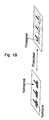
- Fig. 1A and Fig. 1B schematically show a preferred embodiment of the method for selectively coating a surface of a substrate.
- the wettability of surfaces by certain liquids is usually characterized by the contact angle of a liquid drop on the surface.
- Small contact angles mean that the liquid droplet spreads, so the wetting is very good.
- large contact angles mean that the liquid droplet stops, so that in the cross-sectional image very large angles arise between the substrate surface and the droplet surface, so the wettability is poor.
- this wettability effect is used to coat a surface with a liquid so that only the metal structures are wetted with the liquid.
- This effect of wettability can also be used to selectively coat a surface with liquid having at least a portion of plastic and at least a portion of inorganic material.
- FIG. 1A and Fig. 1B the basic features of this method are shown using the example of a polyimide film (PI film) with copper pads arranged on the surface of the PI film (Cu pads).
- PI film polyimide film
- Cu pads copper pads arranged on the surface of the PI film
- FIG. 1A the treatment of the structured metal surface with the polyimide film with the CF 4 / O 2 plasma, resulting in the different hydrophilic and hydrophobic areas and Fig. 1B shows the subsequent coating with liquid, whereby the liquid attaches in the hydrophilic areas (Cu pads), since they are much more wettable.
- the PI film becomes hydrophobic and the Cu pads hydrophilic. This results in the surface of the PI film areas of different surface energy, ie hydrophobic and hydrophilic areas, whereby a maximum difference in wetting behavior is achieved, which is then used for coating processes.
- plastic surfaces can be directly chemically modified by the direct action of a fluorine-containing plasma gas (CF 4 / O 2 plasma or CF 4 plasma).
- a fluorine-containing plasma gas CF 4 / O 2 plasma or CF 4 plasma.
- inorganic surfaces and also metals when exposed to a fluorine-containing plasma, primarily a cleaning effect due to a plasma etching process is observed. Accordingly, the action of the fluorine-containing plasma on the plastic surface results in hydrophobization of the surface, whereas metallic surfaces or inorganic surfaces are substantially only cleaned by the fluorine-containing gas, thereby maximizing the hydrophilicity of the metal surface or inorganic surface.
- the fluorine-containing plasma (CF 4 plasma or CF 4 / O 2 plasma) acts (fully) flat and directly on the entire plastic film.
- the organic surfaces of the plastic film are hydrophobicized, the inorganic or metallic surfaces are hydrophilized.
- a plastic substrate is provided as a substrate, on whose surfaces to be treated structured metal surfaces are present, wherein the plasma over the entire surface and acts directly on the entire surface, so that can be dispensed with a complex mask technique.
- the substrate can be rigid or flexible.
- the metal structures may be, for example, copper, aluminum or precious metals.
- the substrate may also consist of any material which is coated on one or both sides with a plastic layer, wherein on the surface of the plastic layer on one or both sides of the substrate metal structures are formed.
- the substrate is formed of any material which is coated with metal, wherein the metal in turn is coated by a plastic layer, and wherein said plastic layer has defined opening structures.
- the substrate may also be a metal foil which is coated on one or both sides with plastic, wherein this plastic layer in turn has defined opening structures.
- the production of the metal structures can either be done by a classical lithography process, as known from printed circuit board manufacture.
- the metal structures can be applied in structured fashion to the film or the plastic substrate by means of printing technology (inkjet or screen printing).
- the present method can be designed as a low-pressure plasma method, the plasma action can thus be carried out at a chamber pressure of 0.1 to 100 mbar.
- a chamber pressure of 0.1 to 100 mbar.
- use as atmospheric plasma is possible, which acts at normal pressure on the substrate surface.
- Suitable plasma gases are fluorine-containing gases, for example CF 4 , SF 3 , SF 6 or mixtures thereof with oxygen or nitrogen. Particularly advantageous has a mixture of 60 vol .-% CF 4 and 40 vol .-% O 2 or 80 vol .-% CF 4 and 20 vol .-% O 2 proved.
- liquid for the selective wetting water, solvents, varnishes, electrically insulating or conductive polymers and low-viscosity adhesives, etc. may be used.
- liquids containing solids or functional components can be applied, in which process variant the present process can be used as a sub-step for the self-assembly of small objects or components.
- the coating of the film substrate can be carried out in a continuous process.
- the substrate is brought into contact with a liquid. This can be done by dipping, knife coating, dispensing or printing.
- Another application is the selective and self-directed application of an adhesive layer on a surface. This can be used, for example, to place electrical or electronic components.
- wafer bonding with a structured adhesive layer. It is particularly advantageous here that even microstructured adhesive lines or adhesive surfaces can be coated automatically and selectively with adhesive. So it is not a complicated computerized dosing required.
- Another application is the coating of large-volume objects, especially with three-dimensionally shaped surfaces.
- Another application is the selective application of liquids containing solids or functional components.
- the present method can be used as a sub-step for the self-assembly of small objects or components.
- An advantage of the present method is that the plasma can act directly and preferably over the entire surface on the entire surface of the substrate.
- the use of a mask technique can be dispensed with to effect selective wetting of the structures.
- no photoresist layer is needed. This would be a disruptive layer as a structure of an electronic component, since it is not permanently stable.
- the present method is also applicable to plastic films. This allows the use of the new process for self-directed coating processes in the manufacture of electronic circuits on flexible substrates.
- the direct plasma effect can also be used for continuous processes (roll to roll).
Landscapes
- Engineering & Computer Science (AREA)
- Manufacturing & Machinery (AREA)
- Microelectronics & Electronic Packaging (AREA)
- Physics & Mathematics (AREA)
- Plasma & Fusion (AREA)
- Life Sciences & Earth Sciences (AREA)
- Wood Science & Technology (AREA)
- Application Of Or Painting With Fluid Materials (AREA)
- Manufacturing Of Printed Wiring (AREA)
Applications Claiming Priority (1)
| Application Number | Priority Date | Filing Date | Title |
|---|---|---|---|
| DE102007061465A DE102007061465A1 (de) | 2007-12-20 | 2007-12-20 | Verfahren zur selektiven Beschichtung einer Oberfläche mit Flüssigkeit |
Publications (1)
| Publication Number | Publication Date |
|---|---|
| EP2073615A1 true EP2073615A1 (fr) | 2009-06-24 |
Family
ID=40138034
Family Applications (1)
| Application Number | Title | Priority Date | Filing Date |
|---|---|---|---|
| EP08017970A Withdrawn EP2073615A1 (fr) | 2007-12-20 | 2008-10-14 | Procédé de revêtement sélectif d'une surface à l'aide de liquide |
Country Status (3)
| Country | Link |
|---|---|
| US (1) | US20090162566A1 (fr) |
| EP (1) | EP2073615A1 (fr) |
| DE (1) | DE102007061465A1 (fr) |
Families Citing this family (5)
| Publication number | Priority date | Publication date | Assignee | Title |
|---|---|---|---|---|
| DE102009050426B3 (de) * | 2009-10-22 | 2011-03-31 | Fraunhofer-Gesellschaft zur Förderung der angewandten Forschung e.V. | Verfahren zum ausgerichteten Aufbringen von Bauteilen auf einem Trägersubstrat und ein Verfahren zur Herstellung eines Trägersubstrats dafür und ein Verfahren zur Bestückung eines Zielsubstrats damit. |
| DE102010045035A1 (de) * | 2010-09-10 | 2012-03-15 | Siemens Aktiengesellschaft | Verkapselung und Herstellen einer verkapselten bestückten Leiterplatte |
| US20150004750A1 (en) * | 2013-06-27 | 2015-01-01 | Stats Chippac, Ltd. | Methods of Forming Conductive Materials on Contact Pads |
| DE102014224276B4 (de) * | 2014-11-27 | 2021-12-30 | Fraunhofer-Gesellschaft zur Förderung der angewandten Forschung e.V. | Verfahren zum hochpräzisen Drucken von Strukturen auf Oberflächen sowie Substrat mit einer eine gedruckte Struktur aufweisenden Oberfläche |
| US10120411B2 (en) * | 2016-08-22 | 2018-11-06 | Apple Inc. | Systems with low-friction matte flexible printed circuits |
Citations (5)
| Publication number | Priority date | Publication date | Assignee | Title |
|---|---|---|---|---|
| US4946549A (en) * | 1989-10-27 | 1990-08-07 | At&T Bell Laboratories | Method for fabricating or modifying an article comprising the removal of a polymer coating |
| DE3936955C1 (en) * | 1989-11-06 | 1991-01-24 | Wls Karl-Heinz Grasmann Weichloetanlagen- Und Service, 6981 Faulbach, De | Plasma treating conductor plates for electronic elements - with process gas e.g. oxygen, hydrogen, fluoro-(chloro)-hydrocarbon, etc. before soldering |
| US6046500A (en) * | 1996-10-31 | 2000-04-04 | International Business Machines Corporation | Method of controlling the spread of an adhesive on a circuitized organic substrate |
| US20050003645A1 (en) * | 2003-05-27 | 2005-01-06 | Seiko Epson Corporation | Forming process of thin film pattern and manufacturing process of device, electro-optical apparatus and electronic apparatus |
| GB2430547A (en) * | 2005-09-20 | 2007-03-28 | Seiko Epson Corp | A method of producing a substrate having areas of different hydrophilicity and/or oleophilicity on the same surface |
-
2007
- 2007-12-20 DE DE102007061465A patent/DE102007061465A1/de not_active Ceased
-
2008
- 2008-10-14 EP EP08017970A patent/EP2073615A1/fr not_active Withdrawn
- 2008-12-18 US US12/338,198 patent/US20090162566A1/en not_active Abandoned
Patent Citations (5)
| Publication number | Priority date | Publication date | Assignee | Title |
|---|---|---|---|---|
| US4946549A (en) * | 1989-10-27 | 1990-08-07 | At&T Bell Laboratories | Method for fabricating or modifying an article comprising the removal of a polymer coating |
| DE3936955C1 (en) * | 1989-11-06 | 1991-01-24 | Wls Karl-Heinz Grasmann Weichloetanlagen- Und Service, 6981 Faulbach, De | Plasma treating conductor plates for electronic elements - with process gas e.g. oxygen, hydrogen, fluoro-(chloro)-hydrocarbon, etc. before soldering |
| US6046500A (en) * | 1996-10-31 | 2000-04-04 | International Business Machines Corporation | Method of controlling the spread of an adhesive on a circuitized organic substrate |
| US20050003645A1 (en) * | 2003-05-27 | 2005-01-06 | Seiko Epson Corporation | Forming process of thin film pattern and manufacturing process of device, electro-optical apparatus and electronic apparatus |
| GB2430547A (en) * | 2005-09-20 | 2007-03-28 | Seiko Epson Corp | A method of producing a substrate having areas of different hydrophilicity and/or oleophilicity on the same surface |
Non-Patent Citations (3)
| Title |
|---|
| J. SEO ET AL.: "Self-Assembly Templates by Selective Plasma Surface Modification of Micropatterned Photoresist", IEEE, 2002 |
| N.A. BULLETT ET AL.: "Polymer surface micropatterning by plasma and VUVphotochemical modification for controlled cell culture", APPLIED SURFACE SCIENCE, vol. 235, 2004, pages 395 - 405 |
| U. SRINIVASAN; D. LIEPMANN; R.T. HOWE: "Microstructure to Substrate Self-Assembly Using Capillary Forces", JOURNAL OF MICROELEKTROMECHANICAL SYSTEMS, vol. 10, 2001, pages 17 - 24, XP001123703, DOI: doi:10.1109/84.911087 |
Also Published As
| Publication number | Publication date |
|---|---|
| DE102007061465A1 (de) | 2009-06-25 |
| US20090162566A1 (en) | 2009-06-25 |
Similar Documents
| Publication | Publication Date | Title |
|---|---|---|
| DE69935179T2 (de) | Strukturierungstechnik unter Verwendung eines Templates und Tintenstrahlsystems | |
| EP2247766B1 (fr) | Procédé pour produire des surfaces structurées | |
| DE10240105B4 (de) | Herstellung organischer elektronischer Schaltkreise durch Kontaktdrucktechniken | |
| DE2741417B2 (de) | Verfahren zur Herstellung einer Grundplatte für eine gedruckte Schaltung | |
| EP3326437B1 (fr) | Procédé de production de revêtements structurés sur une pièce moulée et dispositif permettant la mise en oeuvre dudit procédé | |
| EP2073615A1 (fr) | Procédé de revêtement sélectif d'une surface à l'aide de liquide | |
| EP3592501B1 (fr) | Procédé servant à fabriquer un masque technique | |
| EP1395633B1 (fr) | Procede de production de couches minces homogenes par serigraphie | |
| DE102011076994A1 (de) | Tintenstrahldruckknopf mit Selbstreinigunsvermögen zum Tintenstrahldrucken | |
| DE102009050426B3 (de) | Verfahren zum ausgerichteten Aufbringen von Bauteilen auf einem Trägersubstrat und ein Verfahren zur Herstellung eines Trägersubstrats dafür und ein Verfahren zur Bestückung eines Zielsubstrats damit. | |
| DE102016200046A1 (de) | Lötmaskenzusammensetzungen für Aerosol-Jet-Druck | |
| KR20150108893A (ko) | 다중 성분 표면상에서 표면 기처리 및 방울 확산 제어 | |
| DE102013109879A1 (de) | Fügeverfahren, Material- oder Phasentransformationsverfahren, Sicherungsverfahren, Fügemittel und Sicherheitssystem unter Verwendung reaktiver Materialsysteme | |
| DE102005063510B4 (de) | Verwendung eines Verfahrens zur Beschichtung einer Druckschablone eines SMT-Prozesses | |
| DE102011083733A1 (de) | Siebdruckschablone und Verfahren zum Beschichten von Siebdruckschablonen | |
| DE10254927B4 (de) | Verfahren zur Herstellung von leitfähigen Strukturen auf einem Träger und Verwendung des Verfahrens | |
| WO2015063080A1 (fr) | Dispositif et procédé permettant de traiter des surfaces métalliques au moyen d'un liquide de gravure | |
| DE102005018984A1 (de) | Verfahren und Vorrichtung zum Herstellen von elektronischen Bauteilen | |
| EP1879435A2 (fr) | Structures électriques conductrices | |
| DE102009006064B4 (de) | Verfahren zur Herstellung eines mikrostrukturierten Films | |
| DE102008045540B4 (de) | Verfahren zur Herstellung eines mikrostrukturierten Films | |
| EP4010200B1 (fr) | Procédé de masquage de surfaces à mater | |
| WO1999053738A1 (fr) | Procede et dispositif pour realiser des structures a couches minces | |
| EP2200930B1 (fr) | Procédé d'impression d'une nanostructure et/ou d'une microstructure | |
| DE19817530A1 (de) | Verfahren und Vorrichtung zur Herstellung von Dünnschichtstrukturen |
Legal Events
| Date | Code | Title | Description |
|---|---|---|---|
| PUAI | Public reference made under article 153(3) epc to a published international application that has entered the european phase |
Free format text: ORIGINAL CODE: 0009012 |
|
| AK | Designated contracting states |
Kind code of ref document: A1 Designated state(s): AT BE BG CH CY CZ DE DK EE ES FI FR GB GR HR HU IE IS IT LI LT LU LV MC MT NL NO PL PT RO SE SI SK TR |
|
| AX | Request for extension of the european patent |
Extension state: AL BA MK RS |
|
| AKX | Designation fees paid | ||
| STAA | Information on the status of an ep patent application or granted ep patent |
Free format text: STATUS: THE APPLICATION IS DEEMED TO BE WITHDRAWN |
|
| 18D | Application deemed to be withdrawn |
Effective date: 20091228 |
|
| REG | Reference to a national code |
Ref country code: DE Ref legal event code: 8566 |